Your browser does not fully support modern features. Please upgrade for a smoother experience.
Please note this is an old version of this entry, which may differ significantly from the current revision.
Subjects:
Engineering, Environmental
The End-of-Life (EoL) management of photovoltaic (PV) modules has always present significant concern to the scientific community, especially when large scale emergence of PV waste is expected in the near future. As PV waste contains rare and hazardous materials as its composition, its unregulated disposal poses the problem of polluting the environment and wastage of potentially usable resources. Hence, researchers have delved into the recycling and recovery of materials from PV waste to improve the sustainability of the EoL management of PV modules.
- end-of-life (EoL) PV modules
- PV waste management
- PV recycling
- high-value recycling
1. PV Modules
The components of a PV system can be divided into 2 main categories: PV modules and balance of system (BOS), the latter of which are the remaining components that support and complement the PV system [23,24]. Generally, the modules are divided into three groups, which are the wafer-based silicon modules, thin-film modules and emerging technologies [23,26]. The wafer-based silicon technologies, also known as first generation technologies, include monocrystalline (mono-Si), multi- or polycrystalline (poly-Si) and ribbon silicon modules. The second generation thin-film modules include cadmium telluride (CdTe), copper indium gallium (di)selenide (CIGS) and amorphous silicon (a-Si) modules. Some examples of third generation emerging technologies are organic PV (OPV), dye-sensitised cells, copper zinc tin sulphide (CZTS), perovskite and concentrating PV technologies (CPV) [4,26].
In terms of market share, c-Si PV modules have always dominated with a percentage share of between 80% to 90% [1,27], with thin-film modules technologies following behind at around 7% to 10%. Meanwhile, the market share of emerging technologies is still minimal (~1%) [4]. Hence, this review focuses on discussing first and second generation technologies, as there is limited information on the recycling of emerging technologies [28,29].
2. Disposal of PV Materials
Currently, the treatment methods of EoL PV modules include disposal, incineration and recycling. Repairing and refurbishing are also viable methods for treating EoL modules, but they are still in the earlier stages of research compared to recycling [8,47].
Globally, EoL PV materials are mostly disposed of in landfills or incinerated [1,21]. This is due to the limited waste stream of EoL PV modules currently present in most countries, which does not spark significant concern or financial justification to establish a sustainable PV materials recycling system in the country [48]. Depending on the country’s policies, PV modules can be classified as either hazardous waste (HW) or non-hazardous waste (non-HW) [4,49].
Although the disposal of PV modules may be regulated, there are several negative environmental impacts that heavily discourage the landfill disposal of EoL PV modules. One of the main issues is the leaching of hazardous substances from the PV modules. The hazardous compounds present in the modules, such as lead (Pb) and silver (Ag) from c-Si PV modules and cadmium (Cd) and selenium (Se) from thin-film modules, can induce both acute toxicity in humans and animals, as well as external environmental costs of air, water and soil pollution [21,50]. A life cycle analysis (LCA) study has shown that the environmental impacts of disposing of poly-Si modules were always greater than recycling [37]. Similarly, another study has also discovered that the landfill disposal of silicon and wafer waste from the manufacturing of PV modules contributed up to 95% of the human toxicity potential (HTP) [51].
Secondly, landfill disposal of PV materials also leads to loss of potentially reusable resources such as glass, aluminium (Al) and other rare metals (Ag, indium (In), gallium (Ga), and Se). These resources are essentially wasted as they are not recoverable from landfills, and thus economic loss would be incurred [18,52]. An LCA study has shown that among the environmental impacts caused by landfilling c-Si PV modules, the greatest impact was present in the metal depletion category as valuable materials are lost [53]. The primary production of copper (Cu), Ag, Al and Si are highly energy-intensive and environmentally burdensome, thus when these materials are lost, the same energy-intensive production has to be employed again to produce the same amount of materials [53].
As evidenced from the negative environmental impacts, landfill disposal is not a preferred option to manage EoL PV modules. There are still potential consequences that need to be addressed even though PV modules have been disposed of responsibly.
3. Recycling of PV Materials
The recycling of PV materials can be differentiated into open-loop recycling and closed-loop recycling [1]. Open-loop recycling is where the materials are recovered in lower quality, while closed-loop recycling emphasises recovering secondary materials that are of equal quality to the original PV materials. In comparison, it is more preferable to carry out closed-loop recycling, as high-quality secondary materials can be directly fed into the supply chain to remanufacture into new PV modules [1,54]. Closed-loop recycling is also heavily associated with high-value recycling, where instead of only bulk components such as glass, Al and Cu are recycled (bulk recycling), semiconductors and rare metals are recovered, with a focus on higher recovery rates as well [19]. The combination of these two is essential in shaping a circular economy within the PV industry, as almost every material within an EoL PV module can be reclaimed and reused, thereby minimising the depletion of resources [8,55]. As a consequence, there would be significant reduction of valuable materials being sent to landfill, and materials can be conserved for large-scale application of PV in the near future [45].
Unfortunately, the current situation in most countries is that only those high value materials present in sufficient concentrations to be economically extracted are recycled [43]. Therefore, the bulk recycling of PV modules is still the current industrial norm, whereby the modules are recycled within existing general recycling plants to reclaim the major components [4,11]. This approach is most common as it is relatively low-cost, but it is not sustainable in the long term when the environmental impacts of re-processing the raw materials are taken into consideration [1].
The recycling processes of c-Si modules and thin-film CdTe modules are different due to the differences in their module structure and metal composition. However, they are similar in terms of the necessities required to eliminate the encapsulant and to recover the materials contained within the modules (Figure 1). In both types of modules, the degree of glass–EVA (ethylene vinyl-acetate) separation heavily determines the value of the recovered glass [11], and the polymeric material needs to be completely removed in order for the glass to be used as cullets in soda-lime glass manufacturing of flat glass [56].
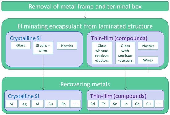
Figure 1. Separation process for recycling of PV modules [57].
3.1. Recycling of c-Si Modules
Currently, c-Si modules are mainly treated in bulk recycling plants designed for treating laminated glass, electronic waste and metals. In these facilities, a mechanical approach of crushing and sorting is employed to recover only bulk materials such as glass, Al frames and Cu [11,25]. Meanwhile, the remaining silicon cells and other materials including plastics are incinerated or disposed. According to IRENA [4], the cumulative recovery yields of these bulk materials can achieve more than 85% by panel mass just through mechanical separation. However, the treatment capacity of these facilities is low and the glass recovered is recycled as low-grade product [57]. Thus, in order to accomplish high-value recycling with greater recovery yields, further treatment of thermal, chemical or metallurgical methods are needed to recover the semiconductor materials [4].
The first step of recycling c-Si PV modules is to separate the major components, which are the Al frames, junction boxes, wiring and laminated glass [22,35]. This can be done through manual separation, thermal treatment or automatic separation [25,35,58]. Next, the EVA encapsulant layer sealing the silicon cells has to be removed through thermal, chemical or mechanical treatment. These studies have shown that thermal treatment of the EVA layer is more preferable compared to chemical treatment which requires usage of expensive and toxic reagents [35,59]. Besides, the effectiveness chemically treating the EVA layer is quite low, as the time duration needed to delaminate the glass is too long. Additionally, thermal treatment is usually able to recover glass and the silicon cells without breakage compared to most of the mechanical processes [19,57]. The heating condition or requirement of a pretreatment during thermal treatment is fairly important so as to avoid damaging the silicon cells, which can fetch a higher price in an unbroken state [50,60].
After removing the EVA layer, the next step is to recover the silicon wafer from the silicon cells. Conventionally, this process is carried out via chemical etching, which utilises acidic or basic solutions to sequentially remove the metal electrodes, anti-reflective coating (ARC) and n-p junction on the surface of the silicon cells [35,61]. However, there also exists laser treatment for removing the coating on the silicon cells, as demonstrated by this study [59]; however, the cost of employing this method is high and its effectiveness is low compared to chemical etching. In addition, a study [62] proposed a combination of chemical and mechanical treatment to remove the silicon cell coatings in an effort to reduce the use of hazardous chemicals such as hydrogen fluoride (HF), nitric acid (HNO3) and phosphoric acid (H3PO4).
The processes discussed above are general treatment methods for a complete recycling of c-Si PV modules. As summarised in Table 1, there are variations in the methods used depending on the studies and corporations.
Table 1. Recycling processes of c-Si and CdTe modules from different literature and corporations. The symbol ‘✓’ represents the presence of the type of treatment process.
| PV Module | Recycling Processes | Yield of Materials | Suitable for Broken Modules | References | ||||||
|---|---|---|---|---|---|---|---|---|---|---|
| Disassembly and Delamination | Recovery of Materials | |||||||||
| Mechanical Treatment | Thermal Treatment |
Chemical Treatment |
Optical Treatment | Mechanical Treatment | Chemical Treatment | Laser Treatment | ||||
| c-Si | ✓ | ✓ | Silicon powder/sheets | Yes | [35] | |||||
| c-Si | ✓ | ✓ | ✓ | ✓ | Pure silicon cells | Yes | [59] | |||
| c-Si | ✓ | ✓ | ✓ | Ag Al Silicon wafers |
Not specified | [62] | ||||
| c-Si | ✓ | ✓ | Al: 94% Glass Si: 80% Cu: 79% Ag: 90% Pb: 93% |
Not specified but chemical etching is applicable to broken cells | [50] | |||||
| c-Si, a-Si and CdTe | ✓ | ✓ | Glass: 80–85% | Not specified but broken modules can be treated together during crushing | [56] | |||||
| c-Si (LGRF) | ✓ | ✓ | Glass: 92% Cu: 41% Al: 74% |
Not specified but broken modules can be treated together during crushing | [25,53] | |||||
| c-Si (FRELP) | ✓ | ✓ | ✓ | ✓ | Glass: 99% Cu: 69% Al: 99% Si: 95% Ag: 95% |
Not specified | [53,58] | |||
| c-Si (Deutsche Solar AG) | ✓ | ✓ | Glass Al Cu Si Wafers |
Yes | [63] | |||||
| c-Si (YingLi Solar) | ✓ | ✓ | Glass Al EVA Si Ag Tedlar |
Not specified but broken modules can be treated together during smashing | [8,64] | |||||
| c-Si (Veolia) | ✓ | ✓ | Glass Al Plastic Si Metals |
Not specified | [8,65] | |||||
| c-Si (NPC Group) | ✓ | ✓ | Glass Al EVA Solar cells |
Not specified | [8,66] | |||||
| CdTe (Solar Cells Inc., currently First Solar) | ✓ | ✓ | ✓ | ✓ | Glass Te sludge: 80% Back metals: 93% Cd: 85% |
Yes for chemical treatment but not suitable for water blasting | [67] | |||
| CdTe (First Solar) | ✓ | ✓ | Glass: 90% Cu Unrefined CdTe semiconductor: 95% |
Yes | [25,68,69] | |||||
| CdTe and CdS (ANTEC Solar) | ✓ | ✓ | ✓ | Glass CdCl2 TeCl4 |
Not specified but broken modules can be treated together during milling | [8,44] | ||||
| CdTe and CIS (RESOLVED) | ✓ | ✓ | ✓ | ✓ | Glass Cd Te In |
Yes | [45] | |||
| CdTe and CIGS (Loser Chemie) |
✓ | ✓ | Al Glass with EVA layer Glass Metals |
Yes | [57] | |||||
The recycling processes provided by Granata et al. [56], the laminated glass recycling facility (LGRF) [25,53], YingLi Solar [64] and NPC group [66] are considered to be bulk recycling as semiconductor materials and precious metals are not recovered. On the other hand, the studies by Jung et al. [50], Park et al. [62] and the industrial pilot-scale project (Full-Recovery End of Life Photovoltaics (FRELP)) [58] are examples of high-value recycling where both bulk materials and semiconductor materials are reclaimed. The other treatment processes [35,59,65] are considered as semi-high-value recycling, as some of them recover only silicon wafer but no other precious metals. Meanwhile, the Deutsche Solar AG recycling process is closed-loop recycling which integrates reclaimed cells back into a standard PV module production line [34,63].
With the environmental impacts from the production of virgin silicon cells in mind, it is highly recommended to employ high-value and closed-loop recycling processes to recover silicon wafer, especially in an unbroken state [57,61]. This is because even if the cells have damage such as microcracks or edge chipping, they cannot be recycled into a whole wafer and have to be crushed into powder form to be used for silicon ingot production again [57,62]. Besides, high-value recycling processes have lower environmental impacts due to the displacement of primary production from the increased yields and greater profits from the higher quality of the materials recovered [53,70].
Although most of the recycling processes are carried out on intact c-Si PV modules, some processes, such as those from Klugmann-Radziemska and Ostrowski [35] as well as Deutsche Solar, are applicable for broken or damaged PV modules. After the removal of external major components and initial thermal delamination treatment, the modules are usually crushed for further treatment; thus, broken modules can still be recycled [67] but the broken wafers cannot be remade into new wafers.
3.2. Recycling of CdTe Thin-Film Modules
In a study by IEA [57], most patents on thin-film modules recycling indicated a focus on high-value recycling and the patent assignees for thin-film modules recycling were mostly corporations (95% of patents for thin-film modules recycling), suggesting that thin-film modules recycling patents are more likely to be commercialised [57]. Furthermore, in thin-film modules recycling, the recovery of semiconductor materials, despite being in very small quantities, is more important than the recovery of glass due to the scarcity of semiconductor materials [30]. Hence, CdTe thin-film modules are more commonly recycled in dedicated recycling plants instead of being bulk recycled in existing recycling plants [25].
Similar to c-Si PV modules, the first step of recycling CdTe thin-film modules is to remove the junction box. Next, the encapsulant sealing the semiconductors between the cover glass and glass substrate has to be removed, mainly through mechanical or thermal means. However, there is a study by Palitzsch (as cited by [57]) that used an optical approach to separate the glass layers in thin-film modules. Then, the semiconductor materials on the glass substrate are stripped off, usually by chemical etching; however, the mechanical method of stripping semiconductors off the glass is also being investigated [45,67]. The various recycling processes for CdTe thin-film modules are presented in Table 1.
These studies [67,68,69,71] presented the recycling processes of CdTe modules by First Solar, a commercial CdTe thin-film module manufacturer. These studies have displayed the evolution of First Solar recycling processes, although a high-value recycling principle has been applied since the first study. Through First Solar’s recycling processes, approximately 90% of the weight of a CdTe module can be recovered, consisting mainly of glass which can be reused in new glass product [68].
ANTEC Solar has developed a patented process for recycling CdTe and CdS thin-film PV modules by treating the modules in a gaseous environment [44]; this proves is distinct from the other chemical etching processes where wet chemicals are used. Meanwhile, Berger et al. [45] have examined the feasibility of the wet-mechanical process in recovering metals from thin-film modules. The advantage of the wet-mechanical process is its lack of chemical usage; however, there are considerable losses of valuables, resulting in low efficiency compared to conventional chemical etching [45].
For thin-film modules, as there are no materials requiring to be intact during recycling (as in Si cell), the mechanical approach to delaminating thin-films modules is not discouraged. Furthermore, crushing the modules into smaller particles enhances the performance of the subsequent chemical etching process [57], hence even broken modules can be treated in the same processes. Aside from that, most processes are not just applicable to CdTe and can be suitable for other thin-film modules as well. For instance, First Solar recycling process is applicable to CIS thin-film modules, albeit with the recovery chemistry for indium requiring further investigation [71].
3.3. Benefits of Recycling
Recycling EoL PV modules provides numerous benefits, especially to the environment. The environmental performance of recycling can be analysed via the approach of LCA, which has been carried out by many studies, as summarised in [22]. The main benefit of recycling PV modules is the reduction of the energy use and emissions associated with raw material production and the usage of secondary materials. In contrast to its zero emissions operational stage, the EoL recycling stage of PV modules consumes energy and release emissions due to the usage of fossil fuel in the recycling processes. However, a few studies have shown that the environmental impacts from recycling are very little compared to those of the production of the PV modules [25,36,69,70,72]. In addition, the recovery of materials from recycling to produce secondary resources offsets the energy use and emissions related to virgin material production, as shown by several LCA studies studies [16,25,41,53,63,69,73,74,75]. A recent LCA study has demonstrated that the environmental impacts of producing c-Si cells from recycled materials were 58% lower than production of cells from virgin materials. The results were mainly due to decreased energy consumption from processing raw silicon [61]. Furthermore, a study has shown that the supply of semiconductor materials, including In, Ga, Se and tellurium (Te), will have their reserves depleted in 5 to 50 years at the current rate of extraction [76]. Therefore, there are greater motivations to recycle PV modules, including the recovery of the valuable materials contained within them to prevent the deficit of raw materials [20,29] and the reduction of the environmental impacts caused by the processing of raw materials.
Compared to a landfill disposal scenario, the recycling of PV modules is able to reduce the amount of waste and waste-related emissions [4,77]. According to Vellini et al. [37], the recycling of poly-Si modules was able to reduce the terrestrial eco-toxicity potential (TETP) by 73.58%, fresh water aquatic eco-toxicity potential (FAETP) by 67.4% and acidification potential (AP) by 37.48% compared to EoL without recycling scenario. Furthermore, environmental credits are given when energy recovery is established during thermal treatment or incineration of PV modules, leading to significant reduction in terms of ozone layer depletion potential (OLDP) (27%), ionising radiation human health (25%) and freshwater eutrophication (18%), as evidence by this LCA study [58].
In addition to environmental benefits, recycling PV modules also brings about economical profitability. IRENA has estimated that the material value of material that can be recovered from recycling PV modules by 2030 and 2050 amounts to USD 450 million and 15 billion, respectively [4]. These impressive economic values are obtained from the secondary materials embodied within the EoL PV modules, which are locked away when PV modules are manufactured and cannot be accessed until the lifetime of a PV module is over [78]. Recycling PV modules recovers these materials, and reselling them into the global market helps stimulate a market for secondary raw materials [4]. Besides this, these secondary materials can help keep the costs of PV materials low due to their lower pricing [77]. Furthermore, the establishment of new PV EoL industries can yield new employment opportunities such as waste collectors, pre-treatment companies, producers and installation companies [4,23], hence providing economic growth to the country.
Additionally, setting up proper recycling infrastructure for PV modules further reinforces the ‘clean’ image of the solar PV system. Proper recycling can answer public concerns about the toxicity of hazardous materials present in PV modules by demonstrating that those materials can be recovered instead of being disposed in an unregulated way [71,79]. This can assist the large-scale penetration of PV in the market [72] due to the assurance offered by the proper management of EoL PV modules.
This entry is adapted from the peer-reviewed paper 10.3390/su14148567
This entry is offline, you can click here to edit this entry!