Your browser does not fully support modern features. Please upgrade for a smoother experience.
Please note this is an old version of this entry, which may differ significantly from the current revision.
A photovoltaic (PV) cell is the essential unit of a solar energy generation system in which sunlight is promptly converted to electrical energy. The solar cell is a p-n junction device. n-type refers to the negatively charged electrons donated by donor impurity atoms and p-type refers to the positively charged holes created by acceptor impurity atoms
- photovoltaic (PV)
- semiconductors
- gallium arsenide (GaAs)
1. Introduction
Global environmental concerns and the increasing energy demand, coupled with continuous progress in renewable energy technology, are encouraging the utilization of alternative energy resources. Solar energy is the most affordable and abundant of all long-term natural resources to date [1]. Solar PV technology is one of the optimum ways to utilize solar power to generate electricity by converting the sunlight to direct current in solar cells or PV cells [2][3].
PV energy conversion utilizes devices based on electronic semiconductors, particularly but not exclusively, crystalline silicon (c-Si) or thin-film semiconductor materials. A (c-Si) based solar system is usually constructed from two essential types of crystalline materials, monocrystalline and multi-crystalline solar modules. Single-crystal semiconductors have superior electrical characteristics (20% efficiency) comparable to polycrystalline materials. Nevertheless, monocrystalline PV modules are non-economical as crystalline wafer-based technology is too expensive [4][5].
Thin film technology is an alternative technique that uses usually amorphous silicon (a-Si) or other semiconductor materials (i.e., cadmium telluride (CdTe), copper indium gallium selenide (CIGS), or gallium arsenide (GaAs)) in its structure. A thin-film solar cell is much thinner than a conventional (c-Si) cell. The film’s thickness is a few nanometers (nm) to tens of micrometres (μm), which allows thin-film modules to be light and flexible. Furthermore, thin-film technology is generally cost-effective as compared to (c-Si) wafer-based technology [6][7].
The (a-Si) solar cell is one of the most common thin-film technologies with cell efficiency (5–7%). The efficiency increases with double and triple junction design to 8–10%. (a-Si) thin-film offers lower efficiency when compared to the (c-Si) module. In addition, (a-Si) thin film is prone to degradation due to the reaction of (a-Si) with the environment, such as with the air or water vapour [8][9].
Furthermore, CdTe thin film nearly competes with the (c-Si) cell in cost/watt. Nevertheless, tellurium supplies are restricted and cadmium is highly poisonous [10].
Moreover, CIGS PV cell is another film technology with an acceptable cell efficiency of (~20%). However, the cost of fabrication CIGS solar cell is higher than CdTe- based thin film and (c-Si) wafer [11].
Moreover, GaAs thin film is a crystalline compound form of (Ga) and (As). It has a high resistivity to heat and radiation, which affect the efficiency of solar cells. Although a GaAs solar module is expensive, it holds the world’s record in efficiency (over 30%). Since the industry favours efficiency over cost for outer space power generation, multijunction GaAs cells are usually used for concentrator solar structures and spacecraft-based solar energy as they can be operated at an extremely higher temperatures compared to a (c-Si) based solar system [12][13][14].
 Figure 1. A p-n junction PV cell.
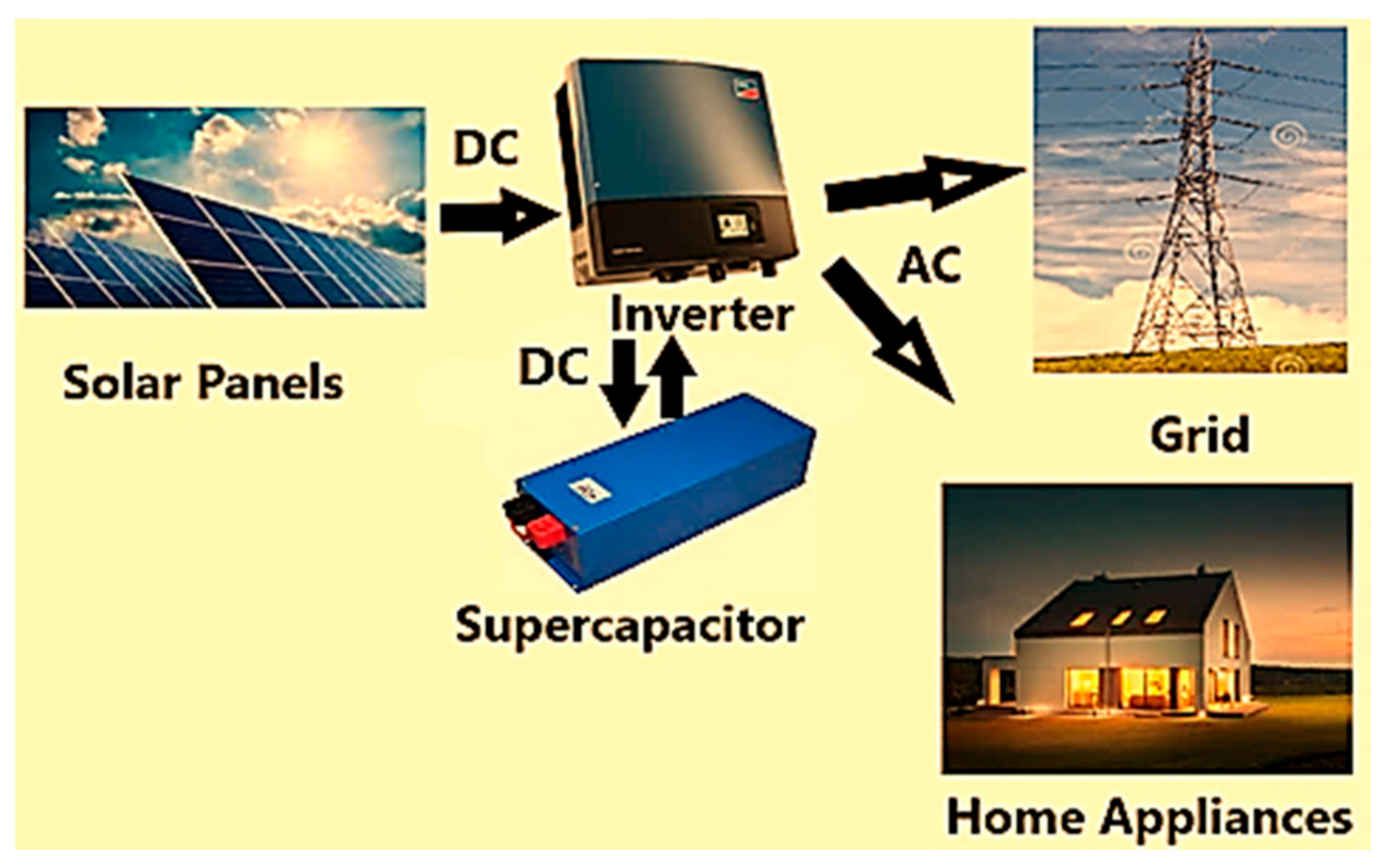 Figure 2. The basic components of a PV system.
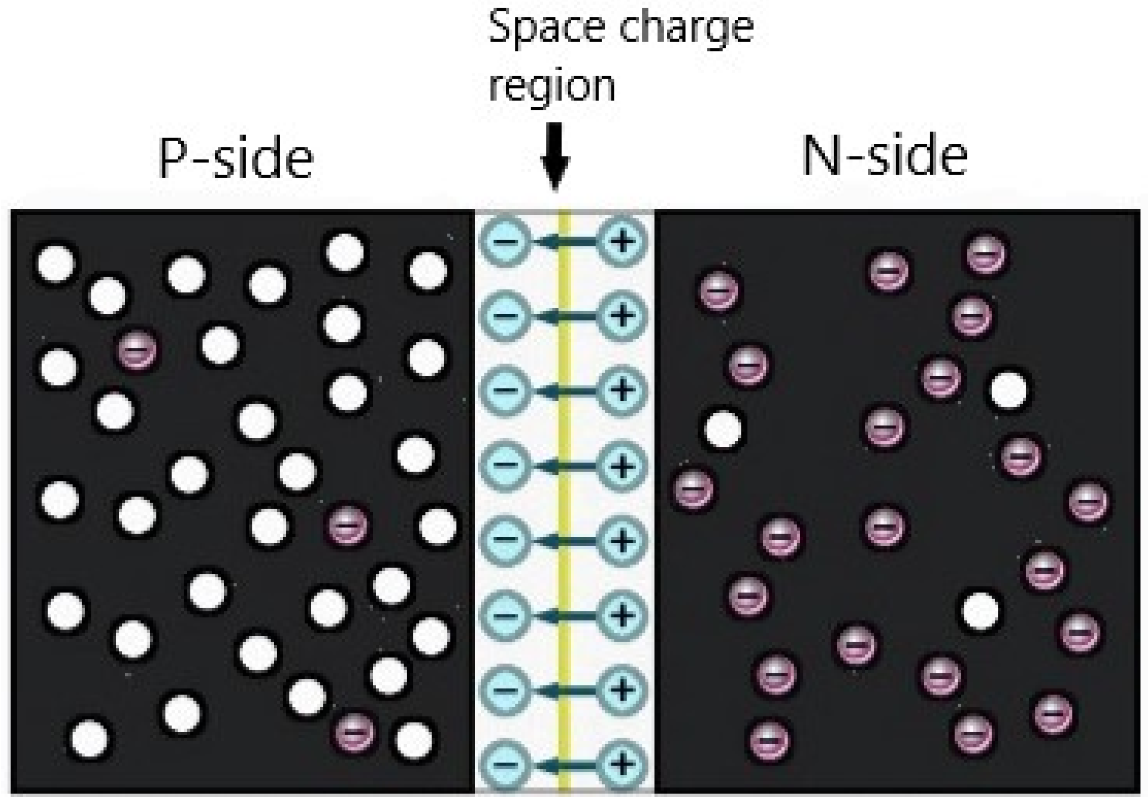 Figure 3. The basic semiconductor form at the instant connection of the p-n sections and generating the electric field in the space charge region.
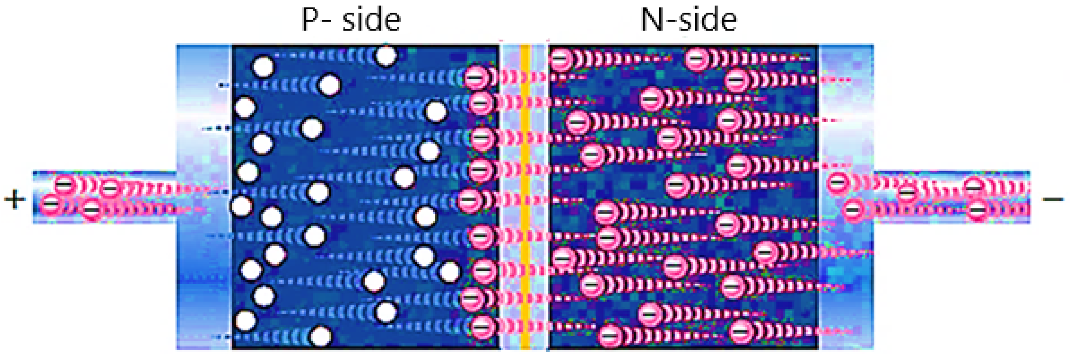 Figure 4. The flow of majority carriers in a forward-biased diode.
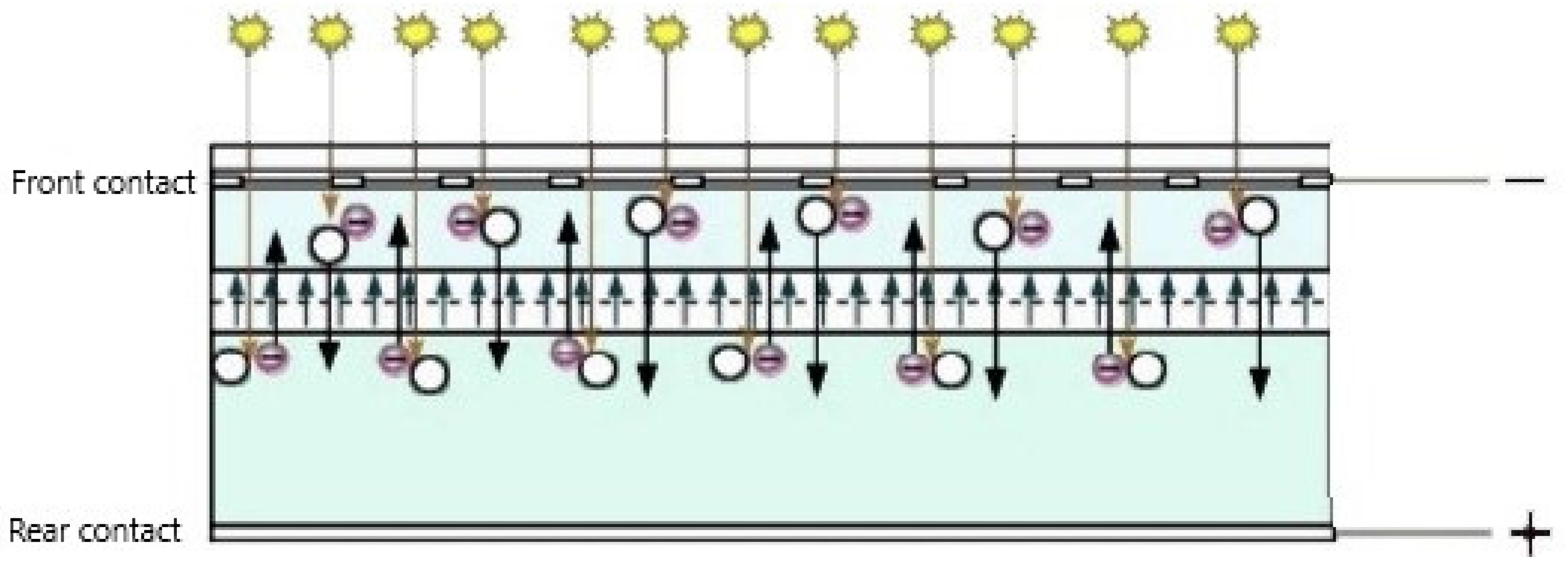 Figure 5. The PV cell under illumination.
 Figure 6. The practical equivalent circuit of a solar cell.
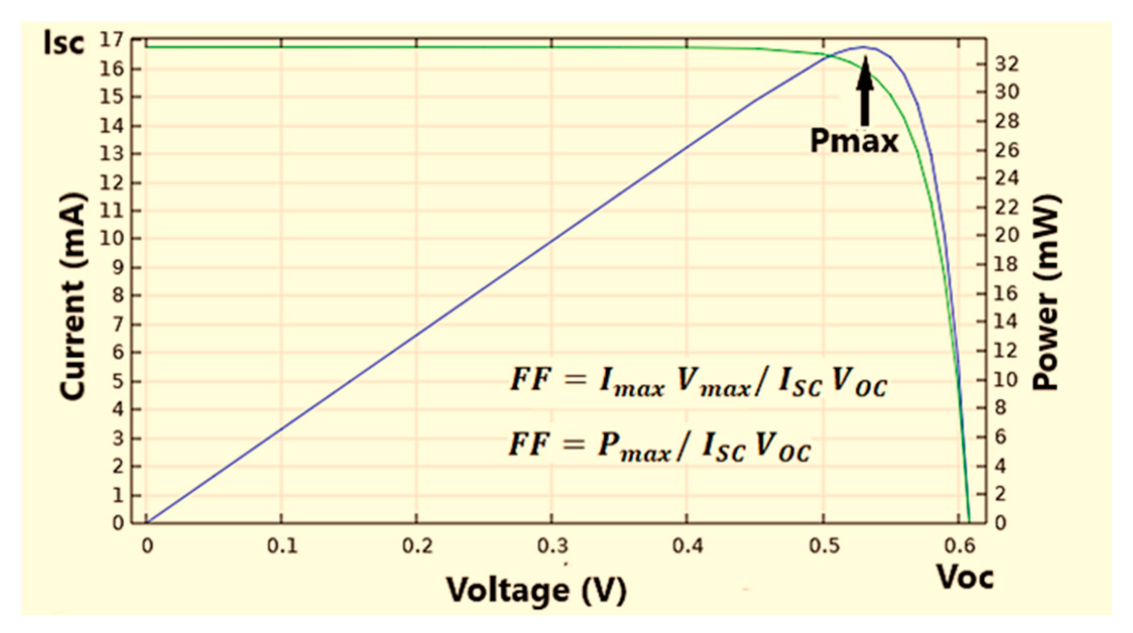 Figure 7. (I-V) and (P-V) characteristics of a solar cell under illumination.
2. Solar Cells
2.1. The Working Principle of PV Cells
A PV cell is the essential unit of a solar energy generation system in which sunlight is promptly converted to electrical energy. The solar cell is a p-n junction device. n-type refers to the negatively charged electrons donated by donor impurity atoms and p-type refers to the positively charged holes created by acceptor impurity atoms, referring to Figure 1 of a PV structure [15][16][17].
Figure 1. A p-n junction PV cell.The working principle of solar cells is based on the photovoltaic effect. The PV effect can be divided into three essential procedures [18][19][20].
-
Absorption of photons in a p-n junction electronic semiconductor to generate the charge carriers (electron-hole pairs). The absorption of a photon with energy (E = hυ) higher than the gap energy ‘Eg’ of the doped semiconductor material means that its energy is used to excite an electron from the valence band ‘Eυ’ to the conduction band ‘Ec’ leaving a void (hole) at the valance level. Additional kinetic energy is given to the electron or hole by the excess photon energy (hυ–hυ0). ‘hυ0′ is the minimum energy or work function of the semiconductor required to generate an electron-hole pair. The work function here represents the energy gap. The excess energy is dissipated as heat in the semiconductor [21][22].
-
Consequent separation of the light-generated charge carriers. In an external solar circuit, the holes can flow away from the junction through the p-region, and electrons can flow out across the n-region and pass through the circuit before they recombine with the holes.
-
Finally, the separated electrons can be used to drive an electric circuit. After the electrons passed through the circuit, they will recombine with the holes.
The n-type must be designed thinner than the p-type. Thus, the electrons can pass through the circuit in a short time and generate current before they recombine with the holes. Besides, an anti-reflective coating is applied over the n-layer to reduce surface reflection and enhance the transmission of the light to the semiconductor material.
All the aspects presented in this section will be discussed in more detail in the next sections.
2.2. Solar Cell Panels
Solar panels are multiple solar cells connected in series and parallel to produce a certain power output. One PV cell is unfeasible for most applications as it can only produce about 0.5 V. For example, six cells are connected in series, the cell is assumed to have the same current as a single cell and ideal 3 V (6 × 0.5 V). Series cells are also connected in parallel for higher current capacity. If the six cells can generate 2 A, the series-parallel structure of twelve cells is supposed to generate 4 A and 3 V [23].
2.3. Components of Solar Power System
A PV system is composed of a solar panel, supercapacitor, and inverter. The solar panel absorbs photon energy and transforms it into electricity through the PV mechanism. The supercapacitor backup is used to deliver additional energy only on sunny days. The generated DC power is transformed into AC loads to be appropriate for domestic use [23][24], as shown in Figure 2.
Figure 2. The basic components of a PV system.2.4. p-n Junction Solar Cell
2.4.1. Formation of the Depletion Region
A solar cell in a basic term is a semiconductor diode that has been carefully designed to generate power from the sunlight. A diode is a single crystal semiconductor material such as silicon, having one side doped with pentavalent impurities forming n-type and another side doped with trivalent impurities as p-type. The doping process creates additional mobile carriers called majority carriers in each respective region. When n-region and p-region semiconductors are brought into contact, electrons of the n-section will diffuse into the p-section leaving a region of positively charged donor atoms in the p-n interface near the n-zone. Likewise, a net of negatively charged acceptor atoms is left behind in the p-n junction near the p-zone as holes diffuse from p-region to n-region. The consequent jumps of the valence electrons can be noted as a motion of the holes. The diffusion of electrons and holes will create a current called diffusion current ‘Idiff’ and a depleted area of charge carriers, referred to as the depletion region or space charge region. All electrons and holes are swept out of the depletion region by a generated electric field, which prevents any additional flow of the charge carriers [25], as shown Figure 3 below.
Figure 3. The basic semiconductor form at the instant connection of the p-n sections and generating the electric field in the space charge region.The net flow of electrons and holes in a semiconductor under equilibrium conditions will generate currents, namely diffusion current ‘Idiff’ as a result of the concentration difference and drift current ‘Idrift’ as a result of the generated field at the junction [26]. The diffusion current of electrons ‘In-diff’ is expressed by:
Likewise, the typical diffusion current density of holes is given by:
where dn/dx and dp/dx are the ratios of the change in particles’ density to the change in the diffusion distance of electrons and holes, respectively. Due to a built-in electric field, ‘Idrift’ is generated, which is opposite to the ‘Idiff’ [27].
The drift current due to drift of electrons ‘In-drift’ is given by:
where ‘µn’ is the electron’s mobility, ‘E’ is the electric field in the depletion region, and ‘υdn’ is the drift velocity of electrons.
Similarly, ‘Ip-drift’ due to drift of holes is expressed as:
‘µp’ is the holes mobility and ‘υdp’ is the average drift velocity of holes.
The net ‘Idrift’ due to drift of holes and electrons is as follows:
The above equation can be written as:
‘σ’ given by (Ω/cm) is the conductivity of the electronic semiconductor. For nondegenerate semiconductors, there are no net currents in the depletion region as ‘Idrift’ and ‘Idiff’ are balanced at the state of equilibrium. This leads to the Einstein relation:
The particle mobility ‘µ’ gives a sign of how well an electron or a hole moves in a semiconductor due to an electric field while the particle diffusion coefficient ‘D’ indicates how well the particles move in the semiconductor owing to the concentration gradient [28].
2.4.2. p-n Junction Solar Cell under Applied Voltage
If the diode is connected to a forward bias external voltage, the depletion region will shrink. The negative charge carriers (electrons) and positive charge carriers (holes) are repelled from the negative and positive terminal respectively toward the p-n junction. Consequently, the energy required for the charge carriers to flow across the depletion region is lowered, referring to Figure 4.
Figure 4. The flow of majority carriers in a forward-biased diode.Once the applied voltage reaches the barrier potential, electrons start to flow through the space charge region. The diode current in the forward bias mode is expressed by the ideal Shockley equation. The current through the diode exponentially increases with increasing forward bias external voltage [29].
where ‘Id’ is the diode current as the mobile carriers move through the junction; ‘I0′ is the saturation diode current in the depletion area at room temperature ‘T’, 300 K; ‘V’ is the external voltage; k: Boltzmann’s constant, 1.3805 × 10⁻²³ J/K, and ‘e’ is the electron charge, 1.60217657 × 10⁻¹⁹ coulombs [30].
2.4.3. PV Cell under Illumination
When the incident light is absorbed in the electronic semiconductor forming a p-n junction, it generates pairs of negative and positive mobile charges (e− and h+). The electrons move out of the n-area to the metal contacts across the negative contact then through the load. Next, the electrons move back into the positive contact and finally to the p-area where they can recombine with holes, as shown in Figure 5.
Figure 5. The PV cell under illumination.As mentioned earlier, the behaviour of the p-n junction diode is employed in solar cells. Therefore, the basic qualitative discussion and mathematical analysis used for diodes are also be applied to the p-n junction PV cell. Without illumination, a PV cell has the same electrical characteristics of a large diode. Under illumination, the output current is simply a summation of the current under the dark condition ‘Id’ and photocurrent ‘Iph’ [25], which is expressed as:
To summarize the generated currents:
-
The net flow of the electrons and holes in a p-n junction semiconductor under equilibrium conditions will generate two currents: ‘Idiff’ and ‘Idrift’. These currents balance and cancel each other at the equilibrium state.
-
If an external source is deployed to the p-n junction, the generated current is the diode current ‘Id’.
-
Under illumination, the p-n junction will present another current called light or photocurrent ‘Iph’.
The equivalent circuit of the solar cell is presented below. In real cells, power is dissipated through a series resistance ‘Rs’ created due to the ohmic contact in the front surface and shunt resistance ‘Rsh’ due to leakage current. Therefore, for a practical solar cell, the equivalent circuit includes ‘Rsh’ added in parallel with the diode and ‘Rs’ added in series with the load as given below, Figure 6 [31][32][33].
Figure 6. The practical equivalent circuit of a solar cell.Therefore, the above equation can be written as follows:
2.5. I-V and P-V Characteristics
Figure 7 clarifies the (I-V) and (P-V) curves of PV cells.
Figure 7. (I-V) and (P-V) characteristics of a solar cell under illumination.The PV cell should be managed to give a maximum power output ‘Pmax’ at a maximum voltage ‘VM’ and maximum current ‘IM’ [34].
The external parameters defined by the I-V curve are as follows:
-
Short-circuit current density ‘Isc’ occurs at (R = 0 and V = 0)
-
Open-circuit voltage ‘Voc’ (no-load, I = 0 and R = ∞)
-
Fill factor ‘FF’ that represents the ratio of ‘Pmax’ to the electrical output of ‘Voc’ and ‘Isc’
These parameters determine the PCE given by
This entry is adapted from the peer-reviewed paper 10.3390/asi5040067
References
- Awasthi, A.; Shukla, A.K.; Murali Manohar, S.R.; Dondariya, C.; Shukla, K.N.; Porwal, D.; Richhariya, G. Review on sun tracking technology in solar PV system. Energy Rep. 2020, 6, 392–405.
- Al-Ezzi, A. The market of solar panels in the United Kingdom. Appl. Sol. Energy 2017, 53, 78–84.
- Nayak, P.K.; Mahesh, S.; Snaith, H.J.; Cahen, D. Photovoltaic solar cell technologies: Analysing the state of the art. Nat. Rev. Mater. 2019, 4, 269–285.
- Mohammad Bagher, A. Types of Solar Cells and Application. Am. J. Opt. Photonics 2015, 3, 94–113.
- Xing, Y.; Han, P.; Wang, S.; Liang, P.; Lou, S.; Zhang, Y.; Hu, S.; Zhu, H.; Zhao, C.; Mi, Y. A review of concentrator silicon solar cells. Renew. Sustain. Energy Rev. 2015, 51, 1697–1708.
- Rathore, N.; Panwar, N.L.; Yettou, F.; Gama, A. A comprehensive review of different types of solar photovoltaic cells and their applications. Int. J. Ambient Energy 2019, 1–18.
- Efaz, E.T.; Rhaman, M.M.; Imam, S.A.; Bashar, K.L.; Kabir, F.; Mourtaza, M.E.; Sakib, S.N.; Mozahid, F.A. A review of primary technologies of thin-film solar cells. Eng. Res. Express 2021, 3, 032001.
- Gray, J.L. The Physics of the Solar Cell. In Handbook of Photovoltaic Science and Engineering; John Wiley & Sons, Ltd.: Chichester, UK, 2011; pp. 82–129.
- Almosni, S.; Delamarre, A.; Jehl, Z.; Suchet, D.; Cojocaru, L.; Giteau, M.; Behaghel, B.; Julian, A.; Ibrahim, C.; Tatry, L.; et al. Material challenges for solar cells in the twenty-first century: Directions in emerging technologies. Sci. Technol. Adv. Mater. 2018, 19, 336–369.
- Shah, D.K.; KC, D.; Muddassir, M.; Akhtar, M.S.; Kim, C.Y.; Yang, O.B. A simulation approach for investigating the performances of cadmium telluride solar cells using doping concentrations, carrier lifetimes, thickness of layers, and band gaps. Sol. Energy 2021, 216, 259–265.
- Physics of Semiconductor Devices. Mater. Today 2003, 6, 38.
- Torchynska, T.V. III-V material solar cells for space application. Semicond. Phys. Quantum Electron. Optoelectron. 2002, 5, 63–70.
- Gruginskie, N.; van Laar, S.C.W.; Bauhuis, G.; Mulder, P.; van Eerden, M.; Vlieg, E.; Schermer, J.J. Increased performance of thin-film GaAs solar cells by rear contact/mirror patterning. Thin Solid Films 2018, 660, 10–18.
- Angadi, R.V. A Review on Different Types of Materials Employed in Solar Photovoltaic Panel. Int. J. Eng. Res. Technol. 2019, 7, 1–5.
- Neamen, D.A. Semiconductor Physics and Devices: Basic Principles; McGraw-Hill: New York, NY, USA, 2012.
- Smith, R.P.; Hwang, A.A.-C.; Beetz, T.; Helgren, E. Introduction to semiconductor processing: Fabrication and characterization of p-n junction silicon solar cells. Am. J. Phys. 2018, 86, 740–746.
- Seeger, K. Semiconductor Physics; Springer Science & Business: Berlin/Heidelberg, Germany, 2013.
- Smets, A.H.M.; Jager, K.; Isabella, O.; van Swaaij, R.A.; Zeman, M. Solar Cell Parameters and Equivalent Circuit. Sol. Energy Phys. Eng. Photovolt. Convers. Technol. Syst. 2016, 113–121.
- Sze, S.M.; Ng, K.K. Photodetectors and Solar Cells. In Physics of Semiconductor Devices; John Wiley & Sons, Inc.: Hoboken, NJ, USA, 2006; pp. 663–742.
- Sharma, D.; Mehra, R.; Raj, B. Comparative analysis of photovoltaic technologies for high efficiency solar cell design. Superlattices Microstruct. 2021, 153, 106861.
- Zhang, C.; Honsberg, C.; Faleev, N.; Goodnick, S. High Efficiency GaAs-Based Solar Cells Simulation and Fabrication; Arizona State University: Phoenix, AZ, USA, 2014.
- Radziemska, E. Thermal performance of Si and GaAs based solar cells and modules: A review. Prog. Energy Combust. Sci. 2003, 29, 407–424.
- Floyd, T.L. Electronic Devices, 9th ed.; Pearson: London, UK, 2011.
- Arefeen, S.; Dallas, T. Low-cost racking for solar photovoltaic systems with renewable tensegrity structures. Sol. Energy 2021, 224, 798–807.
- Wang, F.; Liu, X.-K.; Gao, F. Fundamentals of Solar Cells and Light-Emitting Diodes. In Advanced Nanomaterials for Solar Cells and Light Emitting Diodes; Elsevier: Amsterdam, The Netherlands, 2019.
- Willardson, R.K.; Beer, A.C. Semiconductors and Semimetals. In Semiconductors and Semimetals; Academic Press: Cambridge, MA, USA, 1966.
- Padmanabhan, B. Modeling of Solar Cells; Arizona State University: Phoenix, AZ, USA, 2008.
- Grundmann, M. The Physics of Semiconductors; Springer International Publishing: Cham, Switzerland, 2016.
- Please, C.P. An Analysis of Semiconductor P-N Junctions. 1982. Available online: http://imamat.oxfordjournals.org/ (accessed on 9 September 2021).
- Poole, C. Depletion Region Width Microwave Semiconductor Materials and Diodes. 2016. Available online: https://www.sciencedirect.com/topics/engineering/depletion-region-width (accessed on 9 September 2021).
- Shishkin, I.A.; Lizunkova, D.A.; Latukhina, N.V. Simulation of current-voltage characteristics and power-voltage characteristics of «space» solar cells based porous silicon in the Comsol Multiphysics package. J. Phys. Conf. Ser. 2019, 1410, 012096.
- Loulou, M.; Turkestan, M.K.A.; Brahmi, N.; Abdelkrim, M. Current dependence of series and shunt resistances of solar cells. In Proceedings of the 2018 9th International Renewable Energy Congress (IREC), Hammamet, Tunisia, 20–22 March 2018; pp. 1–5.
- Liang, K.; Ai, D.; Zhang, H.; Zhao, Y.; Zhang, Y.; Chen, H. Experimental performance analysis of the concentrated crystalline silicon solar cell—slicing cell. Sol. Energy 2021, 224, 1008–1016.
- Saravanan, S.; Krishna Teja, T.; Dubey, R.S.; Kalainathan, S. Design and analysis of GaAs thin film solar cell using an efficient light trapping bottom structure. Mater. Today Proc. 2016, 3, 2463–2467.
- Dzimano, G. Modeling of Photovoltaic Systems; Ohio State University: Columbus, OH, USA, 2008.
- Hamaguchi, C. Basic Semiconductor Physics; Springer-Verlag: Berlin, Germany, 2010; Volume 9.
This entry is offline, you can click here to edit this entry!