Optical Waveguide Layers Fabrication Methods: History
Please note this is an old version of this entry, which may differ significantly from the current revision.

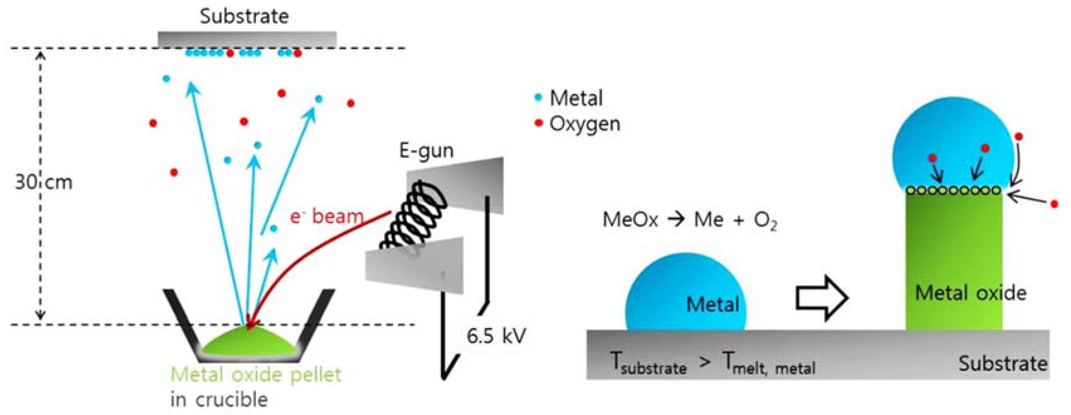
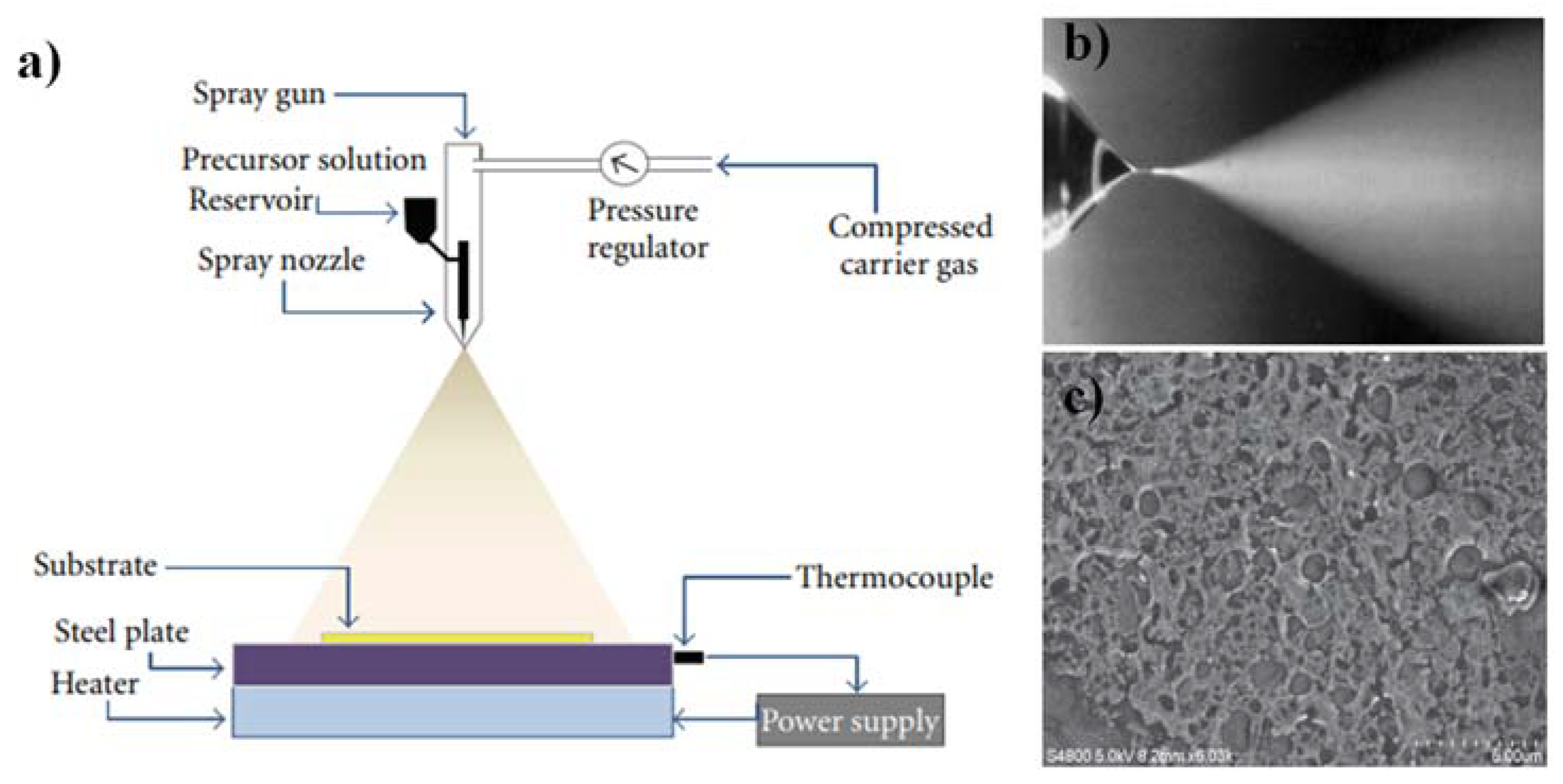
Several eye-catching techniques have been developed to implement high-quality optical thin films for light-guiding applications. Thin films are the foundation for innovative technologies in various areas, including optical devices, environmental applications, telecommunications devices, and energy storage devices. The morphology and reliability of thin films are critical issues in all applications. Deposition techniques have a major influence on thin-film morphology. Physical and chemical deposition methods can be used to deposit high-quality thin films. A thin film is a thin layer of material with a thickness ranging from a few nm to a few μm. Thin films, like all materials, are classified as amorphous or polycrystalline based on the preparation conditions and the quality of the target material. Glass WGs display highly attractive properties due to the straightforward technology, the low propagation losses, and the flexible index matching to glass fibers. It is highly desirable to have low-loss glasses, reliable and enabling low-cost WG fabrication procedures. An overall requirement is that manufacturing technologies are proficient in high yield, and have guaranteed duplicability within the quantified tolerances, and fundamentally low operating costs.

  • sol-gel dip-coating method
  • chemical vapor deposition
  • silica-titania waveguide platform
  • ion exchange

1. Thin-Film Deposition Techniques

Several physical and chemical deposition methods have been used to manufacture nanostructured thin films over the last two decades [1]. Both approaches have some benefits over traditional techniques and exhibit promising potential for the deposition process. Thin film technology requires the deposition of new transparent materials on conducting and non-conducting substrates at low temperatures. A thin film layer is a material with a thickness ranging from a fraction of a nanometer to a micrometer [2].

1.1. Physical Vapor Deposition Techniques (PVD)

Thermal evaporation method [3], electron beam evaporation [4], pulsed laser evaporation [5], molecular beam epitaxy [6], ion plating [7] and activated reactive evaporation [8] are all examples of PVD methods. This deposition process aims to move atoms from a source to a substrate, where film-forming and growth can happen independently. However, there are some disadvantages, such as the need for a tightly controlled vacuum environment and expensive instrumentation. PVD is a vaporization coating technique that requires an atomic-level material transfer. It is a vacuum-based process in which vaporized material from a source is transferred through a vacuum or low-pressure gas atmosphere to a substrate, where it condenses.
A.
Vacuum
Electron beam (E-beam) evaporation is a type of PVD in which a charged tungsten filament emits an E-beam that bombards a target anode in a vacuum and allows atoms from the target to transition to the gaseous state. The atoms then solidify, leaving a thin anode material layer on everything in the vacuum chamber. E-beam deposition achieves a high deposition rate (0.1 μm/min to 100 μm/min) at low substrate temperatures while optimizing material utilization [1]. In addition, the deposition process allows for flexible tailoring of film structure and morphology, as well as the other desired material properties like dense coating, high thermal performance, low contamination, high durability, and high throughput [4].
The deposition chamber is pumped down to ~10−5 Torr pressure. Ingots or a compressed solid are utilized as the materials to be evaporated. The E-beam can be produced by thermionic emission, field electron emission, or the anodic arc method using electron guns. The E-beam is fast-tracked to high kinetic energy and is directed towards the target material. The electrons’ kinetic energy is converted to thermal energy, which increases the surface temperature of the materials, causing evaporation and deposition on the substrate. The temperature of the electrons is usually approximately 3000 °C, and they are accelerated towards the target material by a 100 kV DC voltage source. The deposition rate is determined by the starting material and the strength of the E-beam. The vapor pressure must be around 10 mTorr for adequate deposition rates. Several materials are practically hard to evaporate by thermal evaporation [9]. E-beam evaporation must be used instead to evaporate refractory metals.
In [10], the growth process of metal oxide nanostructures produced by E-beam evaporation is demonstrated. The condensed E-beam can simply decompose metal oxide sources that have a high melting point, thus forming self-catalytic metal nanodots for the vapor-liquid-solid (VLS) method. Figure 1 shows the E-beam evaporation model for the growth of metal oxide nanowire. One benefit of E-Beam Evaporation is the possibility to rotate various source materials into the electron’s path, allowing many thin films to be deposited successively without disrupting the vacuum. A wide range of materials are deposited using E-beam evaporation, which is extensively utilized for optical thin film applications ranging from laser optics and solar panels to eyeglasses and architectural glass. It offers the necessary optical, electrical, and mechanical properties. When compared to other PVD processes, E-beam evaporation has a high material use efficacy, lowering the manufacturing cost. Various high-quality thin films such as stainless steel [4], copper [11], silicon [12], silicon nitride [13], and many more [14][15][16][17] have been deposited via the E-beam deposition method.
Figure 1. Diagrams of the E-beam evaporation model for the growth of metal oxide nanowire and growth process by vapor-liquid-solid [10].
Another physical deposition method for the thin-film-coating system is pulsed-laser deposition (PLD), in which the laser beam is used to ablate the target material for depositing thin films in a vacuum chamber [18]. Different types of laser sources are used to ablate the target, such as Nd-YAG laser, KrF (248 nm), and XeCl (308 nm). When a laser beam hits a target material, it creates a plume that can be deposited on several substrates. The plume can be composed of ionized species as well as neutral and ground-state atoms. To acquire metal oxide thin films, oxygen is used in the process. The quality of thin film deposited by the PLD method is determined by various factors, including the wavelength of the laser, energy, atmospheric gas pressure, pulse size, and the target-to-substrate distance [19]. As illustrated recently, PLD has been used to deposit an extremely diverse variety of materials. The most important use of PLD in the past has been demonstrated in high-temperature superconducting thin films. The experiment revealing that PLD could be used to deposit YBa2Cu3O7−x (YBCO) films with zero resistivity at nearly 85 K triggered intensive research on the high-temperature superconductivity over the last decade, as well as on PLD in general [20]. For detailed knowledge about the PLD method, please consult [5].
B.
Sputtering techniques
Sputtering is a physical vapor deposition procedure with a high film deposition rate and low-temperature structures, making it a good technique [21][22]. It is fast and inexpensive to create thin films of alloys, metals, nitrides, carbides, and oxides [23][24][25]. The magnetron sputtering technique, which uses a magnetic field to support the process of depositing thin films onto a substrate, is the most common procedure for this technique [26]. Via the momentum transfer from the argon (Ar) ions, the particles (atoms and ions) are discharged. Electrons are confined to the magnetic field lines in magnetron sputtering. The target is bombarded with a gaseous plasma that keeps electrons and is then guided to grind down the material and expel them in the shape of neutral particles and a small portion of ions. An inactive gas such as Ar, or even an active gas, such as nitrogen, is widely used as sputter gas. The expelled particles would then settle on the substrate and form a thin layer of the target material.
Magnetron sputtering has many benefits over other methods, including uniformity, smoothness, and strong adhesion deposition over a very substantial region. The ability to select substrate and target materials with high melting points and a high deposition rate enables simple manipulation of deposited layer thickness [27]. However, the reactive sputtering method has a variety of drawbacks, including target poisoning, low deposition rates, and arcing that produces imperfections in thin films [28]. In the sputtering techniques, however, several key factors are employed to adjust the thickness of the manufactured films. The integrated pulse energy, time of deposition, pressure in the chamber, plasma gas, target-to-substrate angle, and substrate temperature are all crucial elements in diminishing dopant redistribution and defect creation during high-temperature processing. There are several types of high-quality thin films, such as boron carbon nitride [22], aluminum oxide [29], gallium oxide [30], and others [31], deposited via the magnetron sputtering technique [21]. The history of the thin-film sputter deposition process can consult the reference [32].

1.2. Chemical Deposition Techniques

In chemical deposition techniques, materials to be deposited are permitted to respond to different chemicals, thereby permitting reactions to occur in a way that high-quality thin films are successfully deposited. Chemical deposition techniques involve gas-phase and liquid-phase deposition methods as discussed in the following section.
A.
Gas-phase
Chemical vapor deposition (CVD) and flame hydrolysis deposition (FHD) techniques fall in the category of the gas-phase deposition method, which is discussed below:
A.1. CVD techniques
CVD is a deposition process that produces high-performance solid materials, usually under a vacuum. In this technique, chemical reactions between organometallic or halide compounds and other gases form the nonvolatile solid thin films that are deposited on substrates. The key difference between this method and PVD is that the material deposition on the substrate is multidirectional, while PVD is a line-of-site impingement. CVD is widely used in microfabrication processes to deposit materials in numerous forms such as epitaxial, amorphous, monocrystalline, and polycrystalline. Unlike PVD, a definite chemical reaction between a mixture of gases and the bulk surface of the material occurs in CVD, allowing the chemical decomposition of some of the components of the gas, establishing a solid coating on the surface of the substrate. In addition, this enables the structures and properties of the resulting products to be tuned [33], and several cutting-edge CVD systems and their alternates, for instance, plasma-enhanced CVD (PECVD) [34] and metal-organic CVD (MOCVD) [35], have been industrialized. Typically, high-vacuum working environments are not needed for CVD, enabling a predominant technology for electronics, optoelectronics, and biomedical applications. There are several reports on high-quality waveguide films deposited via CVD or its alternates [36][37][38].
PECVD is a technique for depositing thin films of different materials on substrates at a lower temperature than traditional CVD. It is a hybrid coating technique in which energetic electrons trigger CVD processes (100–300 eV) inside the plasma rather than thermal energy, as in traditional CVD techniques. It is a vacuum-based deposition process that works at pressures as low as 0.1 Torr, permitting film deposition at substrate temperatures as low as 350 °C. There are several publications on the PECVD technique for the deposition of fine optical layers [39][40][41]. Since PECVD needs comparatively low substrate temperatures and offers high deposition rates, the films can be deposited onto large-area substrates that cannot survive the high temperatures needed by conventional CVD techniques. Thick coating >10 μm can be deposited with a different thermal expansion coefficient without stresses developing during the cooling [42].
MOCVD is a commonly used technique for a wide variety of materials, including electronic, optoelectronic, piezoelectric, ferroelectric, and multiferroic. Precursors made up of complex metal-organic ligands of metal ions are treated as a deposition source in this method. As opposed to PVD methods, one of the major benefits of MOCVD is that the precursors are held outside the deposition chamber and can thus be refilled continuously during long deposition runs. Several precursor mixtures with varying amounts of dopants can also be made quickly and effectively. Furthermore, superconductor film growth has been achieved at high deposition rates of more than 0.5 μm/min. Additionally, numerous mixtures of various precursors can be made with varying levels of dopants very quickly and effectively. Likewise, high deposition rates of more than 0.5 μm/min have been achieved in superconductor film growth [43]. MOCVD of other materials uses rates of about 1 μm/h, so such high rates are rare. Since MOCVD precursors can be deposited over a wide area at high deposition rates, high throughput is possible, which is crucial for large-scale manufacturing.
A.2. Flame hydrolysis deposition (FHD)
An FHD process is widely used to depose the WG films since it can provide an elevated deposition rate resulting in minimal optical losses and low-stress thin films [44]. In this deposition process, vapor precursors are added in a flame and experience chemical reactions to create soot particles which are afterward thermophoretically collected to form a porous layer on a substrate. To obtain a WG core, the porous soot deposited on the substrate must form a dense glass. To prevent the mixing of the layers, sintering temperatures are preferred such that the layers adjacent to the substrate have higher viscosities for the given temperatures. These temperatures are, sadly, often sufficient to allow the dopants to volatilize on the deposit surfaces. Consequently, in the densified glass layer, dopant concentration gradients and compositional inhomogeneities are formed, producing substandard optical properties. Such issues can be reduced or eliminated if the layers can be pre-sintered during deposition. In [45], pre-sintered WG glass films are created, allowing straight WG losses to diminish from ~0.3 dB/cm to ~0.05 dB/cm. To minimize layer mixing, sintering temperatures are adjusted so that the layers closest to the substrate have greater viscosities for a specific temperature. The FHD method offers the benefits of depositing glass films at high rates with minimal losses and producing films with low strain. However, the sintering temperatures for these layers are still high enough to induce the dopants to volatilize at the deposit’s surfaces, which is a concern. As a result, in the densified glass layer, dopant concentration gradients and compositional inhomogeneities form, resulting in poor optical characteristics. These issues might be lessened or eliminated if the layers could be placed pre-sintered during laydown. Several studies on the formation of low-loss planar WGs utilizing the FHD process have already been reported [44][46][47][48].
B.
Liquid-phase deposition
Liquid-phase deposition (LPD) is a distinctive soft solution process achieved by uncomplicated techniques. The two most widely used methods are spray pyrolysis and the sol-gel method.
B.1. Spray pyrolysis method
Spray pyrolysis is a method for preparing thin and thick films, ceramic coatings, and powders currently being researched [49]. Unlike many other film deposition techniques, it represents a very simple and relatively cost-effective processing method, especially concerning equipment costs. In this method, a thin film is deposited by spraying a solution on a heated surface where the constituents react to form a chemical compound [50]. Chemical reactants are chosen so that products other than the compounds required are volatile at the deposition temperature. It provides an incredibly simple technique to prepare films of any composition. Researchers have used this method to develop high-quality thin films which can be employed in different optical components [51][52][53][54]. Spray pyrolysis, on the other hand, has the fatal flaw of forming porous and/or hollow-structured particles [55][56]. A lot of research has gone into solving this problem [57][58]. The impact of salt solubility and physical properties on the morphology of zirconia particles made from five different salts was examined, finding that those made from precursor solutions with lower initial relative solution saturations established solid ZrO2 particles, while others formed hollow ones [59]. The inclusion of H2O2 in the ZrO2 particle preparation process aided solid particle production by slowing the breakdown reaction and preventing the development of the surface crust [60]. By introducing a stable colloidal solution into spray pyrolysis, multicomponent oxide particles with a spherical and dense shape were formed, in which the colloidal seed triggered the volume precipitation of droplets by serving as nucleation seeds [61].
Spray pyrolysis does not necessitate the use of costly substrates or chemicals. Instead, the process has been used for depositing thick films, porous films, and powder products. Using this flexible approach, even multilayered films can be effortlessly prepared. In the glass industry and solar cell production, spray pyrolysis has been used for many decades [50]. An atomizer, precursor solution, substrate heater, and temperature controller are all typical components of spray pyrolysis equipment. The schematic illustration of the spray pyrolysis process is shown in Figure 2a [51]. For the readers interested in a detailed study of this method, please consult [50]. The magnified image of the spray nozzle spraying methanol containing a small amount of HCL is shown in Figure 2b [62]. In [51], a homemade spray pyrolysis technique is used to prepare SnO2 thin films by utilizing aqueous solutions of SnCl4·5H2O. The FESEM micrograph of SnO2 thin film is shown in Figure 2c. The deposited thin film shows pores on the surface containing nanoparticles.
Figure 2. (a) The schematic of the spray pyrolysis setup [51], (b) Cone-jet spraying of methanol containing a small amount of HCL. Reprinted with permission from [62], (c) FESEM micrograph of SnO2 thin film [51].
B.2. Sol-gel method
The sol-gel method, which involves a suspension of colloidal particles, was invented at the dawn of chemistry. The groundbreaking work of Ebelmen (a French chemist) in the 1800s is credited with establishing a sol-gel synthesis of silicon tetra isoamyl oxide from silicon tetrachloride and isoamyl alcohol [63]. The latter study included the synthesis of boron amyloxide, boron ethoxide, and boron methoxide using isoamyl alcohol, ethanol, and methanol, respectively, with boron trichloride [63]. The sol-gel method is a wet chemical method for creating thin-film coatings. Its key benefits are the overall low cost of the procedure relative to more conventional processes such as CVD and PVD, as well as the ability to adapt the composition and properties of thin films to adjust the requirements of the anticipated application [64].
Thin-film coating methods must fulfill the requirements of complete control of film thickness to be successfully used in integrated optics. As a result, thickness management is critical for thin-film development processes in general, and sol-gel is no exception. It has been indicated that the final thickness is primarily determined by coating speed, angle of inclination, and sol concentration. Besides, sol viscosity, density, and liquid-vapor surface tension can also influence the final heat-treated thickness [65]. According to [66], the coating process must be carried out in a cleanroom environment to acquire sol-gel thin films of high optical quality. In [67], a three-step sol-gel process was established to make organic dye-doped thin films with customized porosity for applications in chemical sensing and optoelectronics. Moreover, sol-gel-derived ceramic films are also presented in [68]. More significant works on the sol-gel method can be found here [69][70][71][72][73][74][75][76][77][78]. To understand the popularity of the sol-gel and other traditional methods, scholars have plotted the number of research papers published on the sol-gel method, CVD, and RF-sputtering from the year 1990 to 2021, as shown in Figure 3. The data has been taken from the Scopus database, which is one of the authentic databases like Web of Science and Google Scholar. From 1990 to 2004, quite intensive research was conducted on CVD while the sol-gel method was still growing. After 2004, the sol-gel method gained more recognition for the deposition of high-quality thin films. The RF-sputtering method is also widely used in research but does not seem to be as prevalent as the other two methods.
Figure 3. The number of publications related to CVD, RF-sputtering, and sol-gel method, indexed in the Scopus database. The keywords “sol-gel dip coating method”, “Chemical vapor deposition” and “RF-sputtering” were used during the search.

2. Refractive Index Modification Methods

The refractive index (RI) of a material is a number that describes how the light will propagate through it. Light travels at different speeds in the materials having different RI, which can be changed by modifying the density of the material.

2.1. Ion Exchange Process

Ion exchange is a primeval method focused on replacing an ion existing in the glass (typically Na+) with another ion (e.g., Ag+, K+, and Li+) typically provided by a salt melt [79]. It dates to the first era as a technique for painting glass: it seems that Egyptians previously utilized it in the sixth century to embellish plates and vessels with a brownish-yellow color. The Moors used this method to dye the window glass of their palaces in Spain a few centuries later. In the 1960s, the solidification of the glass surface by ion-exchange transformed into a routine industrial procedure. Since the early 1970s, the appropriateness of ion exchange technology for the development of optical WGs in glass has been known as the groundbreaking works of Izawa and Nakagome [80] and Giallorenzi et al. [81] demonstrated techniques to benefit from the upsurge in the RI of integrated optics created by replacing the Na+ with another ion having higher electronic polarizability, for instance, silver (Ag).
Glass is a well-known optical medium, and glass WGs offer several benefits, notably inexpensive material costs, compliance with optical fibers, low propagation loss and birefringence, and good stability and durability. Ion exchange as a fabrication method offers convenience and cost savings because it does not require complex production equipment. It supports batch processing making it adaptable to a wide range of applications. The ion exchange method has also been shown to be suitable for the industrial manufacture of WG components; however, unique fabrication criteria for modules that will be used in the field must be met. After more than 10 years into ion-exchanged WGs, interest has steadily evolved, and basic demonstrations of the practicability of single-mode devices and the process’ adaptability have laid the groundwork for the technology’s prospects, such as a serious commercial production possibility frontier. Findakly examined the state of ion-exchanged glass WG available technology [82].

2.2. Ion Implantation

Ion implantation has shown to be an effective method for manufacturing optical WGs in different substrates [83][84]. In the instance of light ions being inserted, the physical density of the substrate is decreased by the damage instigated by nuclear collisions during implantation. As a result, the region with a RI lower than the substrate can function as an optical barrier that allows the light confinement in a thin layer between the surface of the substrate and the optical barrier. However, this optical confinement can be somewhat weak, and the alleged tunneling effect may occur, resulting in the energy leakage of the propagating light. To diminish light leakage to the substrate through the optical barrier, multiple-energy implants are frequently employed to extend the barrier width [85]. Heavy ions, on the other hand, may upsurge the physical density and polarizability of the substrate, which raises the RI of the implanted region bounded by the region with a lower RI, resulting in a typical optical WG. The exact precision of implantation depth and the number of doped ions employed are two main benefits of employing ion implantation. The implantation depth is proportional to the acceleration voltage, which is generally 10–100 keV, while the ion current may be used to measure the number of ions (called the dosage). The ion implantation process is complicated, and the readers who seek in-depth knowledge on this topic are referred to [86].

2.3. Femtosecond-Laser Writing

Integrated optics can be more readily miniaturized and incorporated with micro-electronics resulting in accurate and exceedingly integrated systems, contrary to many optical fiber technologies. In 1996, femtosecond (fs) laser writing was first established and had been thoroughly investigated ever since [87]. Due to its ability to swiftly and flexibly direct the inscription of the complex structures with satisfactory accuracy, fs-laser WG writing in the glass is an encouraging method for integrated optics [88]. Photolithography and FIB micromachining, on the other hand, are slower. In addition, materials, including glasses [89][90], crystals [91][92], and polymers [93][94], WG structures can now be written on directly. Compared to the most popular techniques for the development of WG, fs-laser writing has the advantages of quick production, versatility in WG design, high three-dimensional accuracy, and easy integration of the resulting WG structures with optical fiber E-beam lithography and PECVD.
It is interesting to develop integrated photonics WG sensors that do not involve any etching or complex fabrication procedures. For that reason, the WG should be written near the surface of the substrate. In most previous studies [95][96][97], the WGs were embedded inside the glass substrate via fs-laser writing. However, there are still a few reported studies on the laser-written WGs near the surface of the substrate [98][99][100]. This situation is mostly due to the ablation of glass that happens near the surface while focusing. Writing near-surface WGs is inspired by the desire to allow light to interact with the ambient medium to create integrated sensors in glass chips. Fast fabrication, flexibility in WG design, high spatial precision (i.e., limited by beam quality, wavelength, and polarization), and simple integration of the manufactured WGs with fiberized modules are all advantages of fs-laser direct writing over the most common methods, EBL and PECVD.

This entry is adapted from the peer-reviewed paper 10.3390/ma15134591

References

  1. Jilani, A.; Abdel-Wahab, M.S.; Hammad, A.H. Advance deposition techniques for thin film and coating. In Modern Technologies for Creating the Thin Film Systems and Coatings; IntechOpen: London, UK, 2017; pp. 137–149.
  2. Hao, R.; Zhu, L.; Li, Z.; Fang, F.; Zhang, X. A Miniaturized and fast system for thin film thickness measurement. Appl. Sci. 2020, 10, 7284.
  3. Boolchandani, S.; Srivastava, S.; Vijay, Y.K. Preparation on InSe thin films by thermal evaporation method and their characterization: Structural, optical, and thermoelectrical properties. J. Nanotechnol. 2018, 2018, 9380573.
  4. Ali, N.; Teixeira, J.A.; Addali, A.; Saeed, M.; Al-Zubi, F.; Sedaghat, A.; Bahzad, H. Deposition of stainless steel thin films: An electron beam physical vapour deposition approach. Materials 2019, 12, 571.
  5. Ogugua, S.N.; Ntwaeaborwa, O.M.; Swart, H.C. Latest development on pulsed laser deposited thin films for advanced luminescence applications. Coatings 2020, 10, 1078.
  6. Opel, M.; Geprägs, S.; Althammer, M.; Brenninger, T.; Gross, R. Laser molecular beam epitaxy of ZnO thin films and heterostructures. J. Phys. D Appl. Phys. 2013, 47, 034002.
  7. Martin, P.M. Handbook of deposition technologies for films and coatings (Third edition). In Science, Applications and Technology; Elsevier Inc.: Amsterdam, The Netherlands, 2010; pp. 297–313.
  8. Randhawa, H.; Bunshah, R.; Brock, D.; Basol, B.; Stafsudd, O. Preparation of CuxS thin films by activated reactive evaporation technique. Sol. Energy Mater. 1982, 6, 445–453.
  9. Paul, R.; Hossain, M.; Muktadir, M.; Faisal, K. Fabrication of a cost effective thermal evaporation system for thin film deposition. In Proceedings of the 4th International Conference on Advances in Electrical Engineering (ICAEE), Dhaka, Bangladesh, 28–30 September 2017; pp. 703–706.
  10. Yu, H.K.; Lee, J.-L. Growth mechanism of metal-oxide nanowires synthesized by electron beam evaporation: A self-catalytic vapor-liquid-solid process. Sci. Rep. 2014, 4, 6589.
  11. Komalakrishna, H.; Augustin, A.; Udaya, B.K. Electron beam deposition of copper thin film on Aluminium substrate and its characterization. Am. J. Mater. Sci. 2015, 5, 19–24.
  12. Sharma, P.; Tripathi, N.; Gupta, N. Nanocrystalline silicon thin film prepared by e-beam evaporation for display application. J. Mater. Sci. Mater. Electron. 2016, 28, 3891–3896.
  13. Katzer, D.S.; Meyer, D.J.; Storm, D.F.; Nepal, N.; Wheeler, V.D. Silicon nitride thin films deposited using electron-beam evaporation in an RF plasma MBE system. J. Vac. Sci. Technol. B Nanotechnol. Microelectron. Mater. Process. Meas. Phenom. 2014, 32, 02C117.
  14. Souk, J.H.; O’Hanlon, J.F.; Angillelo, J. Characterization of electron-beam deposited tungsten films on sapphire and silicon. J. Vac. Sci. Technol. A 1985, 3, 2289.
  15. Sontheimer, T.; Becker, C.; Ruske, F.; Klimm, C.; Bloeck, U.; Gall, S.; Kunz, O.; Young, T.; Egan, R.; Hupkes, J.; et al. Challenges and opportunities of electron beam evaporation in the preparation of poly-Si thin film solar cells. In Proceedings of the 2010 35th IEEE Photovoltaic Specialists Conference, Honolulu, HI, USA,, 20–25 June 2010; pp. 000614–000619.
  16. Sidqi, N.; Clark, C.; Buller, G.S.; Thalluri, G.K.V.V.; Mitrofanov, J.; Noblet, Y. Comparative study of dielectric coating materials for micro-cavity applications. Opt. Mater. Express 2019, 9, 3452–3468.
  17. Shamala, K.; Murthy, L.; Rao, K.N. Studies on optical and dielectric properties of Al2O3 thin films prepared by electron beam evaporation and spray pyrolysis method. Mater. Sci. Eng. B 2004, 106, 269–274.
  18. Ashfold, M.N.R.; Claeyssens, F.; Fuge, G.M.; Henley, S.J. Pulsed laser ablation and deposition of thin films. Chem. Soc. Rev. 2003, 33, 23–31.
  19. Rao, M.C. Pulsed laser deposition—Ablation mechanism and applications. Int. J. Mod. Phys. Conf. Ser. 2013, 22, 355–360.
  20. Snigirev, O.; Chukharkin, M.; Porokhov, N.; Rusanov, S.Y.; Kashin, V.V.; Tsvetkov, V.B.; Kalabukhov, A.; Winkler, D. Pulsed laser deposition of thin YBCO films on faceted YSZ single crystal fibers. In Journal of Physics: Conference Series; IOP Publishing: Bristol, UK, 2014; Volume 507.
  21. Gulkowski, S.; Krawczak, E. RF/DC magnetron sputtering deposition of thin layers for solar cell fabrication. Coatings 2020, 10, 791.
  22. Zagho, M.M.; Dawoud, H.D.; Bensalah, N.; Altahtamouni, T.M. A brief overview of RF sputtering deposition of boron carbon nitride (BCN) thin films. Emergent Mater. 2018, 2, 79–93.
  23. Khan, N.A.; Akhavan, B.; Zhou, C.; Zhou, H.; Chang, L.; Wang, Y.; Liu, Y.; Fu, L.; Bilek, M.M.; Liu, Z. RF magnetron sputtered AlCoCrCu0.5FeNi high entropy alloy (HEA) thin films with tuned microstructure and chemical composition. J. Alloy. Compd. 2020, 836, 155348.
  24. Srivastava, P.K.; Vankar, V.D.; Chopra, K.L. R.F. magnetron sputtered tungsten carbide thin films. Bull. Mater. Sci. 1986, 8, 379–384.
  25. Kylián, O.; Shelemin, A.; Solař, P.; Pleskunov, P.; Nikitin, D.; Kuzminova, A.; Štefaníková, R.; Kúš, P.; Cieslar, M.; Hanuš, J.; et al. Magnetron sputtering of polymeric targets: From thin films to heterogeneous metal/plasma polymer nanoparticles. Materials 2019, 12, 2366.
  26. Subbarayudu, S.; Madhavi, V.; Uthanna, S. Growth of MoO3 films by RF magnetron sputtering: Studies on the structural, optical, and electrochromic properties. Int. Sch. Res. Not. 2013, 2013, 806374.
  27. Abdullah, S.; Nafarizal, N.; Sahdan, M.Z. Influence of Oxygen flow rate on the characteristics of the tungsten oxide using RF magnetron sputtering. Appl. Mech. Mater. 2015, 773–774, 657–661.
  28. Sproul, W.; Christie, D.; Carter, D. Control of reactive sputtering processes. Thin Solid Films 2005, 491, 1–17.
  29. Chen, S.; Tao, L.; Zeng, L.; Hong, R. RF magnetron sputtering aluminum oxide film for surface passivation on crystalline silicon wafers. Int. J. Photoenergy 2013, 2013, 792357.
  30. Mobtakeri, S.; Akaltun, Y.; Özer, A.; Kılıç, M.; Tüzemen, E.; Gür, E. Gallium oxide films deposition by RF magnetron sputtering; a detailed analysis on the effects of deposition pressure and sputtering power and annealing. Ceram. Int. 2020, 47, 1721–1727.
  31. Nur-E-Alam, M.; Lonsdale, W.; Vasiliev, M.; Alameh, K. Application-Specific oxide-based and metal–dielectric thin-film materials prepared by radio frequency magnetron sputtering. Materials 2019, 12, 3448.
  32. Greene, J.E. Review Article: Tracing the recorded history of thin-film sputter deposition: From the 1800s to 2017. J. Vac. Sci. Technol. A Vac. Surf. Films 2017, 35, 05C204.
  33. Lin, L.; Deng, B.; Sun, J.; Peng, H.; Liu, Z. Bridging the gap between reality and ideal in chemical vapor deposition growth of graphene. Chem. Rev. 2018, 118, 9281–9343.
  34. Woehrl, N.; Ochedowski, O.; Gottlieb, S.; Shibasaki, K.; Schulz, S. Plasma-enhanced chemical vapor deposition of graphene on copper substrates. AIP Adv. 2014, 4, 047128.
  35. Cohen, A.; Patsha, A.; Mohapatra, P.K.; Kazes, M.; Ranganathan, K.; Houben, L.; Oron, D.; Ismach, A. Growth-etch metal-organic chemical vapor deposition approach of WS2 atomic layers. ACS Nano 2021, 15, 526–538.
  36. Okada, H.; Baba, M.; Furukawa, M.; Yamane, K.; Sekiguchi, H.; Wakahara, A. Formation of SiO2 film by chemical vapor deposition enhanced by atomic species extracted from a surface-wave generated plasma. AIP Conf. Proc. 2017, 1807, 020006.
  37. Matsuura, Y.; Harrington, J.A. Hollow glass waveguides with three-layer dielectric coating fabricated by chemical vapor deposition. J. Opt. Soc. Am. A 1997, 14, 1255–1259.
  38. Matsuura, Y.; Harrington, J.A. Infrared hollow glass waveguides fabricated by chemical vapor deposition. Opt. Lett. 1995, 20, 2078–2080.
  39. Gismatulin, A.A.; Kamaev, G.N.; Kruchinin, V.N.; Gritsenko, V.A.; Orlov, O.M.; Chin, A. Charge transport mechanism in the forming-free memristor based on silicon nitride. Sci. Rep. 2021, 11, 2417.
  40. Bigiani, L.; Barreca, D.; Gasparotto, A.; Andreu, T.; Verbeeck, J.; Sada, C.; Modin, E.; Lebedev, O.I.; Morante, J.R.; Maccato, C. Selective anodes for seawater splitting via functionalization of manganese oxides by a plasma-assisted process. Appl. Catal. B Environ. 2020, 284, 119684.
  41. Blout, A.; Pulpytel, J.; Mori, S.; Arefi-Khonsari, F.; Méthivier, C.; Pailleret, A.; Jolivalt, C. Carbon nanowalls functionalization for efficient O2 reduction catalyzed by laccase using design of experiment. Appl. Surf. Sci. 2021, 547, 149112.
  42. Lusk, D.; Gore, M.; Boardman, W.; Casserly, T.; Boinapally, K.; Oppus, M.; Upadhyaya, D.; Tudhope, A.; Gupta, M.; Cao, Y.; et al. Thick DLC films deposited by PECVD on the internal surface of cylindrical substrates. Diam. Relat. Mater. 2008, 17, 1613–1621.
  43. Selvamanickam, V.; Xie, Y.; Reeves, J.; Chen, Y. MOCVD-Based YBCO-Coated Conductors. MRS Bull. 2004, 29, 579–582.
  44. Ruano, J.M.; Benoit, V.; Aitchison, J.S.; Cooper, J.M. Flame hydrolysis deposition of glass on silicon for the integration of optical and microfluidic devices. Anal. Chem. 2000, 72, 1093–1097.
  45. Tandon, P.; Boek, H. Experimental and theoretical studies of flame hydrolysis deposition process for making glasses for optical planar devices. J. Non-Cryst. Solids 2003, 317, 275–289.
  46. Kilian, A.; Kirchof, J.; Przyrembel, G.; Wischmann, W. Birefringence free planar optical waveguide made by flame hydrolysis deposition (FHD) through tailoring of the overcladding. J. Light. Technol. 2000, 18, 193–198.
  47. Holmes, C.; Gates, J.C.; Smith, P.R. Planarised optical fiber composite using flame hydrolysis deposition demonstrating an integrated FBG anemometer. Opt. Express 2014, 22, 32150–32157.
  48. Zhang, L.; Xie, W.; Wu, Y.; Xing, H.; Li, A.; Zheng, W. Optical and surface properties of SiO2 by flame hydrolysis deposition for silica waveguide. Opt. Mater. 2003, 22, 283–287.
  49. Saha, J.K.; Bukke, R.N.; Mude, N.N.; Jang, J. Significant improvement of spray pyrolyzed ZnO thin film by precursor optimization for high mobility thin film transistors. Sci. Rep. 2020, 10, 8999.
  50. Perednis, D.; Gauckler, L.J. Thin Film Deposition Using Spray Pyrolysis. J. Electroceramics 2005, 14, 103–111.
  51. Patil, G.E.; Kajale, D.D.; Gaikwad, V.B.; Jain, G.H. Spray Pyrolysis Deposition of Nanostructured Tin Oxide Thin Films. ISRN Nanotechnol. 2012, 2012, 275872.
  52. Cho, J.; Hwang, S.; Ko, D.-H.; Chung, S. Transparent ZnO Thin-Film Deposition by Spray Pyrolysis for High-Performance Metal-Oxide Field-Effect Transistors. Materials 2019, 12, 3423.
  53. Filipovic, L.; Selberherr, S.; Mutinati, G.C.; Brunet, E.; Steinhauer, S.; Köck, A.; Teva, J.; Kraft, J.; Siegert, J.; Schrank, F. Methods of simulating thin film deposition using spray pyrolysis techniques. Microelectron. Eng. 2014, 117, 57–66.
  54. Ramadhani, M.F.; Pasaribu, M.A.H.; Yuliarto, B. Nugraha Fabrication of ZnO nanorod using spray-pyrolysis and chemical bath deposition method. AIP Conference Proceedings 2014, 1586, 74–77.
  55. Gurav, A.; Kodas, T.; Pluym, T.; Xiong, Y. Aerosol Processing of Materials. Aerosol Sci. Technol. 1993, 19, 411–452.
  56. Leong, K. Morphological control of particles generated from the evaporation of solution droplets: Theoretical considerations. J. Aerosol Sci. 1987, 18, 511–524.
  57. Ju, S.H.; Hong, S.K.; Jang, H.C.; Kang, Y.C. Fine size cobalt oxide powders prepared by spray pyrolysis using two types of spray generators. J. Ceram. Soc. Jpn. 2007, 115, 507–510.
  58. Lengyel, M.; Atlas, G.; Elhassid, D.; Luo, P.; Zhang, X.; Belharouak, I.; Axelbaum, R. Effects of synthesis conditions on the physical and electrochemical properties of Li1.2Mn0.54Ni0.13Co0.13O2 prepared by spray pyrolysis. J. Power Sources 2014, 262, 286–296.
  59. Zhang, S.-C.; Messing, G.L.; Borden, M. Synthesis of solid, spherical zirconia particles by spray pyrolysis. J. Am. Ceram. Soc. 1990, 73, 61–67.
  60. Cho, S.-Y.; Kim, I.-T.; Kim, D.-Y.; Park, S.J.; Kim, B.-K.; Lee, J.-H. Effects of H2O2 on the morphology of ZrO2 powder prepared by ultrasonic spray pyrolysis. Mater. Lett. 1997, 32, 271–273.
  61. Kang, Y.; Roh, H.; Park, S. Preparation of Y2O3:Eu phosphor particles of filled morphology at high precursor concentrations by spray pyrolysis. Adv. Mater. 2000, 12, 451–453.
  62. Pantano, C.; Ganan-Calvo, A.; Barrero, A. Zeroth-order, electrohydrostatic solution for electrospraying in cone-jet mode. J. Aerosol. Sci. 1994, 25, 1065–1077.
  63. Ebelmen, M. Sur les combinaisons des acides borique et silicique avec les ethers. Annl. Chim. Phys. 1846, 16, 129–166.
  64. Thor, T.; Vaclavik, J. Sol-gel preparation of silica and titania thin films. In Proceedings of the Optics and Measurement International Conference, Liberec, Czech Republic, 11 November 2016; Volume 10151.
  65. Schroeder, H. Oxide layers deposited from organic solutions. In Physics of thin films: Advances in Research and Developments; Academic Press: London, UK; New York, NY, USA, 1969; pp. 87–141.
  66. Attia, S.M.; Wang, J.; Wu, G.; Shen, J.; Jianhua, M.A. Review on sol-gel derived coatings: Process, techniques and optical applications. J. Mater. Sci. Technol. 2002, 18, 211–217.
  67. Logan, M.N.; Prabakar, S.; Brinker, C.J. Sol-Gel-Derived silica films with tailored microstructures for applications requiring organic dyes. MRS Proc. 1994, 346, 74–77.
  68. Brinker, C.; Frye, G.; Hurd, A.; Ashley, C. Fundamentals of sol-gel dip coating. Thin Solid Films 1991, 201, 97–108.
  69. Fidalgo, A.; Ilharco, L.M. The defect structure of sol–gel-derived silica/polytetrahydrofuran hybrid films by FTIR. J. Non-Cryst. Solids 2001, 283, 144–154.
  70. Parin, R.; Rigon, M.; Bortolin, S.; Martucci, A.; Del Col, D. Optimization of hybrid sol-gel coating for dropwise condensation of pure steam. Materials 2020, 13, 878.
  71. Acosta, S.; Ayral, A.; Guizard, C.; Lecornec, C.; Passemard, G.; Moussavi, M. Sol-Gel derived silica layers for low-k dielectrics applications. MRS Proc. 2000, 612, D5.26.1–D5.26.6.
  72. Boudot, M.; Gaud, V.; Louarn, M.; Selmane, M.; Grosso, D. Sol–Gel based hydrophobic antireflective coatings on organic substrates: A detailed investigation of ammonia vapor treatment (AVT). Chem. Mater. 2014, 26, 1822–1833.
  73. Kim, T.; Song, K. Low-temperature preparation of superhydrophilic coatings using tetraethoxysilane and colloidal silica by sol-gel method. Colloids Surf. A Physicochem. Eng. Asp. 2022, 647, 129105.
  74. Hasaneen, M.; Shalaby, M.; Yousif, N.; Diab, A.; El Agammy, E. Structural and optical properties of transparent conducting oxide Cd1-xCrxO thin films prepared by the sol-gel dip-coating method. Mater. Sci. Eng. B 2022, 280, 115703.
  75. Niazmand, M.; Maghsoudipour, A.; Alizadeh, M.; Khahpour, Z.; Kariminejad, A. Effect of dip coating parameters on microstructure and thickness of 8YSZ electrolyte coated on NiO-YSZ by sol-gel process for SOFCs applications. Ceram. Int. 2022, 48, 16091–16098.
  76. Esfahani, M.B.; Eshaghi, A.; Bakhshi, S.R. Transparent hydrophobic, self-cleaning, anti-icing and anti-dust nano-structured silica based thin film on cover glass solar cell. J. Non-Cryst. Solids 2022, 583, 121479.
  77. Beldjebli, O.; Bensaha, R.; Panneerselvam, P. Effect of both sn doping and annealing temperature on the properties of dip-coated nanostructured TiO2 thin films. J. Inorg. Organomet. Polym. Mater. 2022, 32, 1624–1636.
  78. Both, J.; Szabo, G.; Katona, G.; Muresan, L. Tannic acid reinforced sol-gel silica coatings for corrosion protecion of zinc substrates. Mater. Chem. Phys. 2022, 282, 125912.
  79. Rogozinski, R.; Karasinski, P. Optical waveguides produced in ion exchange process from the solutions of AgNO3-NaNO3 for planar chemical amplitude sensors. Opto-Electron. Rev. 2005, 13, 229–238.
  80. Izawa, T.; Nakagome, H. Optical waveguide formed by eletrically induced migration of ions in glass plates. Appl. Phys. Lett. 1972, 21, 584–586.
  81. Giallorenzi, T.; West, E.; Kirk, R.; Ginther, R.; Andrews, R. Optical waveguides formed by thermal migration of ions in glass. Appl. Opt. 1973, 12, 1240–1245.
  82. Findakly, T. Glass Waveguides by Ion Exchange: A Review. Opt. Eng. 1985, 24, 242244.
  83. Namba, S.; Aritome, H.; Nishimura, T.; Masuda, K.; Toyoda, K. Optical waveguides fabricated by ion implantation. J. Vac. Sci. Technol. 1973, 10, 936–940.
  84. Bi, Z.-F.; Wang, L.; Liu, X.-H.; Zhang, S.-M.; Dong, M.-M.; Zhao, Q.-Z.; Wu, X.-L.; Wang, K.-M. Optical waveguides in TiO2 formed by He ion implantation. Opt. Express 2012, 20, 6712–6719.
  85. Chandler, P.J.; Zhang, L.; Townsend, P.D. Double waveguide in LiNbO3 by ion implantation. Appl. Phys. Lett. 1989, 55, 1710–1712.
  86. Townsend, P.D.; Chandler, P.J.; Zhang, L. Optical Effects of Ion Implantation; Cambridge University Press: Cambridge, UK, 1994.
  87. Davis, K.M.; Miura, K.; Sugimoto, N.; Hirao, K. Writing waveguides in glass with a femtosecond laser. Opt. Lett. 1996, 21, 1729–1731.
  88. Gross, S.; Dubov, M.; Withford, M.J. On the use of the Type I and II scheme for classifying ultrafast laser direct-write photonics. Opt. Express 2015, 23, 7767–7770.
  89. Chen, G.Y.; Piantedosi, F.; Otten, D.; Kang, Y.Q.; Zhang, W.Q.; Zhou, X.; Monro, T.M.; Lancaster, D.G. Femtosecond-laser-written Microstructured Waveguides in BK7 Glass. Sci. Rep. 2018, 8, 10377.
  90. Ehrt, D.; Kittel, T.; Will, M.; Nolte, S.; Tünnermann, A. Femtosecond-laser-writing in various glasses. J. Non-Cryst. Solids 2004, 345–346, 332–337.
  91. Butt, M.A.; Nguyen, H.-D.; Ródenas, A.; Romero, C.; Moreno, P.; De Aldana, J.R.V.; Aguiló, M.; Solé, R.M.; Pujol, M.C.; Díaz, F. Low-repetition rate femtosecond laser writing of optical waveguides in KTP crystals: Analysis of anisotropic refractive index changes. Opt. Express 2015, 23, 15343–15355.
  92. Fedotov, S.S.; Butvina, L.N.; Okhrimchuk, A.G. Plastic deformation as nature of femtosecond laser writing in YAG crystal. Sci. Rep. 2020, 10, 19385.
  93. Pätzold, W.M.; Demircan, A.; Morgner, U. Low-loss curved waveguides in polymers written with a femtosecond laser. Opt. Express 2017, 25, 263–270.
  94. Nguyen, H.H.D.; Hollenbach, U.; Pfirrmann, S.; Ostrzinski, U.; Pfeiffer, K.; Hengsbach, S.; Mohr, J. Photo-structurable polymer for interlayer single-mode waveguide fabrication by femtosecond laser writing. Opt. Mater. 2017, 66, 110–116.
  95. Cerullo, G.; Osellame, R.; Taccheo, S.; Marangoni, M.; Polli, D.; Ramponi, R.; Laporta, P.; Silvestri, S.D. Femtosecond micromachining of symmetric wavegudies at 1.5 um by astigmatic beam focusing. Opt. Lett. 2002, 27, 1938–1940.
  96. Eaton, S.M.; Ng, M.; Osellame, R.; Herman, P.R. High refractive index contrast in fused silica waveguides by tightly focused, high-repetition rate femtosecond laser. J. Non.-Cryst. Solids 2011, 357, 2387–2391.
  97. Fletcher, L.B.; Witcher, J.J.; Troy, N.; Reis, S.T.; Brow, R.K.; Krol, D.M. Direct femtosecond laser waveguide writing inside zinc phosphate glass. Opt. Express 2011, 19, 7929–7936.
  98. Martínez, J.; Ródenas, A.; Stake, A.; Traveria, M.; Aguiló, M.; Solis, J.; Osellame, R.; Tanaka, T.; Berton, B.; Kimura, S.; et al. Harsh-Environment-Resistant OH-Vibrations-Sensitive Mid-Infrared Water-Ice Photonic Sensor. Adv. Mater. Technol. 2017, 2, 1700085.
  99. Lapointe, J.; Parent, F.; de Lima Filho, E.S.; Loranger, S.; Kashyap, R. Toward the integration of optical sensors in smartphone screens using femtosecond laser writing. Opt. Lett. 2015, 40, 5654–5657.
  100. Amorim, V.A.; Maia, J.M.; Viveiros, D.; Marques, P.V.D.S. Inscription of surface waveguides in glass by femtosecond laser writing for enhanced evanescent wave overlap. J. Opt. 2020, 22, 085801.
More
This entry is offline, you can click here to edit this entry!
ScholarVision Creations