Optical Components Used to Implement Optical Functions: History
Please note this is an old version of this entry, which may differ significantly from the current revision.
Contributor:

Deep learning has an unquenchable thirst for processing resources. Classical deep learning has silently developed a bottleneck due to the interference of electrical impulses, energy usage, and physical constraints, even though electronic parts established on silicon can still sustain it presently. Academic and corporate circles are attempting to find new approaches for resolving electrical flaws that are less computationally intensive. It has huge benefits in information transmission and OC due to its high speed of 300,000 km per second, which is 300 times faster than that of an electron, and its data-carrying capacity and variety, which is 2 × 10⁴ times greater than that of electric channels, as well as high parallelism and strong anti-interference. Switching electricity with light has emerged as a viable and sustainable work style, following the current trend.

  • Optical Component
  • Optical Functions

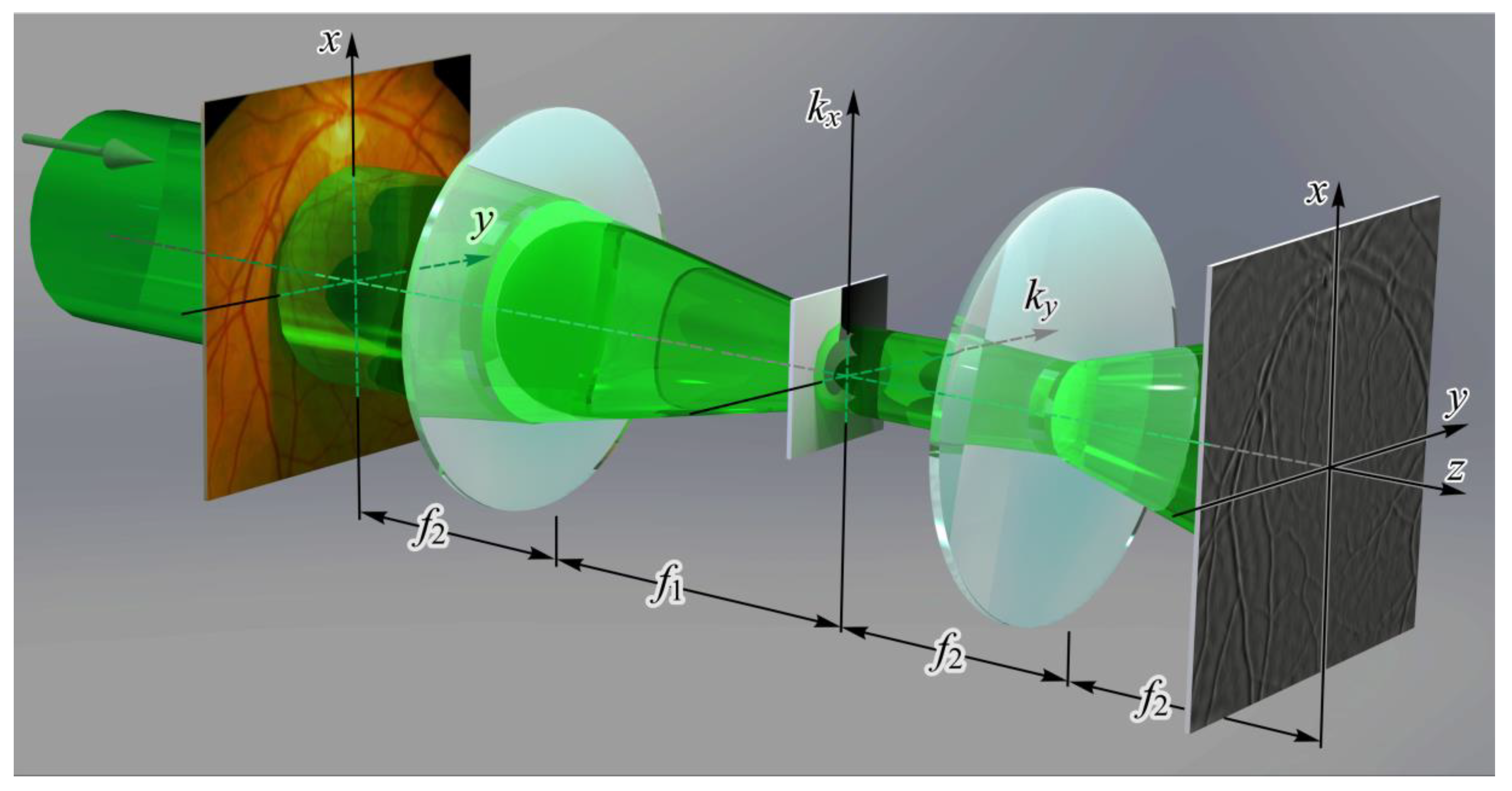
1. Spatial Light Modulator (SLM)

Light wave processing has provided useful techniques for converting data into spatially modulated coherent light waves using SLM apparatuses, allowing the creation of digital holographic images [1]. The capacity to alter the phase and amplitude of light in the far-field is one of the hologram’s most valuable qualities. The FT illustrates how a hologram (near field) interacts with its replay field (far-field). In free space, the far-field might develop at the focal point of a positive lens or an indefinite distance from the near field plane [2]. Waveforms from an existent item can be reproduced using holograms. With developments in digital technology and light wave processing, it is now feasible to compute interference patterns computationally and construct synthetic wavefronts of any shape. Computer generated hologram (CGH), diffractive optical elements (DOE), phase/amplitude masks, diffractive grating, and other terms can be used to describe these interference patterns. Because they all work on the concept of diffraction, the nomenclature is rather arbitrary.
CGHs and DOEs have historically been used to implement various optical operations in correlators as spatial filters [3][4][5]. Despite the advent of dynamically controlled SLMs, the use of DOEs in Fourier correlators remains relevant in high-energy applications [6] since they have a significantly higher damage threshold than SLM. Soifer et al. have designed a multichannel spatial optical that allows coherent light fields to be optically decomposed into a series of orthogonal functions: using angular harmonics to calculate the light field’s angular momentum [7][8][9][10][11], detection and analysis of wavefront aberrations using Zernike polynomials [12][13][14][15][16], and using the optical Karhunen–Loeve decomposition, decorrelated image characteristics may be dervied [17][18]. Relying on segmented spatial filters in the sequence of diffraction gratings, an optical approach for producing a directions field for fringed/contour pictures such as interferograms and fingerprints has been established [19][20][21][22]. To deepen focus and adjust for defocusing and chromatic aberrations, imaging systems undergo phase apodization and optical wavefront coding [23][24][25][26]. The spiral phase plate as a phase rotor filter is suggested to be used to visually realize the m-th order Hankel transform as well as to optically discriminate the light field with rotational symmetry [27]. In contrast to the commonly used 2D Hilbert transforms in image processing, the vortex spatial phase filter is utilized to execute the radial Hilbert transform, which is isotropic [28][29][30]Figure 1 shows the operation of the optical correlator with a spatial filter in the form of the spiral phase plate for the implementation of the radial Hilbert transform to contrast the image of the fundus vessels [28]. In this way, a correlation filter can be used not only for the classical task of optical detection (recognition) but also for the optical implementation of a mathematical operation such as Hilbert transform (Figure 1).
Figure 1. Illustration of the optical implementation of the radial Hilbert transform using the spiral phase plate as a spatial filter to contrast the image of the fundus vessels [28].
The SLM is an electrically programmable device that may modify light in compliance with a fixed spatial (pixel) pattern. It may typically be used to adjust the phase and/or amplitude of incoming light. As a result, SLM may easily realize phase-only, amplitude-only, or a combination of phase-amplitude [31]. Commercially available SLMs are quite “slow”, although faster ones are also known [32]. A DMD (digital micromirror device) is considered a fast analogue of SLM. DMDs show switching speed ranging from several kHz to tens of kHz (settling time for full-scale angle change is around 10 μs) [33]; however, high speed comes at the expense of limited modulation depth and diffraction efficiency [34]. Thus, in applications where high energy efficiency is not required, it is possible to use DMDs instead of SLMs. There are a variety of modulation techniques to choose from. EO-SLM is one of the most appealing and commonly utilized. Liquid crystal is used as the modulation material in EO-SLM. A micro-display is used for incident light manipulation and collecting in a liquid crystal SLM as well. This may be completed in two ways: as a transmissive display using LCD SLM technology or as a reflective display using LCoS SLM technology. The liquid crystal molecular alignment is one of the modulator’s most prominent characteristics. This might take the form of a vertical, parallel, or twisted structure. As a result, with the right polarizing optics, the incident beam of light parameters, such as amplitude, phase, or their combination, may be efficiently adjusted.
The nematic LCoS technology is a form of SLM that allows for phase-only modulation [35]. Furthermore, it belongs to the electrically addressed reflection modulator class, in which the liquid crystal is controlled by a direct and precise voltage, and the beam of the light wavefront may be adjusted as well. The LCoS SLM may be used to rebuild pictures from CGH as a diffractive modulator [36]. CGHs may be used for a variety of communication applications, and it is increasingly being used in indoor visible light communication networks [37]. Additionally, a range of optimization approaches, including the iterative Fourier transform algorithm (IFTA), linear Fourier transform (i.e., linear phase mask), simulated annealing, and the Gerchberg–Saxton algorithm, can be used to quickly construct acceptable holograms [38][39]. The beam of the light wavefront can be modified when the SLM is used as a diffractive device for reconstructing graphics from CGH.
As previously stated, LCoS displays have gained a lot of traction as potential microdisplays for a variety of SLM applications. Likewise, they have appealing and important characteristics such as excellent spatial resolution and light efficiency. As a result, they have been employed in a wide range of optical utilizations, including communication, reconfigurable interconnects [40], storage [41], diffractive optics [42], metrology [43], and quantum computing [44]. They can also be used for light wave processing and monitoring in wave shaper technology [45]. Another feature of the LCoS is that it is extremely cost-efficient and can be configured in a variety of ways. Several functionalities such as group delay ripple correction, wavelength filtering, and chromatic dispersion correction are made possible by this. In addition, LCoS technology may be used in flex grids, which has been regarded as a key component for next-generation networks [41]. The classic fixed grid with 50 GHz spacing, as regulated by the International Telecommunication Union (ITU) Telecommunication Standardization Sector (ITU-T), has a variety of drawbacks. The fixed grid has been reported to result in poor usage of the optical spectrum. Furthermore, it severely limits the system’s transmission capacity. The flex grid implementation, on the other hand, allows for the use of several modulation formats and their coexistence on a common infrastructure. They can also be multiplexed densely and effectively, which helps optical networks not only extend their reach but also increase the per-channel data rate. It is also expected that the deployment of WSS and SDM would considerably aid in the expansion of the network’s coverage and capacity [41].
Electrically addressed SLMs (EASLMs) and optically addressed SLMs (OASLMs) are two types of SLMs that differ in how data are loaded into the apparatuses [46]. The EA has been the most prominent approach in modern commercial SLMs because of the growth of electronic information technology over the last few decades. However, because data must be converted back and forth between the optical and electrical domains, EASLMs are not the greatest solution for future all-optical information processing systems. The OASLMs, on the other hand, enable light to be modulated directly by light without having to go through an electronic–optical transformation [47][48]. Additionally, OASLMs are required for a variety of all-optical purposes that EASLMs cannot handle, such as coherent to incoherent image conversion, real-time optical correlation, and parallel all-optical processing [49][50][51][52][53]. OASLMs may be built in theory using material nonlinearities, with modulation over the read light achieved by spatially precisely modifying the characteristics of the materials through nonlinear optical stimuli [54]. Natural materials, on the other hand, have insufficient nonlinearities to permit efficient “light-control-by-light” inside nanoscale volumes. This renders the apparatuses exceedingly bulky or necessitates a lot of pumping power to collect big enough nonlinear modulations, making them unsuitable for the nano-era.
The recent remarkable advancement in dynamic optical metasurface (MS) technology gives a chance to overcome the challenges and proposes a unique framework for nanoscaled SLM [55][56]. The MS can also enhance optical engagements by focusing light on nanoscale volumes, allowing for the greater control of light fields in response to external mechanical, chemical, and magnetic stimuli, for example. The ultracompact EASLMs established on MS have recently been observed relying on the active manipulation of beams of light by additional electrical fields [57]. An OASLM established on MS-OASLM is proposed in [58], with a nonlinear polarization manipulation of read light by another write light at the nanoscale as the operating mechanism. It delivers 500-line pairs/millimeter (equivalent to a pixel size of just 1 μm), which is more than 10 times greater than a standard commercial SLM. The MS-OASLM has exceptional compactness and a thickness of just 400 nm. MS-OASLMs such as this might pave the way for next-generation all-optical data processing and high-resolution display technologies.

2. Plasmonic Switches

Moore’s law is expected to surpass its physical constraints, putting modern computer systems centered on von Neumann architecture at a physical limit [59][60]. Potential alternate prospect next-generation computing approaches are necessary due to the rapidly rising development of bandwidth needs with lower power utilization. As a result of the usage of optical interconnects in high computing chips rather than electrical interlocks to minimize power consumption and increase speeds, photonic computing is expected to have a competent replacement for existing electronic computing systems. Furthermore, Si photonics has considered a leading field owing to its capacity to provide effective light modulation, light confinement, and compliance with today’s CMOS production techniques [61][62]. A decade ago, the shift from electronic to photonic systems began. Related to current material discoveries, fabrication technique advances, and more ongoing research efforts in this field, photonic interconnects and circuits have witnessed significant advancements in recent years.
Photonic logic circuits rely heavily on optical switching and modulation. Optical computations are established on photonic logic circuits. Utilizing the thermo-optic effect, free carrier dispersion effect, and Pockels electro-optic effect, intensive research in the direction of efficient optical switches, optical modulators, and optical logic circuits has been presented [63][64][65][66]. All these tools are volatile, requiring constant voltage to manage, and as a result, they consume a lot of power. Furthermore, due to their low electro-refractivity, they have long interaction durations. As a result, these apparatuses have substantial footprints, making ultra-compact designs difficult to achieve [67][68]. A novel type of material known as phase change materials (PCMs) has found considerable application in both the electronics and photonics domains in recent years [69][70]. With high-speed switching between two steady states, PCMs reveal changes in electrical and/or optical characteristics. Several photonic and plasmonic apparatuses have been proposed and investigated, including on-chip optical modulators and optical switches established on PCMs [71][72]. One of the widely used PCMs in photonic apparatuses is Ge2Sb2Te5 (GST) [73].
Even though effective energy non-volatile (NV) memory and OLGs based on PCMs have been thoroughly researched and established over the last 20 years, PCM-based photonic NV memories and photonic logic circuits have received little attention. Novel NV combinational and sequential logic circuit designs are investigated as well as NV hybrid electro-optic plasmonic circuits. The electro-optic devices are made up of a plasmonic waveguide (WG) with a mono PCM layer. Changing the phase of the PCM between amorphous to crystalline likewise changes the optical losses in the WG. Electrical threshold flipping or thermal conduction heating via externally applied radiators or the plasmonic WG metal itself as an integrated heater can be used to generate phase shift in the PCM. All OLGs, a half adder circuit, and sequential circuits may be built employing plasmonic switches as active components, as illustrated. Furthermore, the plasmonic switches and logic functions have minimal extinction ratios larger than 20 dB, are small, have little operational power, and operate at high speeds. To develop an effective architecture for logic processes, photonics, plasmonics, and electronics are merged on the same platform.
A plasmonic slot WG with PCM as an active material coating the slot WG’s surface is used in the NV hybrid electro-optic plasmonic switch [74]Figure 2a depicts the suggested plasmonic slot WG’s construction, which includes Si-Au tapered WGs, a slot in an Au film to form a plasmonic slot WG, and a PCM coating for instance GST on the slot WG’s surface. The arrangement is made up of three primary components, the first of which is a dielectric to plasmonic mode converter in the I/P region of a hybrid Si-Au tapered WG. The major optical modulation happens in the second portion, which is an MIM plasmonic slot WG covered with a thin coating of GST, and the third part is a plasmonic to dielectric mode converter in the O/P section, which uses a hybrid Au–Si tapered WG. The cross-sectional image (in the y–z plane) of the GST-coated plasmonic slot WG is shown in the left top inset of Figure 2a [74].
Figure 2. (a) The broadband NV hybrid EO plasmonic switch is shown schematically. The side view picture of the plasmonic slot WG with a thin coating of GST is shown in the inset [74], (b) The hybrid NV EO-plasmonic switch serves as the central unit in the racetrack μ-RR-based EO switch [74], (c) Normalized transmission spectra for the amorphous and crystalline phases of the PCM layer of the racetrack μ-RR-based EO switch, (d,e) The E-field mapping of the EO switch for the amorphous phase and the crystalline phase of the PCM layer at the resonance wavelength of 1558 nm, respectively [74], (f) Asymmetric MZI-based EO switch with hybrid NV EO plasmonic switch as an active component in one arm, (g) Normalized transmission band for the crystalline and amorphous phases of the PCM layer in the plasmonic switch for the asymmetric MZI based EO switch. The E-field distribution of the EO switch for the (h) amorphous phase and (i) crystalline phase of the PCM layer at the resonance wavelength of 1548 nm [74].
As illustrated in Figure 2b, the EO switch is established on a racetrack micro-ring resonator (μ-RR) with an NV hybrid EO plasmonic switch in the ring WG as an active component. The optical mode is linked to the ring through a Si WG with the same cross-section as the hybrid plasmonic switch’s Si WG. The transmission spectra for both phases are shown in Figure 2c. The optical loss in the ring is minimal when GST is in the amorphous phase. Consequently, light can pass through the RR and propagate via the optical mode. For specific wavelengths, resonance is obtained in the RR, and after a roundtrip, light coupled back to the I/P WG’s throughport undergoes a 180° outphasing in comparison to light arriving from the I/P WG’s I/P point. As a result, destructive interference develops between light flowing from the I/P point and light coupled back to the I/P WGs through the port. As a result, light departing the O/P port at resonance wavelengths is eliminated, as shown in Figure 2d. The optical mode, on the other hand, cannot travel via the ring WG due to momentous optical loss in the crystalline phase. Consequently, there is no intrusion, and optical power is sent via the O/P port, as shown in Figure 2e [74].
Established on the hybrid plasmonic switch anticipated in [74], an asymmetric MZI is depicted in Figure 2f. The asymmetric MZIs were designed using compact and low-loss Y-junction-based splitters and combiners. The I/P segment’s splitter divides the I/P power evenly between the MZI’s two arms, while the O/P section’s combiner merges the optical powers of the two arms. The asymmetric MZI’s hybrid plasmonic switch is incorporated in the sorter arm. Figure 2g–i shows the transmission spectra and field mappings of the MZI for GST amorphous and crystalline phases, respectively.

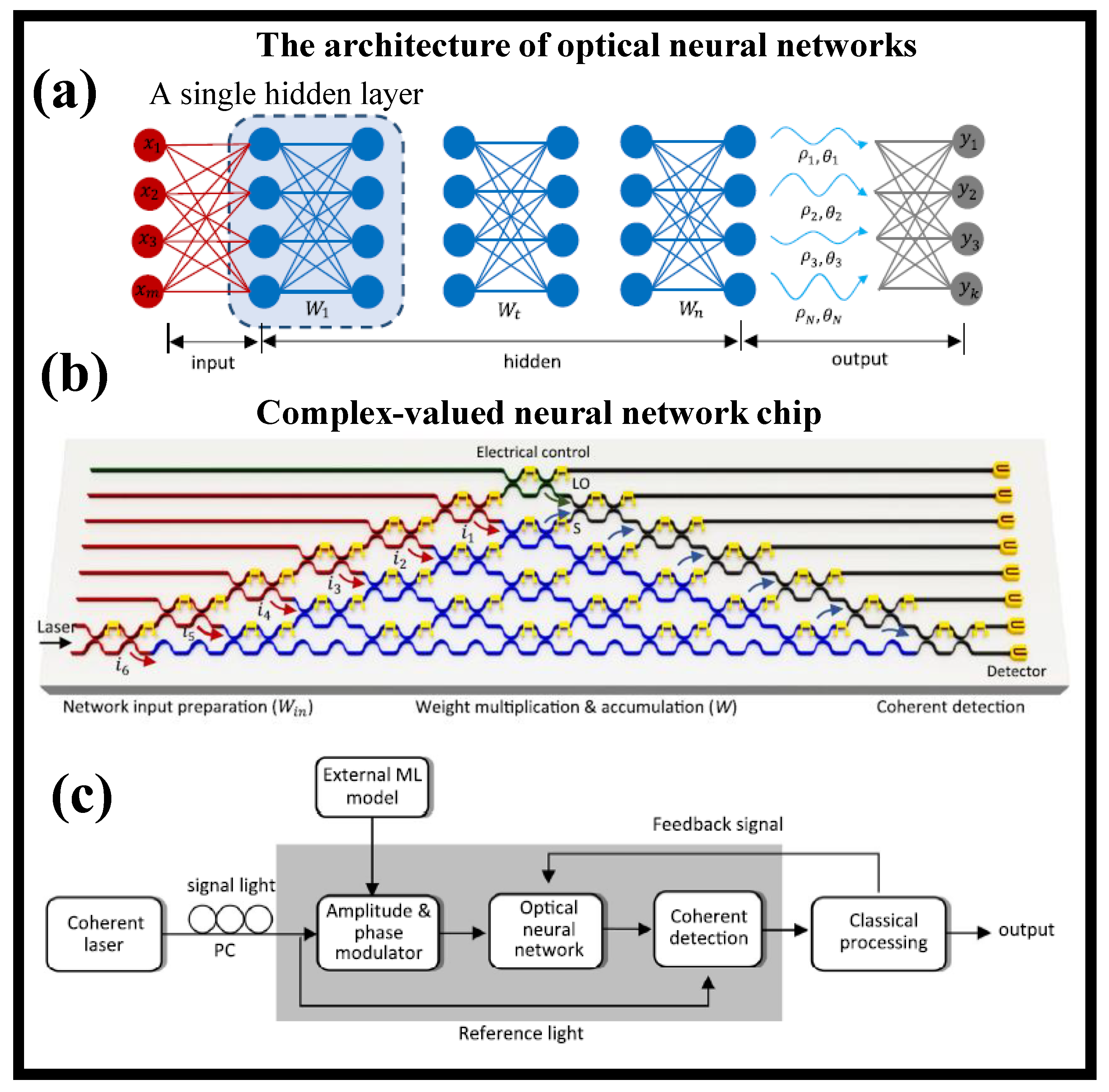
3. Neural Networks (NNs)
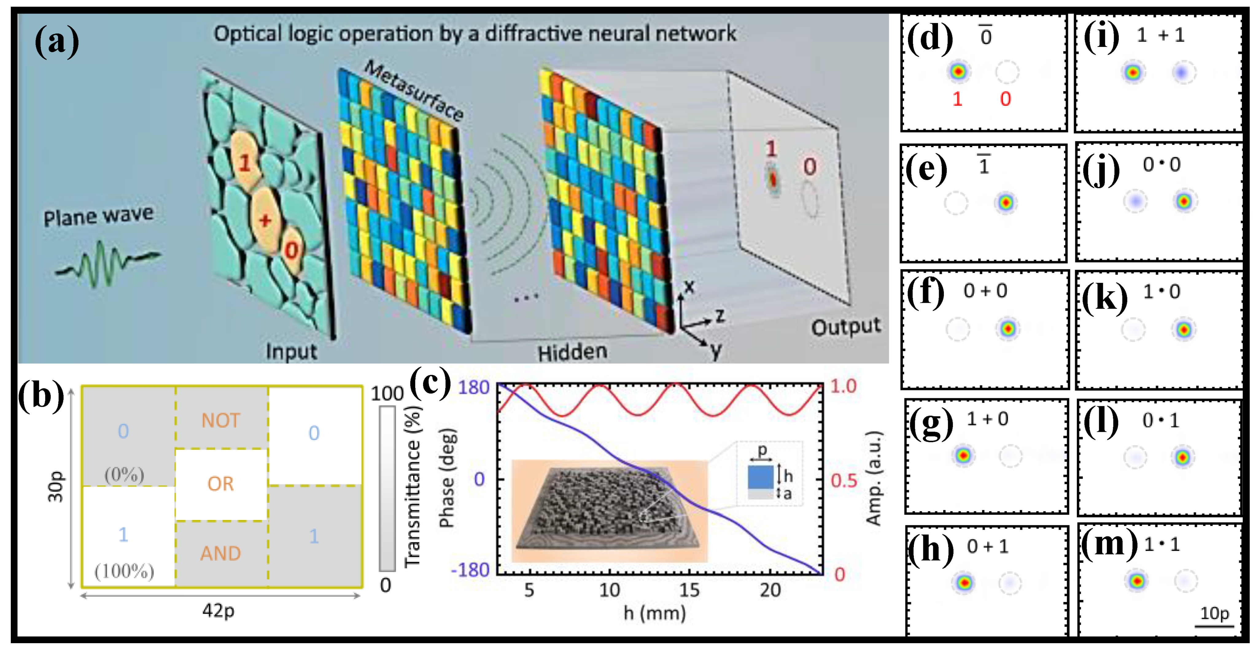
Artificial intelligence, as among the most effective areas in computer science, focuses on simulating the framework of the nervous system by constructing artificial neural networks (ANNs), which maintain connections between neurons in multiple layers of the NN and give it higher accuracy and robustness. ANN’s research has advanced significantly since the 1980s. It has also effectively solved many functional challenges for modern computers in the fields of pattern recognition, intelligent robots, automatic control, prediction and estimation, biomedicine, economy, and other fields, all while retaining better intelligence attributes. Advanced machine learning techniques, which include ANNs [75][76], have received a lot of interest because of their practical uses in important tasks such as image identification and speech processing [77]. NNs employ a lot of multiply–accumulate (MAC) operations, which puts a huge amount of pressure on current electronic computing technology (e.g., CPU, GPU, FPGA, ASIC). For MAC activities, application-specific apparatuses are recommended. Most NNs depend solely on real-valued arithmetic, even though complicated arithmetic might provide a large benefit. For example, a single complex-valued neuron with orthogonal decision boundaries can help resolve the symmetry challenge and the XOR issues, while a single real-valued neuron cannot [78]. Research indicates that complex-valued arithmetic [79] might help NNs function better by providing extensive representational capacity, quick convergence, powerful applicability, and noise-resistant memory mechanisms. Since complex numbers must be formed by two real numbers, which fuels the growth of MAC operations—the most commonly frequently utilized computationally expensive components of NN algorithms—conventional digital electronic computing platforms experience considerable slowdown when implementing algorithms utilizing complex-valued operations [80][81]. To circumvent these difficulties, it has been suggested that the computationally demanding process of building NNs be delegated to OC, which is proficient in genuinely complex-valued arithmetic [52].
Low power consumption, fast processing time, huge data storage, and intrinsic parallelism are all benefits of OC that cannot be matched by its electrical cousin. Numerous optical NN algorithms have been suggested. Photonic chip-based optical NNs, for example, have grown extremely popular due to their remarkable adaptability, scalability, and durability. This system has previously shown neuromorphic photonic weight banks [82], all-optical NNs [83], and optical reservoir computing with tremendous results [84]. On an embedded silicon photonic device, a typical fully connected NN was realized experimentally [85]. Although this optical device is established on light interference, the NN algorithms used are real-valued, negating the merits of sophisticated NNs. The optical impulses were already transformed to photocurrents before entering the accumulator, resulting in a highly parallelized optical NN accelerator established on photoelectric multiplication, which was also built for real arithmetic. On-chip training, optical nonlinear activations [86], and different NN designs are further subjects linked to optical NNs [87].
Apart from OC platforms, analogue electronic apparatuses have effectively exhibited multilayer perceptrons [88][89] and convolutional NNs as compared to more prevalent digital electronic apparatuses [90]. Some earlier research has looked at complex-valued NNs on analogue electrical apparatuses [91][92][93]. Complex-valued reservoirs also result in enhanced system dynamics and enhanced efficiency in reservoir computation. Although optical NNs can handle information in multiple degrees of freedom (e.g., magnitude and phase) using complex-valued numerical methods and acquire more effective information processing and analysis, there have been few investigations in OC platforms for integrating general-purpose and complex-valued NNs [94]. Strongly dependent on traditional deep learning algorithms developed for real-valued arithmetic on traditional electronic computers, existing optical solutions have not walked into this prospective flatland. These real-valued optical NNs are built exclusively on the intensity information of the light waves, ignoring the phase information, which eliminates one of OC’s primary advantages.
These problems were answered by designing and demonstrating an optical neural chip (ONC) that performs complex-valued arithmetic, demonstrating the benefits of chip-based complex-valued networks via OC. It has been proved that an optical neural chip (ONC) can build fully complex-valued NNs [95]. The complex-valued ONC’s system is analyzed in four contexts: basic Boolean tasks, species classification of an Iris dataset, nonlinear dataset classification (Circle and Spiral), and handwriting recognition. When referred to its real-valued equivalent, the complex-valued ONC achieves strong skillsets (i.e., precision, quick resolution, and the capacity to generate nonlinear decision boundaries). Figure 3a depicts the optical NN’s architecture, consisting of an I/P layer, many hidden layers, and an O/P layer [95]. During the initial I/P signal preparations and network growth in the complex-valued architecture, light signals are encoded and modulated both by optical magnitude and phase. Figure 3b depicts the ONC design for implementing complex-valued NNs [95]. A single-chip handles I/P preprocessing, weight multiplication, and coherence detection. The I/P signals are generated using a coherent laser (λ = 1550 nm). The ONC is simply a multiport interferometer with a special arrangement of Mach–Zehnder interferometers (MZIs). Each MZI is made up of two-beam splitter–phase shifter (BS–PS) pairs. The BS has a stable transmittance of 50:50, while the PS is thermally regulated to modify the phase. MZIs highlighted with various colors in the figure have distinct capabilities. The bottom point couples the light into the chip. The red chain of MZIs is responsible for I/P light splitting and modulation. The green MZI label distinguishes the baseline light that will be utilized for coherent detection. The on-chip light division ensures that light signals flowing through multiple optical routes are polarized similarly and have a constant relative phase. The machine learning job determines the modulation of the I/P. For jobs involving real-valued I/Ps, the amplitude of the light signals is modulated, and the relative phases between distinct pathways are reduced to 0.
Figure 3. A complex-valued coherent optical NN’s composition. (a) An I/P layer, many hidden layers, and an O/P layer make up an optical NN. During the initial I/P preparation and network evolution, the light signals are encoded and modulated by both amplitude and phase in the complex-valued architecture [95]. (b) The ONC’s diagram for implementing complex-valued networks. On a single chip, I/P preprocessing, weight multiplication, and coherence recognition are all combined. The MZIs in red are responsible for the division and modulation of the light signals (i1i6). The green MZI distinguishes the reference light that will be utilized for coherent detection later. Blue indicates the MZIs that were utilized to build the 6x6 complex-valued weight matrix. On-chip coherent tracking is established on the remaining gray designated MZIs [95]. (c) The ONC system’s process. Signal and reference light is generated using a 1550 nm coherent laser. The amplitude and phase of the signal light on each path are modified by the machine learning (ML) job. The light inference is used to perform the weighted sum process passively. The measurement findings are transferred to the electrical interface for processing, which includes activation function application and cost function computation. The modified weight matrices are then used to reprogram the ONC chip [95].
On-chip coherent tracking is based using the gray MZIs. The optical chip’s O/P light signals contain both magnitude and phase information, whereas traditional intensity monitoring systems merely retrieve magnitude data. The intensity and coherent detection are both possible with the integrated chip. The purpose of coherent tracking is to find the phase angles between both the reference and signal light. The O/P current achieved by linking photodiodes at both O/Ps in a balanced manner is I1α2AsA1cosфs, where As and A1 are the signal and reference light amplitudes, respectively. Likewise, if the baseline light is phase-shifted by π/2, the O/P current is IQα2AsA1sinфs. The фs is then calculated using the ratio of I1 and IQ, which also aids in the removal of physical noise from optical components. The activation analysis determines which detecting approach is used. A transimpedance amplifier (TIA) converts the recorded photocurrents into voltage signals, which are subsequently gathered and analyzed by a traditional processor with an analog-to-digital converter (DAC). As demonstrated in Figure 4c, feedback signals may be created and routed back to the ONC to alter chip layouts [95].

4. Diffractive NN

Prior works to OLGs focused primarily on constructive/destructive interference effects between the I/P light signals, encompassing linear [96][97][98][99] and nonlinear interference [100]. The reported works are heavily reliant on accurate positioning of the basic characteristics of two I/P light signals, the control light and/or the pump light, such as phase difference, polarization, and intensity; if the two nanowires are close to each other, as in the plasmonic logic gate, there is also a mandatory rule on the size of I/P beams of light to prevent a big false I/P. Consequently, greater tight control of I/P light may more fully actualize constructive or destructive interference, resulting in a bigger intensity contrast ratio between the two O/P optical logic states “1” and “0”, which is a critical quality to evaluate an OLG’s performance. The heavy dependency on precise I/P light management has two negative effects on the development of miniaturized OLGs. First, the substantial optical components required to perform these controls are considered, and downsizing becomes challenging. Second, because of the complexities of achieving perfect I/P light control, their performance may be unstable, and the intensity contrast ratio between two O/P logic states may become rather low in practical circumstances. It is therefore very desired for compact OLGs to eliminate these important I/P light needs. Due to the necessity of developing innovative designs for all-optical apparatuses and systems, such a goal remains an open problem that has long been sought after.
All seven fundamental optical logic operations (OLOs) are realized in a small system utilizing just plane waves as the I/P signal, thanks to a simple yet universal design method called a diffractive NN [83]. A compound Huygens’ metasurface (MS) implements the diffractive NN, which may somewhat imitate the functions of an ANN [101]. After training, the compound MS can disperse or focus the I/P encoded light in one of two tiny areas/points, one representing logic state ‘1′ and the other representing logic state ‘0′. Three basic OLGs, NOT, OR, and AND, are experimentally confirmed at microwave frequency utilizing a two-layer high-efficiency dielectric MS as a conceptual example. There are two significant advantages to the design technique. First, the implementation of OLOs here eliminates the need for sophisticated and exact control of I/P light characteristics, which sets this technique apart from earlier work. Furthermore, the I/P layer’s architecture is quite broad and strong, and it can be easily changed into numerous user-friendly and programmable formats. Second, if the transmittance state of the I/P layer is dynamically tunable, for example, electrically tunable if the optical mask is generated by a spatial light modulator (SLM) [102], the suggested technique can enable comprehensive logic functionality in a single optical network.
The I/P layer is a common optical mask that is designed to generate numerous zones, as shown in Figure 4a [103]. Each optical mask zone is set to have two alternative states for optical transmission without sacrificing generality, and its high (low) transmittance state signals whether it is (is not) selected for OC. Then, merely by allocating each of the seven fundamental optical logic operators and the I/P logic states to a specific region, it is simple and efficient to directly specify all seven basic optical logic operators and the I/P logic states in the optical mask. The hidden layers are responsible for decoding the encoded I/P light and rendering the computed result at the O/P layer. The pattern of the I/P layer is shown in Figure 4b. For the sake of simplicity, each region’s high (low) transmittance condition is considered to have a transmittance of 100% (0%) [103]. A cascaded two-layer transmission MS with an axial spacing of 170λo is used to create the concealed layers (one of the tunable parameters in the training process of diffractive NN). Each MS is made up of 30 × 42 meta-atoms (inset in Figure 4c) [103], each of which has a 0.570λo-width square cross-section. Taking use of its unique qualities such as high transmittance and polarization insensitivity, a simple yet practical high-efficiency dielectric MS is developed. The calculated field intensity after training is depicted in Figure 4d–m [103]. Most of the fields are appropriately concentrated within one of two tiny, specified zones, as intended.
Figure 4. (a) A diffractive NN is laid out for photon-based logic functions. A diffractive NN is used to numerically demonstrate three basic logic operations: NOT, OR, and AND. Two levels of MSs make up the hidden layers here [103], (b) The I/P layer’s diagram. The white (gray) region’s light transmittance is set to 100% (0%), (c) The MS’s transmittance response, which is made up of a 2D array of subwavelength meta-atoms. Each meta-atom may adjust the incoming light’s phase (blue line) and amplitude (red line) locally [103], (dm) Intensity distribution for three logic operations with random I/P logic states at the O/P layer. The O/P optical logic state is specified as “1” (“0”) if the field is concentrated on the tiny, prescribed areas on the left (right). Two dashed circles in each panel highlight the selected regions [103].

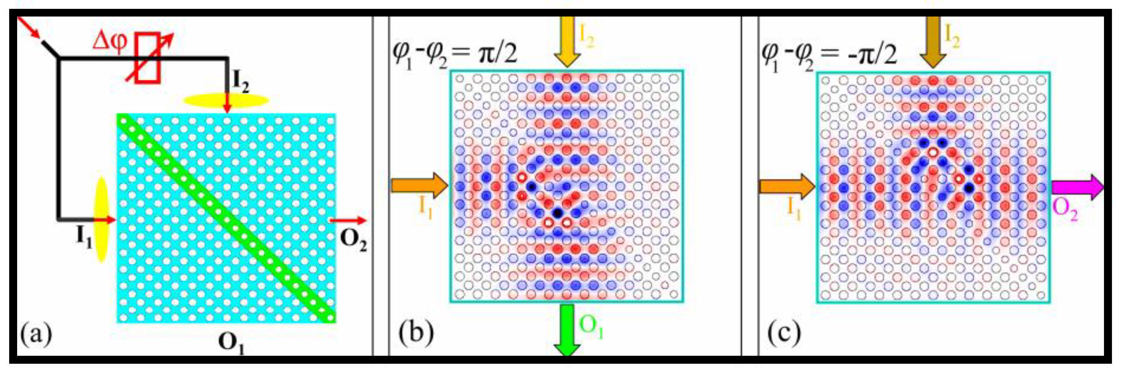
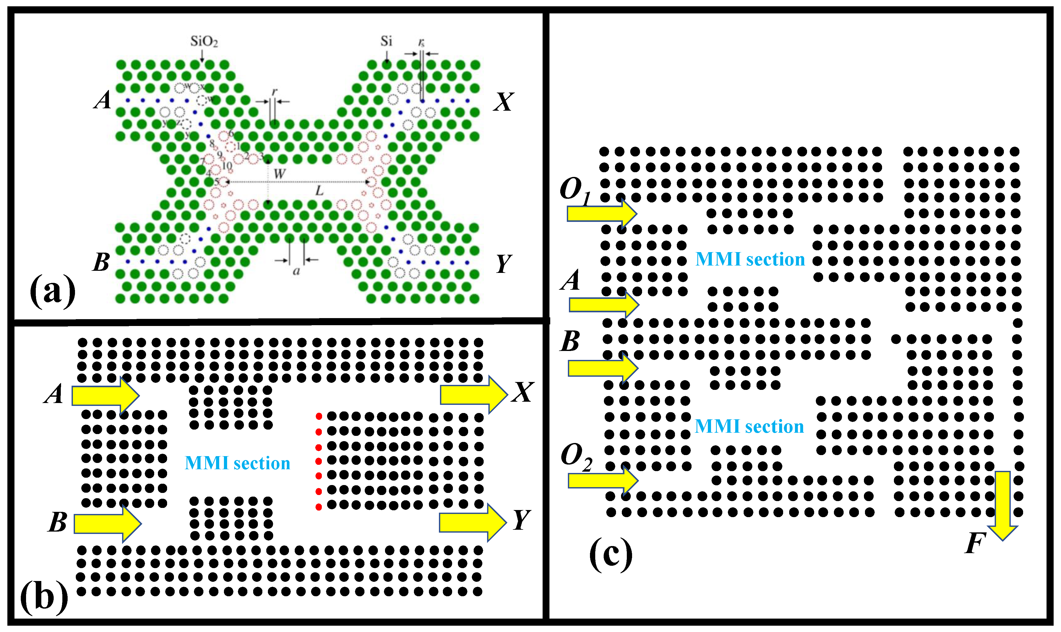
5. Photonic Crystal (PhC) All-Optical Logic Gates (OLGs)

With the progress of science, there seems to be a significant change in computing in many ways over the years. Mechanical methods were used to create the earliest computers (1623 to 1945) [104]. Researchers attempted to create apparatuses that could readily answer mathematical problems in the early seventeenth century. Several scientists, including Gottfried Leibnitz, Wilhelm Schickhard, and Blaire Pascal, attempted to develop a calculator that could handle addition, subtraction, multiplication, and division. George Schertz and Edward Schertz created a system that could handle 15-digit numbers using a 4-bit difference engine. One of the institutions that employed the mechanical computer for punch card technology for the enumeration was the United States Census Bureau, which was designed by Herman Hollerith of the International Business Machines [104].
A wide range of components, including optical gates, optical switches, optical interconnects, and optical memory, are required to form an optical computer. Because of its applicability in ultrafast information processing [105] and the ways to carry out various logical operations in OC systems, all-optical LGs have become popular recently [106]. As a result, building all-optical LGs is the first step in achieving advanced digital functionality in optical computers. Electronic LGs were previously employed, but the highest switching speed obtained was 50 ps with an average power of 0.5 mW per switching [107]. The reduced capacitance of p-n junctions in semiconductor-based LGs is the explanation for this.
Despite today’s electronic LGs being tiny, switching is still restricted by interlinking capacitance; on the other side, optical LGs have switching speeds in the femtosecond range and are only restricted by the speed of light traveling through them [108]. The prototype of all-optical LGs can be made by a variety of methods. The first technique employs a semiconductor optical amplifier (SOA), which has a high gain owing to refractive index variations. The original way to make all-optical LGs was to use one of three approaches to introduce nonlinearity: cross-gain modulation [109][110], cross-phase modulation [109], or four-wave mixing [110][111]. SOA was also utilized to construct SOA-assisted interferometer-based gates, which are all-optical LGs [112]. However, SOA-based gates have several drawbacks, including SOA-based apparatuses being constrained by SOA’s slow carrier recovery time, unsteady gates owing to polarization sensitivity, and the SOA Mach–Zehnder interferometer (MZI) technique, which necessitates more than two SOAs and complicates the scheme by needing the proper tuning of the filter for SOA with the help of fiber LGs, as detuning of the filter. Nonlinear WGs, in which localized nonlinear media have been used by adjusting the control power, are another way of developing all-optical LGs [113][114][115]. Nonlinear WG-based gates have several drawbacks, including a substantial I/P signal power need and polarization dependency, which pose production issues.
PhCs are periodic structured dielectric or EM media with photonic bandgaps (PBGs) that prevent light from propagating through them [116][117][118][119]. John was the one who introduced PhC [120]. Unlike semiconductor crystals, which alter the characteristics of electrons, these crystals impact the characteristics of photons. Light has various benefits over electrons, including the ability to move faster in dielectric material than electrons in the conductive metal and a larger data capacity in the dielectric than electrons. One of the most significant functions in the realm of high data transmission that 2D PhCs may achieve is all-optical LGs. Furthermore, there are two main types of PhC-based gates: PBG-based gates and non-PBG-based LGs.
(a)
Non-PBG-based all-OLGs
Instead of establishing the PBG of the apparatuses, the I/P beam of any wavelength is injected at the I/P, and a logic function is conducted utilizing a self-collimated beam (SCB) in non-PBG-based PhC gates. In this case, incoming light transmits to a device in a given direction without diffraction. The phenomena of total internal reflection are utilized to construct all-optical LGs utilizing an SCB. Total internal reflection refers to the angle of incidence being larger than the critical angle, according to the relation ϴ > arc sin(nL/nH), where nL represents the low refractive index and nH represents the high refractive index. In a 2D PhC, a device for the photonic-integrated circuit (PIC) was formulated and established on an SCB [121]. The structure is useful for making optical switches and LGs, both of which are important parts of a PIC. The device with Si rods in the air was designed using square lattice geometry. To achieve the outphasing at the O/P, a low refractive index medium was created such that one-half of the beam was allowed to propagate while the other was reflected, suggesting the existence of transmitted and reflected beams for the I/P signals. By altering the phase difference between the reflected and transmitted beams, the OR and XOR gate structures were developed. When the phase difference between the I/P beams was 2kπ + π/2, O/P O1 functioned as an OR gate and O/P O2 functioned as an XOR gate, as illustrated in Figure 5a–c [122]. O1 worked as an XOR gate and O2 acted as an OR gate when the phase difference was 2kπ–π/2 owing to a phase difference of –π/2 between the I/P beams. The device’s frequency range was 0.188 to 0.199, with a 17 dB extinction ratio.
Figure 5. (a). The switch’s schematic representation. On the I/P faces I1 and I2, two beams with different phases collide. The computed steady-state field pattern of the E-polarized mode at 0.194 (a/λ) when incoming beams propagate in the Г-M direction in (b,c). The phase difference between the two incident beams is adjusted to π/2 and −π/2, respectively, by the phase difference φ1 − φ2 [121].
For the PIC implementation, an all-OLG architecture of NOT, OR, AND, and XOR gates centered on the SCB was presented [122]. The structure was constructed using 2D square lattice geometry with air holes in Si as the foundation material. The framework has been developed and established on the phase difference between the I/P signals, following the phenomena of the SCB. When light is launched at both the I/P as well as reference points of the same intensities, there was partial reflectance of the I/P light wave while the reference light wave was completely mirrored, and when these light waves interfered with each other, there was an O/P that relied on the phases at the I/Ps and interfered in a constructive manner or destructively. It was proposed to use SCB-based logic gates for AND, NAND, XNOR, and NOR OLGs. The framework has been developed with triangular lattice topology and rods made of Si material in an air background [123]
(b)
PBG-based all-OLGs
The PBG of the architecture is utilized to detect hidden frequency ranges that cannot flow through the structure in PBG-based all-optical OLGs. By adding various forms of defects, one of the suppressed frequencies can transmit across the structure. MMI, nonlinear Kerr effect, and interference are commonly used in the design of PBG-based OLGs. In [124], MMI-based AND and XOR OLGs are introduced, as depicted in Figure 6a, with A and B I/P points and X and Y O/P points. It was constructed utilizing triangular lattice geometry, SiO2 as the foundation material, and Si rods. An I/P signal with an outphasing of π was transmitted at point A. On point B, the signal was emitted with an outphasing of –π/2, which represented logic “1” and creates logic “1” at the O/P point. When there was a phase of π at point A, which indicated logic “0”, and another signal with outphasing π/2 at point B, which expressed logic “0”, the O/P generated logic “1”. In another scenario, when a signal with an outphasing of π expressed logic “0” at I/P point A while a signal with an outphasing of π/2 stated logic “0” at point B, logic “0” was identified at the O/P. When both I/Ps at point A and point B displayed logic “1” with outphasings of 0 and −π/2, the O/P point sensed logic “0”. The AND OLG was constructed using the same concept by modifying the length of MMI and appropriately choosing I/P signal phases. Both AND and XOR OLGs obtained a CR of roughly 6.79 dB.
Figure 6. Schematic of OLGs established on MMI. Inspired by [125], (a) AND/XOR OLG, (b) XOR/XNOR, (c) AND and NOR OLGs. Inspired by [126].
The self-imaging mechanism underpins the operation of MMI apparatuses. The tiny field at the I/P activates guided modes in the effective region, which constitutes interference in that region, in this phenomenon. Binary phase-shift keyed (BPSK) signals are utilized as I/P logic values because, in MMI, I/P values are often expressed by the phase of the I/P signals, and O/P logic levels are expressed using amplitude independent of phase. Silicon material was employed for the rods in the suggested device, with air as the background oriented in a square lattice shape [126]. As indicated in Figure 6b, A and B are the I/P points of the XOR/XNOR OLG arrangement, whereas X and Y are the O/P points. When there is an outphasing of π at point A, logic “0” was stated as signal I/P, while logic “1” is explicit with phase 0. When there was an outphasing of 3π/2 at point B, logic “0” was expressed as signal I/P, while logic “1” was explicit with phase 0. To realize the AND OLG indicated in Figure 6c, I/Ps A and B with phase π represented logic “0,” whereas I/Ps A and B with phase 0 represented logic “1”. With an outphasing of 3π/2, logic “0” was established at O1 and O2. The sole change in designing the NOR OLG was that O1 and O2 were locked at logic “1”, which was represented by an outphasing of π/2. The AND OLG realized a CR of 21 dB, whereas the NOR operation achieved a CR of 19 dB [126]

6. Resonant Nanophotonic Constructions

Nanophotonic components are being suggested as a novel foundation for analog optoelectronic computing [135][136][137][138]. It was shown that a layer of a well-designed metamaterial can visually execute several essential mathematical operations (differentiation and integration of light waves concerning a spatial coordinate, convolution of light waves with a predefined core) [136]. It generated a lot of interest and aided the creation of novel nanophotonic structures for AOC. Differentiation (integration) of the pulse envelope is commonly understood in the context of temporal differentiation (integration) of a light wave (optical pulse). The most important findings in fiber optic network design and production for the differentiation (integration) of optical pulses propagating in OFs were acquired [139][140][141][142][143][144][145]. Bragg resonant structures and RRs have been proposed to perform time-domain differentiation (integration) procedures. Because the spectra of reflection and transmission in the proximity of resonances are characterized by the Fano profile, and in a certain frequency, intervals may accurately estimate the transfer functions of differentiating and integrating filters, resonant formations can be used to implement differentiation and integration operations. It is worth noting that more complex systems with many resonators may solve ordinary differential equations of various orders as well as solutions of differential equations in the temporal domain [146][147][148][149].
The employment of differentiation and integration of light pulses traveling in free space is also of importance, in addition to the temporal changes of light signals traveling through OFs. Soifer et al. achieved several significant discoveries in this field. The processes of differentiation (integration) of the pulse envelope may be successfully conducted by employing a resonant diffraction grating, as described in studies [150][151][152][153][154][155]. High-order derivatives may be calculated quickly using a set of multiple stacked diffraction gratings [154]. The creation of the theory of spatiotemporal transformations of light waves was established on the theoretical explanation of diffraction of light pulses on resonant diffractive assemblies.
An optical correlator can conduct a wide range of spatial filtering functions on light waves. The optical correlator, also known as the coherent optical Fourier processor, is made up of two lenses that execute the FT optically and a spatial filter that encapsulates the transmission function characterizing the incoming light beam’s needed spatial transformation. As a spatial filter, a differentiating filter with a complicated transmission function corresponding to the spatial frequency should be utilized to accomplish the differentiation operation in such a scheme. Nevertheless, the optical correlator’s significantly larger size limits its practical applicability. Using nanophotonic configurations, spatial differentiators and integrators with a thickness similar to the wavelength of the modulated light wave may be created. In 2014, the idea of implementing spatial changes of light waves utilizing nanophotonic apparatuses was introduced. The fundamental work in [135] was a theoretical investigation of the execution of spatial differentiation, integration, and convolution operations on light waves. There were two ways offered. The first was to employ tiny analogues of optical correlators, with the traditional Fourier lenses being substituted by tiny layers with a gradient refractive index and an MS serving as the spatial filter storing the requisite transmission function. The second method was to utilize a multilayer structure that was particularly built to accomplish the spatial transformation of the I/P signal indicated by the convolution operator with a certain core.
Bozhevolnyi et al. conducted the first study proving the capability of differentiation and integration regarding a spatial factor using an MS in 2015 [138]. The first strategy was utilized for optical differentiation and integration, in which the processes were carried out in an optical correlator comprised of a lens and a reflecting spatial filter. A reflecting MS encrypting transmission function of a differentiating (integrating) filter was employed as the filter. The MS in question was made up of a series of the metal–insulator–metal resonant circuit [156][157]. Fabry–Perot resonances of plasmonic modes traveling in metal slots are supported by such resonators. The experimental findings provided in [138] show that optical differentiation (integration) may be implemented with the use of an MS. Simultaneously, it should be highlighted that the MSs in [138] only conduct differentiation and integration tasks in conjunction with a lens, preventing the suggested system from being compact. In subsequent work [158][159][160], dielectric MSs were used to encode the essential transmission functions of the spatial filter, causing a reduction in losses due to absorption in the metal claddings of nano-resonators and enhanced performance in the deployment of differential and integral conversions.
Because the nanophotonic assembly directly executes the needed spatial change of the I/P signal, the second option is more plausible. In this example, the optical correlator is replaced with a single assembly (with no extra lenses). It is worth noting that the structure’s reflection and transmission coefficients as functions of spatial frequency (a tangential component of the incoming wave vector) match the transfer functions defining the incident light beam’s conversion [138]. As a result, nanophotonic assemblies with reflection (or transmission) coefficients that approximate the transfer functions of the differentiator or integrator would be required to accomplish the elementary actions of spatial differentiation or integration of the light beam. A resonant reflection or transmission band with a Lorentzian line form can be used to mimic the integrator’s transfer function. About the zeros of reflection and transmission happening near the resonance, the differentiator’s transfer function is very well modeled.
Soifer et al. achieved the most important results in this sector. The work of this group initially established that phase-shifted Bragg gratings (PSBGs) [161][162][163], resonant diffraction gratings [164][165], PhC resonators [166][167][168][169][170][171], and three-layer arrangements with W-shaped refractive index profiles may efficiently execute the functions of differentiation and integration of the light wave profile [172]. It is worth noting that resonant nanostructures can also be used to compute the Laplace operator optically [163]. In image processing, this method is utilized to recognize edges. The first investigation affirming the potential of differentiating a spatial variable using the resonant diffraction grating was carried out in 2018 using the apparatuses of the Collective Use Center “Nano-Photonics and Diffraction Optics” [173], which was established by a cooperative endeavor of Samara University and the Russian Academy of Sciences’ Image Processing Systems Institute [172]. It resulted in a high level of distinction that was far superior to the quality of differentiation attained using MSs [138]. It is also important to note that differentiators and integrators founded on resonant diffraction gratings and PSBGs are not only smaller but also easier to fabricate than equivalent apparatuses that rely on correlators with MSs. The emphasis of [174] is a differentiator comprising of a prism with a metal film placed on one of its sides; specifically, the differentiator is composed of a prism with a metal film coated on one of its sides [175][176]. The incident light wave’s differentiation is carried out in this scenario in reflection due to the incident light wave’s activation of a surface plasmon-polariton on the metal film’s surface. The effectiveness of employing such a framework for optical edge detection was proved in experiments.
The first-order differentiation of the transverse profile of an incoming light wave regarding a spatial variable is demonstrated experimentally using a subwavelength diffraction grating, as shown in Figure 7a [165]Figure 7b shows a typical SEM picture of the manufactured grating. The experimental findings accord well with the provided theoretical model, implying that the differentiation occurs in transmission at oblique incidence and is linked to the grating’s guided-mode resonance. As per this concept, the grating’s transfer function about the resonance is similar to that of an exact differentiator. Figure 7c,d illustrates the incident Gaussian light wave and transmitted light wave profiles, respectively. The incident light wave has a Gaussian shape to it. The precise derivative agrees well with the form of the transmitted light wave (Figure 7e). The profile of the transmitted light wave estimated considering manufactured structural flaws is also shown in Figure 7f. The configuration under consideration might be used in the development of novel photonic apparatuses for light wave shaping, optical data processing, and AOC.
Figure 7. (a) The diffraction of an optical light wave on a resonant diffraction assembly made up of a grating on top of a slab waveguide layer put on a substrate [165], (b) The diffraction grating was created using ERP-40 electron resist on top of a TiO2 layer, as shown by SEM [165], (c) Measured profile of incident Gaussian light wave [165], (d) Measured profile of transmitted light wave [165], (e) Analytically derived derivative of incident light wave [165], (f) Profile of transmitted light wave estimated taking into account manufactured structural flaws [165].

This entry is adapted from the peer-reviewed paper 10.3390/nano12132171

References

  1. Goodman, J. Introduction to Fourier Optics; McGraw-Hill: San Francisco, CA, USA, 1968.
  2. Carpenter, J. Holographic Mode Division Multiplexing in Optical Fibres; University of Cambridge: Cambridge, UK, 2012.
  3. Stroke, G.W. An Introduction to Coherent Optics and Holography; Academic Press: New York, NY, USA, 1966.
  4. Preston, K., Jr. Coherent Optical Computers; McGraw-Hill: New York, NY, USA, 1972.
  5. Lugt, A. Coherent optical processing. Proc. IEEE 1974, 62, 1300–1319.
  6. Perrin, M.; Metzger, G. Principles and feasibility of an optical preprocessor in high-energy physics. Nucl. Instrum. Methods 1975, 126, 509–518.
  7. Kotlyar, V.V.; Khonina, S.N.; Soĭfer, V.A. Light field decomposition in angular harmonics by means of diffractive optics. J. Mod. Opt. 1998, 45, 1495–1506.
  8. Khonina, S.N.; Kotlyar, V.V.; Soifer, V.A.; Paakkonen, P.; Turunen, J. Measuring the light field orbital angular momentum using DOE. Opt. Mem. Neural Netw. 2001, 10, 241–255.
  9. Kotlyar, V.V.; Khonina, S.N.; Soifer, V.A.; Wang, Y. Light field orbital angular moment measurement with the help of diffractive optical element. Avtometriya 2002, 38, 33–44.
  10. Kotlyar, V.V.; Kovalev, A.A.; Volyar, A.V. Topological charge of optical vortices and their superpositions. Comput. Opt. 2020, 44, 145–154.
  11. Reddy, A.N.K.; Anand, V.; Khonina, S.N.; Podlipnov, V.V.; Juodkazis, S. Robust Demultiplexing of Distinct Orbital Angular Momentum Infrared Vortex Beams Into Different Spatial Geometry Over a Broad Spectral Range. IEEE Access 2021, 9, 143341–143348.
  12. Porfirev, A.P.; Khonina, S.N. Experimental investigation of multi-order diffractive optical elements matched with two types of Zernike functions. Proc. SPIE 2016, 9807, 98070E.
  13. Degtyarev, S.A.; Porfirev, A.P.; Khonina, S.N. Zernike basis-matched multi-order diffractive optical elements for wavefront weak aberrations analysis. Proc. SPIE 2017, 10337, 103370Q.
  14. Khorin, P.A.; Volotovskiy, S.G.; Khonina, S.N. Optical detection of values of separate aberrations using a multi-channel filter matched with phase Zernike functions. Comput. Opt. 2021, 45, 525–533.
  15. Khonina, S.N.; Karpeev, S.V.; Porfirev, A.P. Wavefront Aberration Sensor Based on a Multichannel Diffractive Optical Element. Sensors 2020, 20, 3850.
  16. Khorin, P.A.; Porfirev, A.P.; Khonina, S.N. Adaptive Detection of Wave Aberrations Based on the Multichannel Filter. Photonics 2022, 9, 204.
  17. Soifer, V.A.; Golub, M.A.; Khonina, S.N. Decorrelated features of images extracted with the aid of optical Karhunen-Loeve expansion. Pattern Recognit. Image Anal. 1993, 3, 289–295.
  18. Soifer, V.A.; Khonina, S.N. Stability of the Karhunen-Loeve expansion in the problem of pattern recognition. Pattern Recognit. Image Anal. 1994, 4, 137–148.
  19. Soifer, V.A.; Kotlyar, V.V.; Khonina, S.N. An optical method of directions field construction. Avtometriya 1996, 1, 31–36.
  20. Soifer, V.A.; Kotlyar, V.V.; Khonina, S.N.; Skidanov, R.V. Optical methods of fingerprints identification. Comput. Opt. 1996, 16, 78–89.
  21. Soifer, V.; Kotlyar, V.; Khonina, S.; Skidanov, R. Optical–digital methods of fingerprint identification. Opt. Lasers Eng. 1998, 29, 351–359.
  22. Khonina, S.; Kotlyar, V.V.; Skidanov, R.V.; Soifer, V.; Soĭfer, V.A. Optodigital system for identifying fingerprints in real time. J. Opt. Technol. 2003, 70, 586–589.
  23. Khonina, S.N.; Demidov, A.S. Extended depth of focus through imaging system’s phase apodization in coherent and incoherent cases. Opt. Mem. Neural Netw. 2014, 23, 130–139.
  24. Khonina, S.N.; Ustinov, A.V. Generalized apodization of an incoherent imaging system aimed for extending the depth of focus. Pattern Recognit. Image Anal. 2015, 25, 626–631.
  25. Khonina, S.N.; Ustinov, A.V.; Porfirev, A.P. Dynamic focal shift and extending depth of focus based on the masking of the illuminating beam and using an adjustable axicon. J. Opt. Soc. Am. A 2019, 36, 1039–1047.
  26. Khonina, S.; Volotovskiy, S.; Dzyuba, A.; Serafimovich, P.; Popov, S.; Butt, M. Power Phase Apodization Study on Compensation Defocusing and Chromatic Aberration in the Imaging System. Electronics 2021, 10, 1327.
  27. Khonina, S.N.; Kotlyar, V.V.; Shinkaryev, M.V.; Soi-Fer, V.A.; Uspleniev, G.V. The Phase Rotor Filter. J. Mod. Opt. 1992, 39, 1147–1154.
  28. Ananin, M.A.; Khonina, S.N. Modelling of optical processing of images with use of the vortical spatial filter. Comput. Opt. 2009, 33, 466–472.
  29. Davis, J.A.; McNamara, D.E.; Cottrell, D.M.; Campos, J. Image processing with the radial Hilbert transform: Theory and experiments. Opt. Lett. 2000, 25, 99–101.
  30. Guo, C.-S.; Han, Y.-J.; Xu, J.-B.; Ding, J. Radial Hilbert transform with Laguerre-Gaussian spatial filters. Opt. Lett. 2006, 31, 1394–1396.
  31. Lazarev, G.; Hermerschmidt, A. LCOS Spatial Light Modulators: Trends and Applications. In Optical Imaging and Metrology: Advanced Technologies; Osten, W., Reingand, N., Eds.; Wiley-VCH: Weinheim, Germany, 2012; pp. 1–29.
  32. Pivnenko, M.; Li, K.; Chu, D. Sub-millisecond switching of multi-level liquid crystal on silicon spatial light modulators for increased information bandwidth. Opt. Express 2021, 29, 24614–24628.
  33. Jin, D.; Zhou, R.; Yaqoob, Z.; So, P.T.C. Dynamic spatial filtering using a digital micromirror device for high-speed optical diffraction tomography. Opt. Express 2018, 26, 428–437.
  34. Turtaev, S.; Leite, I.T.; Mitchell, K.J.; Padgett, M.J.; Phillips, D.B.; Cizmar, T. Comparison of nematic liquid-crystal and DMD based spatial light modulation in complex photonics. Opt. Express 2017, 25, 29874–29884.
  35. Phase Spatial Light Modulator LCOS-SLM. Available online: https://www.hamamatsu.com/eu/en/product/optical-components/lcos-slm.html (accessed on 23 June 2022).
  36. Kovachev, M.; Ilieva, R.; Onural, L.; Esmer, G.B.; Reyhan, T.; Benzie, P.; Watson, J.; Mitev, E. Reconstruction of Computer Generated Holograms by Spatial Light Modulators. In Multimedia Content Representation, Classification and Security; Gunsel, B., Jain, A.K., Tekalp, A.M., Sankur, B., Eds.; Springer: Berlin/Heidelberg, Germany, 2006; pp. 706–713.
  37. Younus, S.H.; Hussein, A.T.; Alresheedi, M.T.; Elmirghani, J. CGH for Indoor Visible Light Communication System. IEEE Access 2017, 5, 24988–25004.
  38. Torii, Y.; Balladares-Ocaña, L.; Martinez-Castro, J. An Iterative Fourier Transform Algorithm for digital hologram generation using phase-only information and its implementation in a fixed-point digital signal processor. Optik 2013, 124, 5416–5421.
  39. Kettunen, V.; Ripoll, O.; Herzig, H.P. Review of iterative Fourier-transform algorithms for beam shaping applications. Opt. Eng. 2004, 43, 2549–2556.
  40. Roelens, M.A.F.; Frisken, S.; Bolger, J.A.; Abakoumov, D.; Baxter, G.; Poole, S.; Eggleton, B.J. Dispersion Trimming in a Reconfigurable Wavelength Selective Switch. J. Light. Technol. 2008, 26, 73–78.
  41. Wang, M.; Zong, L.; Mao, L.; Marquez, A.; Ye, Y.; Zhao, H.; Caballero, F.J.V. LCoS SLM Study and Its Application in Wavelength Selective Switch. Photonics 2017, 4, 22.
  42. Turunen, J.; Wyrowski, F. Diffractive Optics for Industrial and Commercial Applications; John Wiley and Sons: Hoboken, NJ, USA, 1997.
  43. Osten, W.; Kohler, C.; Liesener, J. Evaluation and Application of Spatial Light Modulators for Optical Metrology. Opt. Pura Apl. 2005, 38, 71–81.
  44. Varga, J.J.M.; A Solís-Prosser, A.M.; Rebón, L.; Arias, A.; Neves, L.; Iemmi, C.; Ledesma, S. Preparing arbitrary pure states of spatial qudits with a single phase-only spatial light modulator. J. Phys. Conf. Ser. 2015, 605, 012035.
  45. Schröder, J.; Roelens, M.; Du, L.; Lowery, A.; Eggleton, B. LCOS based waveshaper technology for optical signal processing and performance monitoring. In Proceedings of the 17th Opto-Electronics and Communications Conference, Busan, Korea, 2–6 July 2012; pp. 859–860.
  46. Barbier, P.; Moddel, G. Spatial light modulators: Processing light in real time. Opt. Photon. News 1997, 8, 17–21.
  47. Shrestha, P.K.; Chun, Y.T.; Chu, D. A high-resolution optically addressed spatial light modulator based on ZnO nanoparticles. Light. Sci. Appl. 2015, 4, e259.
  48. Chen, P.; Ma, L.-L.; Hu, W.; Shen, Z.-X.; Bisoyi, H.K.; Wu, S.-B.; Ge, S.-J.; Li, Q.; Lu, Y.-Q. Chirality invertible superstructure mediated active planar optics. Nat. Commun. 2019, 10, 2518.
  49. Smith, D. Lasers, nonlinear optics and optical computers. Nature 1985, 316, 319–324.
  50. Shih, M.Y.; Shishido, A.; Khoo, I.C. All-optical image processing by means of a photosensitive nonlinear liquid-crystal film: Edge enhancement and image addition–subtraction. Opt. Lett. 2001, 26, 1140–1142.
  51. Zhang, J.; Wang, H.; Yoshikado, S.; Aruga, T. Incoherent-to-coherent conversion by use of the photorefractive fanning effect. Opt. Lett. 1997, 22, 1612–1614.
  52. Woods, D.; Naughton, T.J. Photonic neural networks. Nat. Phys. 2012, 8, 257–259.
  53. Solodar, A.; Kumar, T.A.; Sarusi, G.; Abdulhalim, I. Infrared to visible image up-conversion using optically addressed spatial light modulator utilizing liquid crystal and InGaAs photodiodes. Appl. Phys. Lett. 2016, 108, 021103.
  54. Kirzhner, M.G.; Klebanov, M.; Lyubin, V.; Collings, N.; Abdulhalim, I. Liquid crystal high-resolution optically addressed spatial light modulator using a nanodimensional chalcogenide photosensor. Opt. Lett. 2014, 39, 2048–2051.
  55. Li, S.-Q.; Xu, X.; Veetil, R.M.; Valuckas, V.; Paniagua-Domínguez, R.; Kuznetsov, A.I. Phase-only transmissive spatial light modulator based on tunable dielectric metasurface. Science 2019, 364, 1087–1090.
  56. Li, J.; Yu, P.; Zhang, S.; Liu, N. Electrically-controlled digital metasurface device for light projection displays. Nat. Commun. 2020, 11, 3574.
  57. Park, J.; Gil Jeong, B.; Kim, S.I.; Lee, D.; Kim, J.; Shin, C.; Lee, C.B.; Otsuka, T.; Kyoung, J.; Kim, S.; et al. All-solid-state spatial light modulator with independent phase and amplitude control for three-dimensional LiDAR applications. Nat. Nanotechnol. 2020, 16, 69–76.
  58. Gong, S.; Ren, M.; Wu, W.; Cai, W.; Xu, J. Optically addressed spatial light modulator based on nonlinear metasurface. Photon. Res. 2021, 9, 610.
  59. Heck, M. Optical Computers Light Up the Horizon. 2018. Available online: https://phys.org/news/2018-03-optical-horizon.html (accessed on 28 April 2022).
  60. Waldrop, M. The chips are down for Moore’s law. Nat. News 2016, 530, 144.
  61. Atabaki, A.H.; Moazeni, S.; Pavanello, F.; Gevorgyan, H.; Notaros, J.; Alloatti, L.; Wade, M.T.; Sun, C.; Kruger, S.A.; Meng, H.; et al. Integrating photonics with silicon nanoelectronics for the next generation of systems on a chip. Nature 2018, 556, 349–354.
  62. Paniccia, M. A perfect marriage: Optics and silicon: Integrated silicon-based photonics now running at 50 Ggps, with Terabit speeds on the horizon. Optik. Photon. 2011, 6, 34–38.
  63. Liu, K.; Ye, C.R.; Khan, S.; Sorger, V.J. Review and perspective on ultrafast wavelength-size electro-optic modulators. Laser Photon. Rev. 2015, 9, 172–194.
  64. Chung, S.; Nakai, M.; Hashemi, H. Low-power thermo-optic silicon modulator for large-scale photonic integrated systems. Opt. Express 2019, 27, 13430–13459.
  65. Lee, B.; Biberman, A.; Chan, J.; Bergman, K. High-Performance Modulators and Switches for Silicon Photonic Networks-on-Chip. IEEE J. Sel. Top. Quantum Electron. 2009, 16, 6–22.
  66. Ying, Z.; Feng, C.; Zhao, Z.; Soref, R.; Pan, D.; Chen, R.T. Integrated multi-operand electro-optic logic gates for optical computing. Appl. Phys. Lett. 2019, 115, 171104.
  67. Xiao, X.; Xu, H.; Li, X.; Li, Z.; Chu, T.; Yu, Y.; Yu, J. High-speed, low-loss silicon Mach–Zehnder modulators with doping optimization. Opt. Express 2013, 21, 4116–4125.
  68. Shu, H.-W.; Jin, M.; Tao, Y.-S.; Wang, X.-J. Graphene-based silicon modulators. Front. Inf. Technol. Electron. Eng. 2019, 20, 458–471.
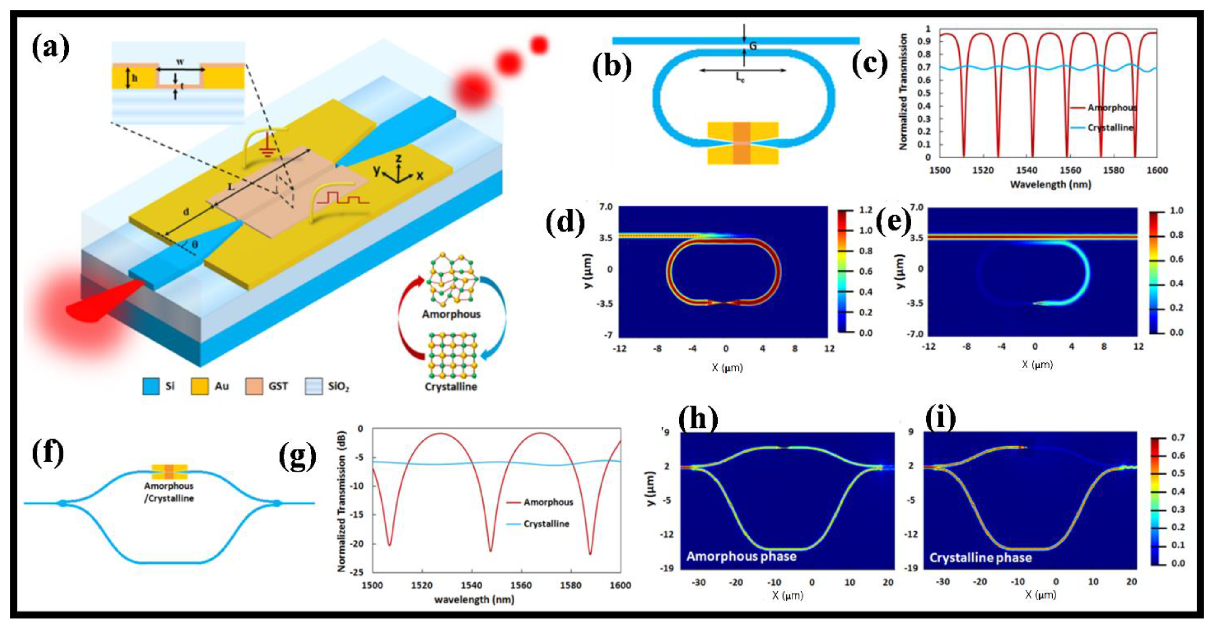
  69. Zhang, Q.; Zhang, Y.; Li, J.; Soref, R.; Gu, T.; Hu, J. Broadband nonvolatile photonic switching based on optical phase change materials: Beyond the classical figure-of-merit. Opt. Lett. 2017, 43, 94–97.
  70. Yang, Z.; Ramanathan, S. Breakthroughs in Photonics 2014: Phase Change Materials for Photonics. IEEE Photon. J. 2015, 7, 1–5.
  71. Badri, S.H.; Farkoush, S.G. Subwavelength grating waveguide filter based on cladding modulation with a phase-change material grating. Appl. Opt. 2021, 60, 2803–2810.
  72. Wang, J.; Wang, L.; Liu, J. Overview of Phase-Change Materials Based Photonic Devices. IEEE Access 2020, 8, 121211–121245.
  73. Badri, S.H.; Gilarlue, M.M.; Farkoush, S.G.; Rhee, S.-B. Reconfigurable bandpass optical filters based on subwavelength grating waveguides with a Ge2Sb2 Te5 cavity. J. Opt. Soc. Am. B 2021, 38, 1283–1289.
  74. Ghosh, R.; Dhawan, A. Integrated non-volatile plasmonic switches based on phase-change-materials and their application to plasmonic logic circuits. Sci. Rep. 2021, 11, 18811.
  75. Prieto, A.; Prieto, B.; Ortigosa, E.M.; Ros, E.; Pelayo, F.; Ortega, J.; Rojas, I. Neural networks: An overview of early research, current frameworks and new challenges. Neurocomputing 2016, 214, 242–268.
  76. LeCun, Y.; Bengio, Y.; Hinton, G. Deep learning. Nature 2015, 521, 436–444.
  77. Krizhevsky, A.; Sutskever, I.; Hinton, G.E. Imagenet classification with deep convolutional neural networks. NIPS 2012, 60, 84–90.
  78. Nitta, T. Orthogonality of Decision Boundaries in Complex-Valued Neural Networks. Neural Comput. 2004, 16, 73–97.
  79. Aizenberg, I. Complex-Valued Neural Networks with Multi-Valued Neurons; Springer: Berlin/Heidelberg, Germany, 2011.
  80. Peng, H.-T.; Nahmias, M.A.; De Lima, T.F.; Tait, A.N.; Shastri, B.J. Neuromorphic Photonic Integrated Circuits. IEEE J. Sel. Top. Quantum Electron. 2018, 24, 1–15.
  81. Sze, V.; Chen, Y.-H.; Yang, T.-J.; Emer, J.S. Efficient Processing of Deep Neural Networks: A Tutorial and Survey. Proc. IEEE 2017, 105, 2295–2329.
  82. de Lima, T.F.; Peng, H.-T.; Tait, A.N.; Nahmias, M.A.; Miller, H.B.; Shastri, B.J.; Prucnal, P.R. Machine Learning With Neuromorphic Photonics. J. Light. Technol. 2019, 37, 1515–1534.
  83. Lin, X.; Rivenson, Y.; Yardimci, N.T.; Veli, M.; Luo, Y.; Jarrahi, M.; Ozcan, A. All-optical machine learning using diffractive deep neural networks. Science 2018, 361, 1004–1008.
  84. Vandoorne, K.; Mechet, P.; Van Vaerenbergh, T.; Fiers, M.; Morthier, G.; Verstraeten, D.; Schrauwen, B.; Dambre, J.; Bienstman, P. Experimental demonstration of reservoir computing on a silicon photonics chip. Nat. Commun. 2014, 5, 3541.
  85. Harris, N.C.; Carolan, J.; Bunandar, D.; Prabhu, M.; Hochberg, M.; Baehr-Jones, T.; Fanto, M.L.; Smith, A.M.; Tison, C.C.; Alsing, P.M.; et al. Linear programmable nanophotonic processors. Optica 2018, 5, 1623–1631.
  86. Williamson, I.A.D.; Hughes, T.W.; Minkov, M.; Bartlett, B.; Pai, S.; Fan, S. Reprogrammable Electro-Optic Nonlinear Activation Functions for Optical Neural Networks. IEEE J. Sel. Top. Quantum Electron. 2019, 26, 1–12.
  87. Bueno, J.; Maktoobi, S.; Froehly, L.; Fischer, I.; Jacquot, M.; Larger, L.; Brunner, D. Reinforcement learning in a large-scale photonic recurrent neural network. Optica 2018, 5, 756–760.
  88. Ambrogio, S.; Narayanan, P.; Tsai, H.; Shelby, R.M.; Boybat, I.; Di Nolfo, C.; Sidler, S.; Giordano, M.; Bodini, M.; Farinha, N.C.P.; et al. Equivalent-accuracy accelerated neural-network training using analogue memory. Nature 2018, 558, 60–67.
  89. Li, C.; Belkin, D.; Li, Y.; Yan, P.; Hu, M.; Ge, N.; Jiang, H.; Montgomery, E.; Lin, P.; Wang, Z.; et al. Efficient and self-adaptive in-situ learning in multilayer memristor neural networks. Nat. Commun. 2018, 9, 2385.
  90. Yao, P.; Wu, H.; Gao, B.; Tang, J.; Zhang, Q.; Zhang, W.; Yang, J.J.; Qian, H. Fully hardware-implemented memristor convolutional neural network. Nature 2020, 577, 641–646.
  91. Rakkiyappan, R.; Velmurugan, G.; Li, X. Complete Stability Analysis of Complex-Valued Neural Networks with Time Delays and Impulses. Neural Process. Lett. 2014, 41, 435–468.
  92. Wang, H.; Duan, S.; Huang, T.; Wang, L.; Li, C. Exponential Stability of Complex-Valued Memristive Recurrent Neural Networks. IEEE Trans. Neural Netw. Learn. Syst. 2016, 28, 766–771.
  93. Velmurugan, G.; Rakkiyappan, R.; Vembarasan, V.; Cao, J.; Alsaedi, A. Dissipativity and stability analysis of fractional-order complex-valued neural networks with time delay. Neural Netw. 2016, 86, 42–53.
  94. Hirose, A. Applications of complex-valued neural networks to coherent optical computing using phase-sensitive detection scheme. Inf. Sci. Appl. 1994, 2, 103–117.
  95. Zhang, H.; Gu, M.; Jiang, X.D.; Thompson, J.; Cai, H.; Paesani, S.; Santagati, R.; Laing, A.; Zhang, Y.; Yung, M.H.; et al. An optical neural chip for implementing complex-valued neural network. Nat. Commun. 2021, 12, 457.
  96. Wei, H.; Wang, Z.; Tian, X.; Käll, M.; Xu, H. Cascaded logic gates in nanophotonic plasmon networks. Nat. Commun. 2011, 2, 387.
  97. Wei, H.; Li, Z.; Tian, X.; Wang, Z.; Cong, F.; Liu, N.; Zhang, S.; Nordlander, P.; Halas, N.J.; Xu, H. Quantum Dot-Based Local Field Imaging Reveals Plasmon-Based Interferometric Logic in Silver Nanowire Networks. Nano Lett. 2011, 11, 471–475.
  98. Fu, Y.; Hu, X.; Lu, C.; Yue, S.; Yang, H.; Gong, Q. All-Optical Logic Gates Based on Nanoscale Plasmonic Slot Waveguides. Nano Lett. 2012, 12, 5784–5790.
  99. Sang, Y.; Wu, X.; Raja, S.S.; Wang, C.-Y.; Li, H.; Ding, Y.; Liu, D.; Zhou, J.; Ahn, H.; Gwo, S.; et al. Broadband Multifunctional Plasmonic Logic Gates. Adv. Opt. Mater. 2018, 6, 1701368.
  100. Xu, Q.; Lipson, M. All-optical logic based on silicon micro-ring resonators. Opt. Express 2007, 15, 924–929.
  101. Raeker, B.O.; Grbic, A. Compound Metaoptics for Amplitude and Phase Control of Wave Fronts. Phys. Rev. Lett. 2019, 122, 113901.
  102. Khonina, S.N.; Kazanskiy, N.L.; Karpeev, S.V.; Butt, M.A. Bessel Beam: Significance and Applications—A Progressive Review. Micromachines 2020, 11, 997.
  103. Qian, C.; Lin, X.; Lin, X.; Xu, J.; Sun, Y.; Li, E.; Zhang, B.; Chen, H. Performing optical logic operations by a diffractive neural network. Light. Sci. Appl. 2020, 9, 59.
  104. Onifade, A. History of the computer. IEEE Conf. Hist. Electron. 2004, 21, 1–20.
  105. Cotter, D.; Manning, R.J.; Blow, K.J.; Ellis, A.D.; Kelly, A.E.; Nesset, D.; Phillips, I.D.; Poustie, A.J.; Rogers, D.C. Nonlinear Optics for High-Speed Digital Information Processing. Science 1999, 286, 1523–1528.
  106. Suzuki, Y.; Shimada, J.; Yamashita, H. High-speed optical-optical logic gate for optical computers. Electron. Lett. 1985, 21, 161–162.
  107. Meindl, J. Low power microelectronics: Retrospect and prospect. Proc. IEEE 1995, 83, 619–635.
  108. Yavuz, D. All-optical femtosecond switch using two-photon absorption. Phys. Rev. A 2006, 74, 053804.
  109. Kim, J.H.; Jhon, Y.M.; Byun, Y.T.; Lee, S.; Woo, D.H.; Kim, S.H. All-optical XOR gate using semiconductor optical amplifiers without additional input beam. IEEE Photon. Technol. Lett. 2002, 14, 1436–1438.
  110. Sharaiha, A.; Topomondzo, J.; Morel, P. All-optical logic AND–NOR gate with three inputs based on cross-gain modulation in a semiconductor optical amplifier. Opt. Commun. 2006, 265, 322–325.
  111. Nesset, D.; Cotter, D.; Tatham, M. All-optical AND gate operating on 10 Gbit/s signals at the same wavelength using four-wave mixing in a semiconductor laser amplifier. Electron. Lett. 1995, 31, 896–897.
  112. Webb, R.; Manning, R.; Maxwell, G.; Poustie, A. 40 Gbit∕s all-optical XOR gate based on hybrid-integrated Mach-Zehnder interferometer. Electron. Lett. 2003, 39, 79–81.
  113. Wu, Y.-D.; Shih, T.-T.; Chen, M.-H. New all-optical logic gates based on the local nonlinear Mach-Zehnder interferometer. Opt. Express 2008, 16, 248–257.
  114. McGeehan, J.; Giltrelli, M.; Willner, A. All-optical digital 3-input AND gate using sum- and difference-frequency generation in PPLN waveguide. Electron. Lett. 2007, 43, 409–410.
  115. Wang, J.; Sun, J.; Sun, Q. Single-PPLN-based simultaneous half-adder, half-subtracter, and OR logic gate: Proposal and simulation. Opt. Express 2007, 15, 1690–1699.
  116. Butt, M.A.; Kazanskiy, N.L. Two-dimensional photonic crystal heterostructure for light steering and TM-polarization maintaining applications. Laser Phys. 2021, 31, 036201.
  117. Butt, M.; Khonina, S.; Kazanskiy, N. 2D-Photonic crystal heterostructures for the realization of compact photonic devices. Photon. Nanostruct. Fundam. Appl. 2021, 44, 100903.
  118. Kazanskiy, N.; Butt, M.; Khonina, S. 2D-Heterostructure Photonic Crystal Formation for On-Chip Polarization Division Multiplexing. Photonics 2021, 8, 313.
  119. Kazanskiy, N.L.; Butt, M.A. One-dimensional photonic crystal waveguide based on SOI platform for transverse magnetic polarization-maintaining devices. Photon. Lett. Pol. 2020, 12, 85–87.
  120. John, S. Strong localization of photons in certain disordered dielectric superlattices. Phys. Rev. Lett. 1987, 58, 2486–2489.
  121. Zhang, Y.; Zhang, Y.; Li, B. Optical switches and logic gates based on self-collimated beams in two-dimensional photonic crystals. Opt. Express 2007, 15, 9287–9292.
  122. Fan, R.; Yang, X.; Meng, X.; Sun, X. 2D photonic crystal logic gates based on self-collimated effect. J. Phys. D Appl. Phys. 2016, 49, 325104.
  123. Christina, X.S.; Kabilan, A.P. Design of optical logic gates using self-collimated beams in 2D photonic crystal. Photon. Sens. 2012, 2, 173–179.
  124. Ishizaka, Y.; Kawaguchi, Y.; Saitoh, K.; Koshiba, M. Design of ultra compact all-optical XOR and AND logic gates with low power consumption. Opt. Commun. 2011, 284, 3528–3533.
  125. Hou, J.; Gao, D.; Wu, H.; Zhou, Z. Polarization insensitive self-collimation waveguide in square lattice annular photonic crystals. Opt. Commun. 2009, 282, 3172–3176.
  126. Lin, Y.; Tang, C.; Yin, H.; Hao, Y.; Wu, C. Design and optimization of all-optical AND and NOR Logic Gates in a Two-Dimensional Photonic Crystal for Binary-Phase-Shift-Keyed Signals. In Proceedings of the 7th Int Conf on Biomedical Engineering and Informatics, Dalian, China, 14–16 October 2014; pp. 965–969.
  127. Liu, W.; Yang, D.; Shen, G.; Tian, H.; Ji, Y. Design of ultra compact all-optical XOR, XNOR, NAND and OR gates using photonic crystal multi-mode interference waveguides. Opt. Laser Technol. 2013, 50, 55–64.
  128. Shaik, E.H.; Rangaswamy, N. Multi-mode interference-based photonic crystal logic gates with simple structure and improved contrast ratio. Photon. Netw. Commun. 2017, 34, 140–148.
  129. Serajmohammadi, S.; Absalan, H. All optical NAND gate based on nonlinear photonic crystal ring resonator. Inf. Process. Agric. 2016, 3, 119–123.
  130. Rani, P.; Fatima, S.; Kalra, Y.; Sinha, R. Realization of all optical logic gates using universal NAND gates on photonic crystal platform. Superlattices Microstruct. 2017, 109, 619–625.
  131. Younis, R.M.; Areed, N.F.F.; Obayya, S.S.A. Fully Integrated AND and OR Optical Logic Gates. IEEE Photon. Technol. Lett. 2014, 26, 1900–1903.
  132. Rao, D.G.S.; Swarnakar, S.; Kumar, S. Performance analysis of all-optical NAND, NOR, and XNOR logic gates using photonic crystal waveguide for optical computing applications. Opt. Eng. 2020, 59, 057101.
  133. Parandin, F.; Karkhanehchi, M.M. Terahertz all-optical NOR and AND logic gates based on 2D photonic crystals. Superlattices Microstruct. 2017, 101, 253–260.
  134. Pirzadi, M.; Mir, A.; Bodaghi, D. Realization of Ultra-Accurate and Compact All-Optical Photonic Crystal OR Logic Gate. IEEE Photon. Technol. Lett. 2016, 28, 2387–2390.
  135. Sun, C.; Wade, M.T.; Lee, Y.; Orcutt, J.S.; Alloatti, L.; Georgas, M.S.; Waterman, A.S.; Shainline, J.M.; Avizienis, R.R.; Lin, S.; et al. Single-chip microprocessor that communicates directly using light. Nature 2015, 528, 534–538.
  136. Silva, A.; Monticone, F.; Castaldi, G.; Galdi, V.; Alù, A.; Engheta, N. Performing Mathematical Operations with Metamaterials. Science 2014, 343, 160–163.
  137. Solli, D.R.; Jalali, B. Analog optical computing. Nat. Photon. 2015, 9, 704–706.
  138. Pors, A.; Nielsen, M.G.; Bozhevolnyi, S.I. Analog Computing Using Reflective Plasmonic Metasurfaces. Nano Lett. 2014, 15, 791–797.
  139. Ferrera, M.; Park, Y.; Razzari, L.; Little, B.E.; Chu, S.T.; Morandotti, R.; Moss, D.J.; Azana, J. On-chip CMOS-compatible all-optical integrator. Nat. Commun. 2010, 1, 29.
  140. Pasquazi, A.; Peccianti, M.; Park, Y.; Little, B.E.; Chu, S.T.; Morandotti, R.; Azaña, J.; Moss, D.J. Sub-picosecond phase-sensitive optical pulse characterization on a chip. Nat. Photon. 2011, 5, 618–623.
  141. Ruiz, M.D.R.F.; Carballar, A.; Azaña, J. Design of Ultrafast All-Optical Signal Processing Devices Based on Fiber Bragg Gratings in Transmission. J. Light. Technol. 2013, 31, 1593–1600.
  142. Asghari, M.H.; Azana, J. Photonic Integrator-Based Optical Memory Unit. IEEE Photon. Technol. Lett. 2010, 23, 209–211.
  143. Ashrafi, R.; Azaña, J. Figure of merit for photonic differentiators. Opt. Express 2012, 20, 2626–2639.
  144. Rutkowska, K.; Duchesne, D.; Strain, M.; Morandotti, R.; Sorel, M.; Azaña, J. Ultrafast all-optical temporal differentiators based on CMOS-compatible integrated-waveguide Bragg gratings. Opt. Express 2011, 19, 19514–19522.
  145. Li, M.; Janner, D.; Yao, J.; Pruneri, V. Arbitrary-order all-fiber temporal differentiator based on a fiber Bragg grating: Design and experimental demonstration. Opt. Express 2009, 17, 19798–19807.
  146. Tan, S.; Wu, Z.; Lei, L.; Hu, S.; Dong, J.; Zhang, X. All-optical computation system for solving differential equations based on optical intensity differentiator. Opt. Express 2013, 21, 7008–7013.
  147. Tan, S.; Xiang, L.; Zou, J.; Zhang, Q.; Wu, Z.; Yu, Y.; Dong, J.; Zhang, X. High-order all-optical differential equation solver based on microring resonators. Opt. Lett. 2013, 38, 3735–3738.
  148. Lu, L.; Wu, J.; Wang, T.; Su, Y. Compact all-optical differential-equation solver based on silicon microring resonator. Front. Optoelectron. 2012, 5, 99–106.
  149. Yang, T.; Dong, J.; Lu, L.; Zhou, L.; Zheng, A.; Zhang, X.; Chen, J. All-optical differential equation solver with constant-coefficient tunable based on a single microring resonator. Sci. Rep. 2014, 4, 05581.
  150. Bykov, D.A.; Doskolovich, L.L.; Soifer, V.A. Integration of optical pulses by resonant diffraction gratings. J. Exp. Theor. Phys. Lett. 2012, 95, 6–9.
  151. Soifer, V.A. (Ed.) Diffractive Optics and Nanophotonics; CRC Press: Boca Raton, FL, USA, 2017; Available online: https://www.routledge.com/Diffractive-Optics-and-Nanophotonics/Soifer/p/book/9780367573102 (accessed on 12 May 2022).
  152. Bykov, D.; Doskolovich, L.L.; Golovastikov, N.; Soifer, V. Time-domain differentiation of optical pulses in reflection and in transmission using the same resonant grating. J. Opt. 2013, 15, 105703.
  153. Bykov, D.A.; Doskolovich, L.L.; Soifer, V.A. Temporal differentiation of optical signals using resonant gratings. Opt. Lett. 2011, 36, 3509–3511.
  154. Bykov, D.A.; Doskolovich, L.L.; Soifer, V.A. On the ability of resonant diffraction gratings to differentiate a pulsed optical signal. J. Exp. Theor. Phys. 2012, 114, 724–730.
  155. Bugaev, A. Resonant Nanophotonic Structures for Analog Optical Computing. In Proceedings of the 2020 International Conference on Information Technology and Nanotechnology (ITNT), Samara, Russia, 26–29 May 2020; pp. 1–5.
  156. Weaver, C.S.; Goodman, J.W. A Technique for Optically Convolving Two Functions. Appl. Opt. 1966, 5, 1248–1249.
  157. Pors, A.; Bozhevolnyi, S. Plasmonic metasurfaces for efficient phase control in reflection. Opt. Express 2013, 21, 27438–27451.
  158. Chizari, A.; Abdollahramezani, S.; Jamali, M.V.; Salehi, J.A. Analog optical computing based on a dielectric meta-reflect array. Opt. Lett. 2016, 41, 3451–3454.
  159. Abdollahramezani, S.; Chizari, A.; Dorche, A.E.; Jamali, M.V.; Salehi, J.A. Dielectric metasurfaces solve differential and integro-differential equations. Opt. Lett. 2017, 42, 1197–1200.
  160. Babashah, H.; Kavehvash, Z.; Koohi, S.; Khavasi, A. Integration in analog optical computing using metasurfaces revisited: Toward ideal optical integration. J. Opt. Soc. Am. B 2017, 34, 1270–1279.
  161. Doskolovich, L.L.; Bykov, D.; Bezus, E.; Soifer, V. Spatial differentiation of optical beams using phase-shifted Bragg grating. Opt. Lett. 2014, 39, 1278–1281.
  162. Golovastikov, N.; Bykov, D.; Doskolovich, L.L.; Bezus, E. Spatial optical integrator based on phase-shifted Bragg gratings. Opt. Commun. 2015, 338, 457–460.
  163. Bykov, D.A.; Doskolovich, L.L.; Bezus, E.; Soifer, V. Optical computation of the Laplace operator using phase-shifted Bragg grating. Opt. Express 2014, 22, 25084–25092.
  164. Golovastikov, N.; Bykov, D.; Doskolovich, L.L. Resonant diffraction gratings for spatial differentiation of optical beams. Quantum Electron. 2014, 44, 984–988.
  165. Bykov, D.A.; Doskolovich, L.L.; Morozov, A.A.; Podlipnov, V.; Bezus, E.A.; Verma, P.; Soifer, V.A. First-order optical spatial differentiator based on a guided-mode resonant grating. Opt. Express 2018, 26, 10997–11006.
  166. Kazanskiy, N.; Serafimovich, P.G.; Khonina, S.N. Use of photonic crystal cavities for temporal differentiation of optical signals. Opt. Lett. 2013, 38, 1149–1151.
  167. Kazanskiy, N.L.; Serafimovich, P.G.; Khonina, S.N. Use of photonic crystal resonators for differentiation of optical impulses in time. Comput. Opt. 2012, 36, 474–478.
  168. Kazanskiy, N.L.; Serafimovich, P.G. Coupled-resonator optical waveguides for temporal integration of optical signals. Opt. Express 2014, 22, 14004–14013.
  169. Serafimovich, P.G.; Kazanskiy, N. Active photonic crystal cavities for optical signal integration. Opt. Mem. Neural Netw. 2015, 24, 260–271.
  170. Serafimovich, P.G.; Kazanskiy, N. Optical modulator based on coupled photonic crystal cavities. J. Mod. Opt. 2016, 63, 1233–1238.
  171. Serafimovich, P.G.; Stepikhova, M.V.; Kazanskiy, N.L.; Gusev, S.A.; Egorov, A.V.; Skorokhodov, E.V.; Krasilnik, Z.F. On a silicon-based photonic-crystal cavity for the near-IR region: Numerical simulation and formation technology. Semiconductors 2016, 50, 1112–1116.
  172. Golovastikov, N.V.; Doskolovich, L.L.; Bezus, E.A.; Bykov, D.A.; Soifer, V.A. An Optical Differentiator Based on a Three-Layer Structure with a W-Shaped Refractive Index Profile. J. Exp. Theor. Phys. 2018, 127, 202–209.
  173. Kazanskiy, N.L.; Skidanov, R.V. Technological line for creation and research of diffractive optical elements. Opt. Technol. Telecommun. 2019, 11146, 111460W.
  174. Kazanskiy, N. Efficiency of deep integration between a research university and an academic institute. Procedia Eng. 2017, 201, 817–831.
  175. Zhu, T.; Zhou, Y.; Lou, Y.; Ye, H.; Qiu, M.; Ruan, Z.; Fan, S. Plasmonic computing of spatial differentiation. Nat. Commun. 2017, 8, 15391.
  176. Wesemann, L.; Panchenko, E.; Singh, K.; Della Gaspera, E.; Gómez, D.E.; Davis, T.J.; Roberts, A. Selective near-perfect absorbing mirror as a spatial frequency filter for optical image processing. APL Photon. 2019, 4, 100801.
More
This entry is offline, you can click here to edit this entry!