The exceptional electronic, optical and mechanical properties of graphene can lead to revolutionary new devices. Since the transfer process of graphene from a dedicated growth substrate to another substrate is prone to induce defects and contamination and can increase costs, there is a large interest in methods for growing graphene directly on silicon wafers. It has become clear that chemical vapor deposition (CVD) is the most promising process to guarantee large-area high-quality graphene.
1. Introduction
Since the discovery of graphene in 2004, it has become increasingly clear that the exceptional electronic, optical and mechanical properties of this material can lead to revolutionary new devices. Next generation transistors, RF circuits, optoelectronic devices and sensors with huge performance merits might become feasible. For producing such devices in high-volume and creating hybrid circuits comprising both graphene and silicon devices, it is highly desirable to integrate them with advanced complementary metal-oxide-semiconductor (CMOS) technology.
To realize this integration [
1], production methods for fabricating graphene layers with dimensions equal to the size of a silicon wafer, up to 300 mm diameter, need to be developed. Moreover, it is required that the graphene can be deposited and patterned on silicon wafers without degrading its quality. After intense scientific and industrial research during the last decade, it now has become clear that chemical vapor deposition (CVD) is probably the most promising process to guarantee large-area high-quality graphene [
2].
2. Transfer-Based Integration
In modern CVD processes, graphene is grown on foils, or thin films of transition metals, the most common of which are: Cu, Ni, Mo and Pt. For CMOS integration, the graphene needs to be transferred from these foils onto a silicon wafer. There are several ways to achieve this [
3], but the procedure usually follows these steps: first a transfer polymer layer such as Poly Methyl Methacrylate (PMMA) is coated on the graphene, and the transition metal foil is selectively removed with a suitable etchant, after which the transfer polymer with graphene is placed on a silicon wafer (
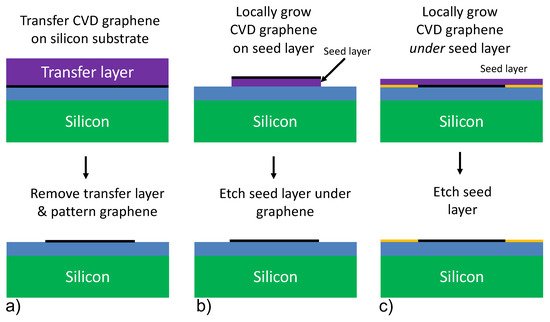
Figure 1a top). As the last step, graphene can be patterned using conventional lithography methods (
Figure 1a bottom).
Figure 1. Schematic flows for transfer-based and transfer-free integration of CVD graphene on silicon wafers. (a) Transfer-based integration flow. (b) Transfer-free integration flow, growing graphene locally on top of a seed layer (purple). (c) Transfer-free integration flow growing graphene under a seed layer, where the yellow blocking structure layer is used to define the local graphene growth region. The blue layer in the figure can be the CMOS backend SiO2 layer, or any other interface of choice.
This transfer-based CVD graphene integration route has the advantage that the growth of graphene can be optimized completely independently from the substrate, enabling high-quality graphene to be integrated, without exposing the substrate to high temperatures. However, it also poses challenges, since the transfer procedure can result in imperfections in the CVD graphene due to (polymer) contamination, membrane fracture, wrinkling, and strain non-uniformities [
4]. The grain boundaries in the polycrystalline transition metal foils or films that are used to grow the CVD graphene can also be a source of imperfections [
5]. Although transfer-based CMOS integration is still the method of choice [
2], these challenges have not been fully solved, such that actual device performance, and device-to-device uniformity continue to be limited by transfer related imperfections.
3. Transfer-Free Integration
Considering the aforementioned drawbacks of transfer-based graphene flows, it is of interest to investigate alternative ’transfer-free’ methodologies, where the graphene is grown directly on the substrate, such that the transfer process can be eliminated. However, the number of substrates on which graphene can be grown has appeared to be limited. Moreover, the high electrical conductivity and reflectivity of the transition metal substrates that are commonly used for graphene growth prohibit many device applications. A notable exception appeared to be silicon carbide, which allows direct growth of single-layer graphene on its surface and is still a strong contender for enabling graphene integration, despite the high price of crystalline silicon carbide wafers limiting production volumes.
An alternative route towards transfer-free graphene growth on silicon wafers is the use of a seed layer that is deposited on top of the substrate wafer for growing graphene. For such growth using a seed layer, the transition metals Cu, Ni, Mo and Pt, on which CVD graphene growth has been established, are logical choices. With Mo and Pt being the preferred seed materials, since Ni and Cu tend to form silicides or diffuse into the silicon faster.
During the last years, it was shown that few-layer CVD graphene can be grown on Mo seed layers [
6] that are as thin as 50 nm (
Figure 1b top). Moreover it was demonstrated that after graphene growth it was possible to remove (
Figure 1b bottom) the seed layer by underetching [
7,
8,
9]. This resulted in locally patterned, transfer-free graphene structures on the substrate that, after electrical contacting, function as gas-sensors [
7] and pressure sensors [
9,
10]. This transfer-free growth of graphene certainly has a strong potential, in particular for micromechanical sensor applications, even though it does not offer very high electronic mobility and cannot be used for growing single monolayers of graphene.
Another route toward transfer-free graphene integration is by using Pt seed layers in a process flow where graphene grows beneath the seed layer, at the SiO
2/Pt interface, as shown in
Figure 1c. This process is combining the benefits of CVD graphene growth on Pt with a transfer-free integration on silicon wafers. The process involves local graphene growth at the Pt/SiO
2 interface, after which the Pt seed layer is removed. This process reduces organic contamination, mechanical stress and other potential challenges of transfer-based process flows. Moreover, we show that an additional intermediate, adhesion layer of thin film of Ta metal between Pt and SiO
2 can locally inhibit the graphene growth with designed patterns. A similar study has been done by implementing a Ni thin film as a seed layer [
11]; however, in that work the high carbon solubility of the metal was an impactful bottleneck towards control of the number of graphene layers.
Platinum was one of the first transition metals that was used as a substrate for graphene CVD growth [
12,
13,
14,
15,
16,
17,
18,
19]. It follows from simulations that the distance between the graphene layer and the Pt substrate is 3.1 Å, which is significantly larger than that of CVD on Cu or Ni (2.24 Åand 2.01 Å) [
14,
20,
21,
22,
23]. This large distance results in a small average adhesive energy per carbon atom (∼39 meV) [
14,
20], minimizing effects of the substrate on the graphene layer. Moreover Pt is more resistant to oxidation than Cu and Ni substrates. These properties have enabled the growth of large single-crystalline graphene islands on the platinum surface.
When graphene is grown on Cu or Ni foils, the foil is often etched away after the growth process. However, Pt foils are costly, and reuse of the foils is therefore often preferred, which has led to the development of processes to delaminate the graphene from the Pt surface [
24], or grow it on much thinner Pt layers [
25]. Growth on Pt can thus yield high-quality graphene, if the transfer challenges discussed in Section 2 can be dealt with.
4. Conclusion and Outlook
Due to the difficulties related to transfer-based integration of graphene, transfer-less or direct growth approaches for integrating graphene on silicon and CMOS have been gaining growing attention. The drawback of these transfer-less schemes is however that the growth temperatures are so high that they will lead to detrimental diffusion of the p and n-type dopants in CMOS transistors. For that reason other 2D materials, that can be grown directly on silicon substrates, are also receiving increasing attention as potential materials for CMOS integration and might thus might have a better chance for playing an important role in next-generation nano-electronic devices.
This entry is adapted from the peer-reviewed paper 10.3390/ma15103723