Active remote sensing is less affected by the radiation of thermal energy from the surrounding environment. Active remote sensing has advantages of high resolutions and longer electromagnetic signal ranges, particularly for imaging systems. However, the design of active remote sensing systems is more complex; active remote sensing systems require a stable and efficient terahertz source; correspondingly, the cost is higher than for passive remote sensing systems. Passive remote sensing systems have simpler designs, do not require terahertz sources, and the costs are correspondingly lower than for active remote sensing systems. For remote sensing and imaging applications, terahertz radiation imaging is conceptually similar to optical imaging, involving the identification of objects. Object identification systems are often designed for outdoor use and strong target object penetration and backscatter, but such systems are affected by the surrounding environment. Due to the low energy magnitude of reflected or emitted terahertz signals received from the target object, terahertz detector circuits are required to have high sensitivity and require careful design to maximize the signal-to-noise ratio (SNR).
2. The Development of Terahertz Frequency Multipliers
Research associated with terahertz frequency multipliers closely follows the progress of semiconductor technology. Research on whisker-type Schottky diodes was performed in the 1970s; by the 1990s, planar Schottky diodes appeared and were widely utilized due to their high reliability, easy integration and good consistency with respect to the manufacturing process. These advantages meant wthe whisker-type as gradually replaced diode with the planar-type diode. Combined with hybrid integrated circuit technology, the planar Schottky diode became the mainstream terahertz frequency multiplier technology. After the year 2000, with the development and improvement of new materials and new processes, monolithic microwave integration technology (MMIC) became an important research direction.
The research institutions working on terahertz frequency multipliers include JPL (Jet Propulsion Laboratory) and VDI (Virginia Diodes) in the United States; Teratech in the United Kingdom; Chalmers University of Technology in Sweden; ACST (GmbH) in Germany; the Paris Observatory of France; and some scientific research institutes in China, including Southeast University, University of Electronic Science and Technology of China (UESTC), China Academy of Engineering Physics and the Hebei Semiconductor Research Institute, among others.
For the development of terahertz multipliers, different technologies and approaches have been proposed for achieving higher frequencies and more powerful output responses. Porterfield, Erickson and colleagues at JPL proposed a balanced doubler structure [
49], whereby the diodes in an anti-series configuration are placed at a junction between a waveguide and suspended microstrip to provide mode isolation. This structure has been frequently used to design frequency doublers operating at frequencies spanning millimeter waves to 1.5 THz [
50,
51,
52,
53]. For greater output power, a series of power-combined doublers have been proposed and demonstrated [
30,
54,
55,
56,
57,
58,
59]. In 2018, Siles et al. designed and manufactured a 510 to 560 GHz GaAs Schottky diode power-combined frequency multiplier [
59], with an output peak power of 30 mW. Compared with the previously reported frequency doubling technology in the same frequency band, this novel design increases the output source signal by nearly 10 times and the conversion efficiency is 8–9%. The tripler exhibits power synthesis technology and an improved epitaxial structure, and consequently the power processing capacity is significantly improved. The power synthesis technology is significantly different from the previous methods of power synthesis using discrete chip (IC, integrated circuit) technologies, since the power synthesis is achieved by directly combining two output signals on a single chip; this allows better control of the amplitude, phase consistency and symmetry of the synthesis circuit. Such broadband high-power terahertz sources can operate at room temperatures and can also be used as the receiver and local oscillator for terahertz imaging and communication systems.
When operating at a high input power, circuit self-heating effects should be considered, and different modeling methods have been proposed to characterize the temperature rise in the diode structure. These methods include transient current measurements [
60], a thermal resistance matrix approach [
40] and a physical electro-thermal model [
41]. These approaches allow for efficient and stable modeling and prediction of frequency multipliers at high operating temperatures using a harmonic balance simulator. For efficient substrate heat conduction, some substrates with good thermal conductivity have been adopted to increase the heat dissipation capacity of frequency multiplier designs; these substates include AlN (aluminum nitride) [
61,
62] and a diamond heat spreader [
63,
64]. The Rutherford Appleton Laboratory (RAL) used substrate transfer technology to transfer a GaAs Schottky varactor to an AlN substrate, and this improved the heat dissipation capacity of the circuit [
65]. A 320 GHz frequency multiplier designed by researchers at the RAL. The beam lead technology in the circuit provides the grounding for the diode and also serves as the support for the chip. The output power of the frequency multiplier is ~2 mW between 305 GHz to 340 GHz, while the maximum efficiency at 320 GHz is 13.6%.
Traditionally, many frequency multipliers have been designed using GaAs technology. However, GaN material has a wider forbidden width, and this is associated with the higher breakdown voltage and higher power-handling capability. Therefore, various research studies have been associated with the design and production of GaN-based frequency multipliers [
31,
66,
67,
68]. In 2016, Viegas and colleagues designed and manufactured a 160 GHz two-octave device based on a Schottky diode with four anode anti-series structures [
69]. The frequency doubler has three ports: an input, output and DC bias port. The reverse short circuit structure at the input is used to suppress the dominant waveguide mode TE
10 and the height-reducing waveguide structure is used at the input to suppress waveguide mode TM
11. This doubler is used an AlN substrate to provide better heat conduction within the structure. A peak output power of 35 mW has been achieved by the AlN substrate doubler with a 150 mW input power and 23% conversion efficiency.
The design of frequency multipliers requires Schottky diodes and associated passive circuit elements, including waveguide-to-microstrip transitions, impedance matching circuits and filters. If each sub-circuit is designed separately, the whole circuit may be larger than required and less efficient. Therefore, designing a frequency multiplier as one cohesive structure is a good way to alleviate certain challenges during design parameter optimization. In 2013, Guo and colleagues designed a 135 GHz to 150 GHz frequency tripler [
70] based on Schottky diodes designed as waveguide resonant filters. In the overall frequency tripler structure, the input signal and output signal of the diode part pass through the input and output probes with waveguide resonant filter structures. Therefore, the corresponding impedance matching is achieved within the filter part, and the conversion from higher-loss planar transmission to a lower-loss high-Q waveguide is achieved. In this design, the resonant waveguide provides filtering, impedance matching and a microstrip-to-waveguide transition. Moreover, the frequency tripler has an unbiased circuit structure, which is more popular for practical use.
The HBV is an important device used to generate terahertz waves. The device has odd harmonics due to having a symmetric C-V curve and anti-symmetric I-V curve [
24]. A monolithic HBV-based tripler [
26] was demonstrated with a 31 mW peak output power at 282 GHz, and a corresponding minimum conversion loss of 11.6 dB was achieved. The thermal resistance and electrical impedance of the HBV diode were assessed using 3-D FEM simulations (COMSOL Multiphysics) and experimental extraction through DC and S-parameter measurements.
From the perspective of circuit implementation, terahertz monolithic integrated circuits (TMICs) have good process manufacturing consistency compared with hybrid integrated circuits (HIC), thereby avoiding errors associated with manual assembly. At present, the TMIC is nominally utilized for the design of terahertz devices due to the high manufacturing accuracy. Table 1 gives a performance summary and comparison between the state-of-the-art frequency multipliers developed with Schottky diodes and HBVs.
Table 1. Performance summary and comparison between state-of-the-art frequency multipliers.
Using the proposed power-combined technology, the frequency multiplier devised by JPL achieves an output power up to ten times the output power of associated counterparts designed by other institutes [
71]. Ref. [
71] has summarized the power outputs of frequency multiplication sources at the time of publication (2018).
The trend summarized in [
71] shows that as the output frequency increases, the output power decreases, although there is a research trend to increase the conversion efficiency and output power at higher frequencies. At present, frequency multiplication sources at lower frequency bands can be sufficient for many designs; indeed, frequency multiplication sources are readily available at frequencies above 1 THz. However, the output power of a terahertz source has a low magnitude, so this is still an active area of research. Compared with a frequency multiplier containing a hybrid integrated structure, the use of a monolithic integrated frequency multiplier in a design can reduce the circuit error and improve the output efficiency. A corresponding thin film process and substrate-free process can also help to reduce transmission loss and improve the conversion efficiency. This is the preferred process technology for the design and fabrication of terahertz frequency multipliers. Moreover, accurate modeling of the design can improve the consistency between simulation and actual circuit tests, providing an effective way to improve the output power of the system.
3. Terahertz Remote Sensing System
3.1. Remote Sensing Applications
The first terahertz remote sensing system to be introduced was the imaging system developed by the Jet Propulsion Laboratory (JPL) of NASA (USA) with radar ranging capability in the terahertz wave band [
72]. Frequency modulation is performed using a K-band synthesizer of a single-phase prime 630 GHz scanning vector imager associated with distortion compensation technology. In the heterodyne receiver associated with the system, the terahertz transmitting source and terahertz local oscillator source are provided by a frequency-doubling chain composed of W-band MMIC (monolithic microwave integrated circuit) power amplifier modules and frequency multipliers. The signal source of the vector measurement system uses a ×36 octave chain and second harmonic down-conversion mixer. Both the signal source and local oscillator generate a signal with a tuning range of 14 GHz to 18 GHz with a pair of microwave synthesizer modules; the signal is then amplified through an MMIC amplifier after passing through a ×6 frequency multiplier. The acquisition of a 600 GHz terahertz source is achieved through a 6-octave chain. Finally, the 630 GHz single-pixel scanned imaging system achieves a range resolution of ~2 cm at a 4 m distance.
Terahertz technology also has important applications in space and atmospheric sensing [
74]. In 2004, NASA (United States) launched the Aura satellite for earth observation, and two polarized 2.5 THz radiometers were used for detection instruments. In 2007, the European Space Agency (ESA) produced a heterodyne spectrometer and edge detection was used to detect gas components. In 2017, NASA launched IceCube (Earth-1 spacecraft), an experimental 3U cube satellite used to observe fine particles forming ice clouds. At the same time, in China additional research was conducted related to terahertz radiometers, including a satellite-borne terahertz radiometer deployed on the FY-3 polar orbiting meteorological satellite and a microwave radiometer deployed on the FY-4 geostationary orbit satellite.
3.2. Development of a 220 GHz Imaging System
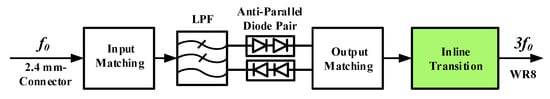
A new 110 GHz frequency tripler with a waveguide-to-microstrip inline transition based on a wedge waveguide iris is introduced here. The overall circuit structure is shown in Figure 12. The fundamental wave is input from a 2.92 mm K-connector and passes through input matching, low-pass filter, diode output matching and output probe phases. The standard rectangular waveguide (WR8) is selected as the output waveguide.
Figure 12. Circuit diagram of 110 GHz tripler with new probe structure [
75].
After the passive structure design was completed, a frequency tripler circuit structure was designed using ADS software. The SNP design file from the HFSS software was imported into the corresponding circuit structure and a SPICE model was devised for the simulation. By inputting the parameters of the dual flip chip Schottky diode DBES105a into the SPICE model, the input and output matching structures were simulated and optimized. The optimization objectives were the frequency conversion loss, return loss and output power.
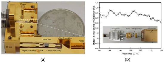
When the 110 GHz triple frequency simulation reached the level of performance required for the engineering design, the circuit was physically assembled. The final test result indicated that when a signal with a power of 100 mW was used to drive the 110 GHz frequency tripler, the average output power in the 90 GHz to 120 GHz frequency band was 3.2 mW, the peak output power was 3.67 mW, and the corresponding conversion efficiency was 2.5–3.6%. Figure 13 shows the physical processing block and measured results of the output power.
Figure 13. (
a) The physical processing block and (
b) measured conversion efficiency of 110 GHz frequency tripler with input power of 100 mW [
75].
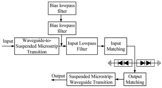
The 220 GHz frequency multiplier was designed using an unbalanced circuit topology (Figure 14). The frequency multiplier consists of E-face opening input and output standard copper waveguides, suspended microstrip lines, GaAS Schottky varactor chips and DC bias filters connected by bonding wires. The die is a flip chip placed on a 50-μm-thick quartz substrate. Four anodes of the die are arranged in anti-series for higher power output capacity.
Figure 14. Schematic of the 220 GHz tripler circuit.
When designing the entire frequency multiplier circuit, the SDM method introduced in
Section 4 was adopted. First, the HFSS software was used to simulate the linear part of the frequency tripler. Passive circuits in the design include input probe transition elements, an input low-pass filter, a DC-bias low-pass filter and an output probe transition. When designing the transition structure of the input probe, the input waveguide was appropriately widened to facilitate input matching and to shorten the length of the quartz substrate. To suppress the output of the second harmonic, the output waveguide was reduced in width. The input low-pass filter was used to suppress the propagation of the second and third harmonics generated by the diode and to allow the propagation of the fundamental input wave signal to successive stages. After the HFSS software was used to simulate different parts of the model, simulation results were exported as SNP files. The SNP files were imported into the ADS circuit simulation software, where the transmission line impedance was modified around the diode model to provide for input and output matching. Additionally, the bias voltage of the diode was adjusted. Since there is no physically accurate model of the suspended microstrip line in ADS software, the impedance and phase characteristics of the suspended microstrip line were replaced by an ideal circuit transmission line as an approximation. The impedance step change associated with the suspended microstrip line was represented by a physically accurate model and solved using 3D-EM simulation software (
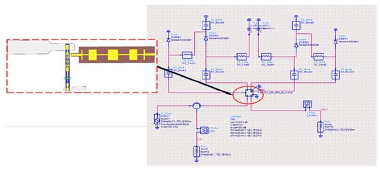
Figure 15).
Figure 15. HFSS overall model and ADS overall circuit.
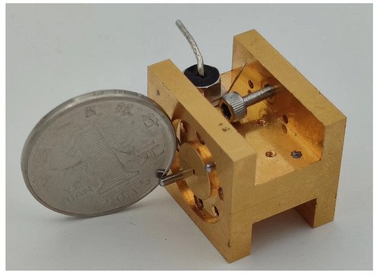
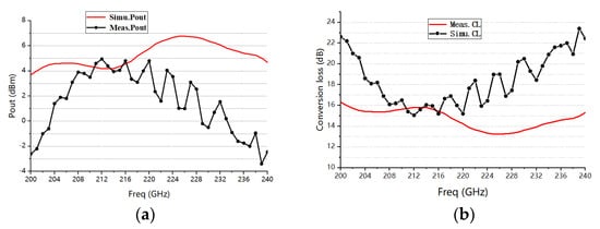
After completing the design, the tripler was fabricated and measured. The final assembled 220 GHz tripler is shown in Figure 16, with dimensions of 28 mm × 24 mm × 22 mm. The tripler was measured using a W-band power module as an input and an Erickson PM4 mm wave/sub-mm wave power meter. The maximum output power in the output frequency range of 200 GHz to 240 GHz was measured to be 3.5 mW, while the minimum frequency multiplication loss was ~15.0 dB from a 120 mW signal input (Figure 17).
Figure 16. The picture of 220 GHz frequency tripler.
Figure 17. (a) Output power at fixed 100 mW power rate. (b) Conversion loss at fixed 100 mW power.
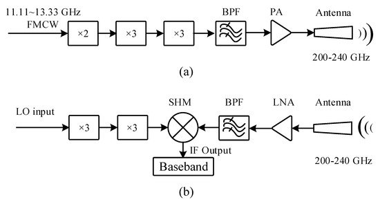
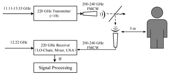
Using the novel terahertz frequency multipliers working at 110 GHz and 220 GHz and a sub-harmonic mixer at 220 GHz with planar Schottky diode technology, a remote sensing front end was developed (
Figure 18). For the transmitter channel, the final output power should be reached at around 4 dBm in the 200–240 GHz band for a 5 m detection range according to the radar principle. If the gain of the amplifier is assumed to be 15 dB and the insertion loss of the filter is 1 dB, then the output power of the 220 GHz tripler needs to reach −12 dBm. The transmitter front end is composed of a × 2 × 3 × 3 multiplication chain, whereas the low-frequency amplification and frequency multiplier segments were constructed using commercially available ICs. The last frequency tripler is the 220 GHz tripler developed with four-anode Schottky diodes that converts the 73.3 GHz signal provided by the low-frequency multiplication chain to a 220 GHz signal with a conversion loss of ~14 dB. The PA (power amplifier) was developed with an InP HBT (indium phosphide heterojunction bipolar transistor) 0.25 μm processor, and this amplifier exhibits a gain of 18 dB and a saturation output power of 5 dBm in a flip-substrate technique package [
76]. Finally, the generated FMCW (frequency-modulated continuous wave) 200 GHz to 240 GHz terahertz signal is radiated into the air by a horn antenna.
Figure 18. Block diagram of the developed 200–240 GHz FMCW terahertz remote sensing system for security check applications: (a) transmitter; (b) receiver.
The receiver front end is composed of a LO (local oscillator) × 3 × 3 frequency multiplication chain generating a 110 GHz signal with an output power of 3 mW; this includes the 110 GHz tripler developed using Schottky diodes (
Section 5). The 110 GHz tripler was used to drive the 220 GHz sub-harmonic mixer. The reflected terahertz signal was received through a horn antenna followed by a low-noise amplifier (LNA) to amplify the signal amplitude, with an average gain of 16 dB. After filtering with a bandpass filter (insertion loss of 1 dB), the signal is injected into a sub-harmonic mixer and down-converted to an IF (intermediate frequency, 1–3 GHz) signal with a SSB (single sideband) of 9–10 dB. Finally, the IF signal is processed by a baseband platform that includes digitization.
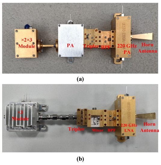
The final established 200 GHz to 240 GHz FMCW terahertz transceiver imaging front end is shown in Figure 19. Figure 19a shows the 220 GHz frequency multiplier transmitter chain, delivering a 200 GHz to 240 GHz FMCW signal through an 18-times frequency multiplication and amplification chain. Figure 19b shows the 220 GHz receiver composed of a 110 GHz LO chain, 220 GHz sub-harmonic mixer, filters and 220 GHz LNA (low-noise amplifier).
Figure 19. Photograph of the fabricated 200–240 GHz remote sensing system for imaging applications: (a) transmitter channel; (b) receiver channel.
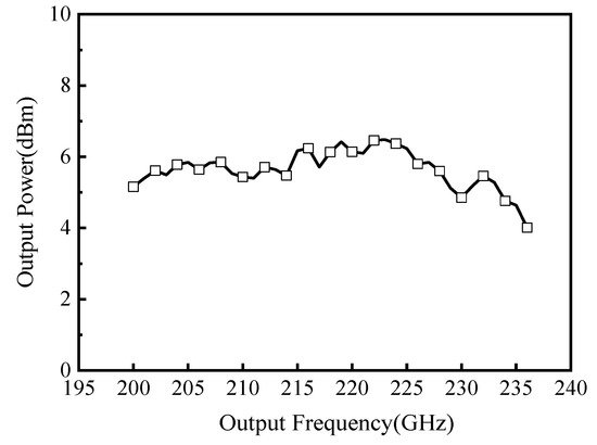
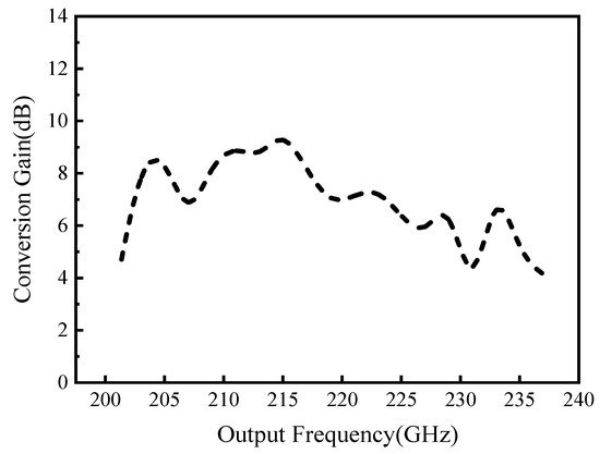
The 220 GHz transmitter and receiver were characterized and tested separately before combining the transmitter and receiver into an imaging sensor system. The transmitter delivers an output power of 5.2 dBm across a 200 GHz to 236 GHz range, with a peak output power of 6.5 dBm at 223 GHz (Figure 20). The mixer and LNA were characterized using the Y-factor method and found to exhibit noise temperatures of 2958 K for the mixer and 924 K for the LNA. When the IF of the mixer was fixed to 1 GHz with a sweep source and LO frequencies, an average 7.1 dB double-sideband (DSB) conversion gain was measured for the receiver between 200 GHz and 240 GHz, while the maximum conversion gain was 9.7 dB (Figure 21).
Figure 20. Output power of the 220 GHz transmitter.
Figure 21. Output power of the 220 GHz transmitter.
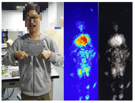
To evaluate the effectiveness of the 220 GHz FMCW remote sensing system, a preliminary test platform was built, and a block diagram of the platform is provided in Figure 22. The transmitted initial signal (11.4 GHz to 12.1 GHz) was generated by a direct digital synthesizer (DDS) chip, then the generated signal was multiplied 18 times to the 205.2 GHz to 217.8 GHz range and radiated into the air using a horn antenna. A secondary reflection mirror was used to focus the THz beam to obtain an image. A person held a 40 cm by 25 cm metal plate in front of their chest and stood 5 m away from the horn antenna (Figure 23). The reflected signal detected by the received antenna was converted into an IF signal and digitized using a custom-designed digital signal process (DSP) subsystem. As shown in Figure 23, the image of the 220 GHz remote sensing system in the spatial vicinity of the metal plate shows a significant brightness difference between the metal plate, the surrounding clothing and human body tissue.
Figure 22. Schematic diagram of the 220 GHz remote sensing imager.
Figure 23. Imaging results of the 220 GHz terahertz front end for a 5 m stand-off distance.