1. Phase-Change Memory
Phase-Change Memories (PCM) are the most advanced and front runners in the field of nonvolatile memories. They are part of a Chalcogenide family (primarily Group VI elements) based two-dimensional material sandwiched between two metal electrodes, and a resistive electrode referred to as heater [
68,
69]. Most commonly studied ones are the Ge-Sb-Te (GST) class of materials [
70,
71,
72]. The presence of two distinct solid-state phases, i.e., crystalline and amorphous, with contrasting electrical and optical properties, makes them an attractive choice. The dynamic switching between amorphous-to-crystalline phases of the material in the presence of electrical pulses is used to model neuron’s integration and firing behavior. When the PCM material is in the amorphous phase, it has high resistance (i.e., the high-resistance state HRS). The PCM crystallizes by applying medium voltage electric pulses. This represents the device’s SET operation, which incrementally increases the amorphous layer thickness and is used to model the temporal integration of membrane potential in a neuron implementation. When the PCM reaches a full crystallization state, the device presents a low resistance (i.e., low-resistance state LRS). The LRS is used to model the neuron’s threshold. Upon reaching it, the neuron fires (i.e., the device is in the LRS). Under high voltage short electric pulse, there is a generation of high current densities at the interface of the heater and the PCM material creating a Joule heating effect. This is used to perform the RESET operation after the emission of an action potential (i.e., a spike). The Joule heating is responsible for switching the crystalline phase back to the amorphous phase. The RESET is an abrupt process of melting and quenching followed by rapid cooling of the material.
To read the PCM state, we applied a low voltage in the OFF region of the device, which, in turn, produces a readout current. The switching speed determines the write speed from the amorphous to the crystalline phase, and the SET operation determines the operating step speed of this device. Recent studies show that PCM devices have a write speed to the order of 100 ns, performing better than Flash memory at lower voltages [
73]. One of the unique advantages of PCM, unlike Flash memory, is the possibility to overwrite memory without the need of erasing. Nevertheless, the RESET of PCM requires high write power due to the heat-dependent switching mechanism. Since programming in the SET state is incremental with repetitive pulses slowly increasing the mushroom type switching volume, PCM can also be used to represent multiple intermediate states between fully-crystalline and fully-amorphous [
74]. This gives the capability to store multiple bits in a cell encoded in intermediate states. In [
75], a triple-level PCM array of 64 k cells is demonstrated by Milos et al. on a 90 nm CMOS baseline chip with permutation encoding to shift the threshold of each level considering the shift in drift resistance. These devices are popularly known as PCRAM, Lance-type, or Ovonic unified memory.
Considering their high ON/OFF ratio, PCMs can also be employed as synapses with inexpensive and high-speed information transfer. In [
77], Kuzum et al. use repetitive pulses to achieve a PCM-based synapse. Here, each of the top and bottom electrodes are sent presynaptic and postsynaptic pulses, respectively. The difference in the pulse potential is applied to the memristor whose resistance stores the synaptic weight. When the presynaptic electrode spikes later than the postsynaptic electrode, the potential difference leads to the amorphization of the device. This mechanism has a perfect resemblance with the spike-timing dependent plasticity (STDP) learning rule [
78].
A two-PCM approach is proposed to implement both long-term potentiate (LTP) and long-term depression (LTD) modes of STDP [
79]. However, controlling the abrupt transition in the RESET process on multiple devices simultaneously is difficult to achieve as it requires extra circuitry. Kuzum et al., in [
80], use pulses of varying amplitudes to program SET and RESET using a single PCM cell. In this work, both potentiate and depression branches of the STDP learning are implemented per synapse. In [
81], Yi et al. show that configuring pulses at different time windows can be utilized to break down STDP into its four different variants.
The integration of PCRAM in a crossbar array facilitates large-scale storage and in-memory computing. However, writing to PCM cells in a crossbar array can incur programming current sneaking to nearby cells producing undesirable results [
82,
83]. Selector devices can avoid sneak path currents. The resulting crossbar can be in 1T-1R, i.e., one transistor one memristor, or 1S-1R, i.e., one selector diode and one memristor arrangement. In [
84], Eryilmaz et al. demonstrate STDP for simple patterns with a 10 × 10 crossbar with 1T-1R PCM cells. However, in-situ training on NVM hardware has lower accuracy than software. In [
85], Ambrogio et al. demonstrate a hardware-software approach of neural network implementation for complex image recognition. The 3T-1C cell array of hardware with supervised learning schemes implemented in software has similar accuracy as software-based schemes while being more energy efficient and fast.
At the system level, the high current requirement of PCM devices leads to thermal [
83] and reliability concerns [
86,
87]. In [
88], Balaji et al. show that in order to generate currents in a PCM crossbar, the charge pumps need to be operated at an elevated voltage, which accelerates the aging in its transistors. In [
89], Song et al. show that high aging in the CMOS device of a neuron in a PCM crossbar can lead to a lower lifetime. This is due to the high voltage operations needed to generate the SET and RESET currents in the PCM crossbar. Finally, in [
90], Song et al. show that prolonged execution of machine learning workloads on a PCM crossbar can lead to timing failures due to circuit degradation.
Even though a crossbar architecture is more compatible for implementing spiking neural networks, every PCM device in a crossbar is in series with a selector device that generates the RESET current. Thus, downscaling of PCRAM and the selector device must ensure that the selector can produce enough current to RESET the PCRAM cell. This scaling limitation of PCRAM can be solved by shrinking the heater-PCM interface region [
91] or cell structures with advanced device engineering [
92]. Several alternative selector devices such as BJT, diodes, and Schottky diodes are used to alleviate the potential problem of producing adequate heating resistance that instigates the Joule heating. One such device is mixed ionic-electronic conduction (MIEC), which is used for 3D integration [
93].
2. Resistive Ram
Much like PCM, Resistive Random-Access Memories (RRAM) have been explored in depth by many since the discovery of variable resistance anodic oxide materials [
97,
98]. The dynamic of RRAM is governed by the switching of a metal–insulator–metal (MIM) structure where the insulator can be an oxide or an electrolyte. The switching could be caused by thermo-chemical effects, which induce unipolar structures, or nano-ionic redox effect induced bipolar structures. Bipolar devices show conducting and insulating behavior for opposite bias applied on the two metal electrodes. Usually, both electrodes are active. However, in the case of an electrolyte insulator, one of the electrodes remains inert.
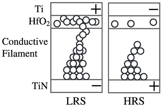
Figure 1 shows an RRAM cell, where the insulating film (
HfO2) is placed between two conducting electrodes forming the MIM structure. The left subfigure shows the formation of LRS states using the conducting filament. The right subfigure shows the depletion of the filament on application of a negative voltage to the top metal. This represents the HRS state.
Figure 1. Operation of an RRAM cell.
Consider an RRAM cell that is initially in the high-resistance state (HRS). Then, with the application of high forming voltage, the RRAM cell switches from HRS to the low-resistance State (LRS). This is the SET operation of RRAM. Unlike PCM, RRAM works as an integrated unit when connected in parallel with a capacitor in an RC circuit. This forms the basis for the implementation of a leaky-integrate-and-fire (LIF) neuron [
99]. For a leaky-integrate-and-fire (LIF) neuron, the membrane potential can be modeled as the concentration of oxygen vacancies. During the voltage sweep measurement of MIM structures, the dielectric breakdown leads to a jump in the current, which could be converted into an analog spike output. Several switching mechanisms have been discovered in recent years, some of which are discussed below.
Filamentary RRAMs are composed of those oxides that form a chain of defects that can act as a filament. These defects are formed due to thermal redox reactions between the metal and oxide interface. Forming the conductive oxide path in the presence of a high electric field displaces the oxygen atoms from its lattice, creating vacancies.
Nonfilamentary RRAM, on the other hand, are devices in which defects migrate to the Schottky barrier of the metal/oxide interface. Defects change the functionality of the material with additional defect energy bands in the energy diagram of the device, resulting in resistance change. In [
103], Hansen et al. demonstrate a double barrier memristive device with oxide tunnel barrier and Schottky barrier. They show that nonfilamentary-based switching has improved retention compared to filamentary devices. In [
104], Yang et al. alter the frequency to transition from Short-Term Plasticity (STP) to Long-Term Plasticity (LTP) in the inorganic
WO3based synapse. When the pulse width is reduced to achieve a higher frequency, the memorization strength of the nonvolatile memory increases. Implementation of STP and LTP with a single device indicates the resemblance of the artificial nanodevice to a biological synapse.
When a positive bias is applied to the anode, metal ions start drifting to the cathode, leading to a reduction (oxidation) at the anode (cathode). Accumulation of metal ions at the cathode forms a filament incrementally. An opposite bias breaks the growth of the material. In [
106], Fackenthal et al. demonstrate a three-layer Cu-based chip with a 16 GB array of memory cells divided into an architecture composed of eight tiles for commercial use. In [
107], Wijesinghe et al. implement the functionality of a deep stochastic spiking neural network (SNN) on a 32 × 32 crossbar with CBRAM memristors. The proposed design is compatible with any ANN network producing similar accuracy for less energy consumption.
RRAM’s read disturbance issues create system-level challenges for the successful deployment of RRAM in neuromorphic architectures [
108]. The authors show that if the read disturbances are not incorporated during the mapping of deep learning models, the correct operations of the device over its lifetime can significantly be reduced [
109,
110]. To address this, model parameters need to be reprogrammed periodically, which leads to high system overhead [
111]. Like PCM, RRAM also suffers from resistance drift, which is also recently studied [
112]. Recently, authors reported the latency overhead of RRAM’s multilevel cell operation and its system-level implications [
112].
Another technological challenge of RRAM is represented by the interactions at the metal-electrolyte interface, which reduce the reliability of CBRAM [
113]. There also exists a tradeoff between programming speed and retention in nonfilamentary RRAM. Higher switching speed is achieved with a low energy barrier, but this might limit the operating range to a certain time domain [
114]. Material engineering to use thinner insulator layers can address this issue. However, filamentary RRAM shows significant variability due to considerably short switching time [
115]. Furthermore, device and material engineering that provides better control over the conductance update of the device is required.
3. Magnetoresistive Ram
Resistive and phase change memory cells suffer from degradation over time and limited endurance cycles. Magnetoresistive RAM (MRAM) alleviates this issue by providing almost unlimited endurance with a fast switching mechanism [
116]. Instead of exploiting device physics as in PCM and RRAM, MRAMs are the class of memristors that exploits memristive properties, e.g., via a change in the magnetic state of the device, also known as magnetoresistance. The magnetoresistance property is very similar to the operation of a hard disk drive. Since magnetic polarization is independent of the power supply, it behaves as nonvolatile memory. Switching in MRAM is governed by the spin dynamics of electrons, and it does not involve any movement of subatomic particles making it less subjected to wear-out.
Magnetic Tunnel Junction (MTJ) is the first device to utilize electron spin as a memory storage variable [
117]. MTJ comprises two ferromagnetic nanomagnets with a dielectric layer in the middle. This composition is the same for all other devices discussed below. However, in MTJ, one nanomagnet has fixed magnetic polarization, and the other is free. Current induced switching between parallel and anti-parallel states transfers the spin to nanomagnets [
43].
In Spin Transfer Torque (STT) MRAM [
118,
119], the magnetization changes due to torque transfer from incoming electrons. Continuous application of input spikes is integrated to switch the polarization of magnetizing material. In [
120], Rezeszut et al. usea multi-bit STT-MRAM cell as a synapse to recognize the MNIST database. The I-V curve was tuned to simulate seven serially connected MTJs to represent 8-bit data. The proposed design requires no additional hardware with programmable MTJ multi-cells comparing the input to enable positive or negative weights. A select transistor could also be used for the same. The neuron circuit combines MTJ synapse, differential amplifiers, and a sigmoid function generator.
Recently, Spin-Orbit Torque (SOT) MRAM has gained interest due to its high spin injection efficiency [
121]. SOT-MRAM switches due to domain wall movement by an orthogonal current through underlying heavy-metal layer [
122]. In a proposed 4T synaptic device, the spin-orbit torque generated in the heterostructure mimics STDP behaviors. The programming current is linearly related to the domain wall position, and it is responsible for inducing a conductance change. However, a low programming current could better modulate conductance because of higher spin injection with ultra-low energy consumption. In Spin-Transfer Torque MRAM (STT-MRAM), read and write have the same path, with reading resistance affecting the write path. SOT-MRAM, on the other hand, has separate read and write paths. This improves the speed of operation. In [
123], Ostwal et al. implement a deep belief network with SOT-MRAM synapses.
Apart from STT- and SOT-MRAM, Domain Wall Magnets (DWM) are promising MRAM devices that could be used both as neurons and synapses [
124]. Committed to the elastic coupling phenomenon, it has a similar composition of opposite magnetic domains separated by a domain wall. The input current generates torque that communicates with the magnetic moment of the ferromagnet to move the domain wall in the direction of the current flow. The attempt to align the magnetic moment of the ferromagnet shits the position of the domain wall. Controlled shifting can lead to multiple resistance states. A DWM-MTJ device can replicate synaptic behavior where MTJ at the extreme end of DWM is used as a polarity sensor. In [
125], Sengupta et al. implement an all-spin neuromorphic architecture with spintronic devices made of an MTJ whose free layer is a DWM. This ferromagnetic-heavy metal configuration is known to show deterministic domain wall shifting. The authors also demonstrate a crossbar with synaptic device domain wall position storing the weight information.
The challenge with large-scale spintronic neuromorphic hardware is the low-resistance ON/OFF ratio. Although these devices provide unlimited endurance, high-speed operation at low power consumption in a single MRAM cannot show competitive resistance ratios. This implies that the read resistance can significantly affect the write paths. The development of efficient sense amplifiers to sense such low-resistance differences will be required. However, it is more compatible with dense networks with its CMOS integration, long-range communication, and multi-layer nature [
126].
4. Ferroelectric Fet
Ferroelectric materials are a family of crystalline materials that exhibits the formation of electrical dipoles that can switch polarization with an applied electric field. Moreover, a sub-family of these materials presents a nonvolatile hysteric window of operation that, when coupled in series with a gate of a MOSFET or FinFET, can be used to reproduce nonvolatility behaviors [
127]. Thus, a sufficient thick Fe layer is required to establish a hysteric I-V characteristic [
128]. When a positive bias induces an electric field greater than the coercive field, Fe can be downward polarized (in certain scenarios), turning the FET ON with the channel in inversion mode of low resistance [
129]. A negative bias on the top electrode turns the FET OFF with the channel in depletion mode of high resistance. One unique advantage of FeFET devices is the read and write operations are voltage based, unlike PCM or MRAM current-controlled memristors. However, the FeFET memory cell has a destructive read cycle, where data are read by altering a bit in each cell. Even a small current can sometimes indicate the cell is in the OFF state.
In [
130], Mulaosmanovic et al. demonstrate ferroelectric HfO
2in a FeFET device to function as a neuron. Application of identical pulses below the electric field’s threshold value accumulates its nano-domains until the threshold is reached. At this point, the device manifests an abrupt switching behavior to the opposite polarity domain. This switching behavior is the result of the accumulative nucleation of nano-domains acting as a perfect integrator. Arrangement of FeFET as a memory array could turn ON cells that are not supposed to be active due to the accumulative excitations on the shared bit line. In [
131], Mulaosmanovic et al. implement STDP using a single two-terminal FeFET in series with a resistor as a synapse. The resistor connected between the gate and drain ensures the development of an electric field for ferroelectric switching. Pulse amplitude and width modulation facilitate threshold tuning of the device. The time difference between presynaptic and postsynaptic spikes controls the potential drop. Authors show that Increased drop generates inclement charge flow between neurons modeled as asymmetric STDP.
A three-terminal FeFET provides better control with separate read and writes paths facilitating simultaneous updates [
132]. Here, a neural network of nine neurons and twelve synapses is fabricated to recognize a 3 × 3 matrix pattern. The temporal offset between the presynaptic and postsynaptic spikes is passed through a CMOS selector as the gate voltage. The 3T-FeFET exhibits STDP behavior on a Hopfield neural network. Although FeFET is more compatible for integration with CMOS technology, not all ferroelectric materials have a stable growth on CMOS. Recently, crossbar structures have been simulated on HSPICE models [
128]. In [
133], Chen et al. demonstrate a FeFET-based crossbar array in 2T-2R design. Here, each cell performs an XNOR operation.
Ultra-low-power operation and easy integration of ferroelectric materials need more optimized circuit architectures to build large-scale neuromorphic systems.
5. Nanowires
In addition to memristors that work based on the individual device switching, nanowires similar to CNTs attain storage capability due to intercommunication. Although intercommunication in PCMs and RRAMs is disregarded as sneak path current. Nanowires are evaporation deposition on the desired substrate material with metal electrodes. Electrical excitation causes the movement of metal ions in a one-dimensional structure to fill the nano-gap. These nanometer thickness wires from group-IV and group III-V show semiconducting behavior due to physiosorbed redox molecules [
129]. Apart from these, there are several inorganic and organic molecular-based nanowires reported in the literature. Nanowires, when used in conjunction with other nonvolatile memory elements, have great potential to emulate biologically plausible topology and connectivity [
126].
A single nanowire in its simplest form shows nonvolatile memristive nature due to the formation of metallic filaments across an insulating shell layer. The electrochemical interaction between nanowires exhibits storage functionality. In a recent work [
134], authors demonstrate Ag-SiO
2nanowire networks in a bottom-up approach that can reweight and rewrite. At a nanowire cross point, the application of electrochemical potential diffuses Ag+ ions in the insulating shell layer to form a conductive bridge. This process of formation/rupture is utilized as reweighting. Further, the nanogap developed due to the breakdown of electromigration effects can potentially act as sub memristive elements rewiring to implement plasticity. In [135], Li et al. demonstrate the biological phenomenon of winner-take-all conductivity pathway creation based on memristive interactions. Ag nanowires with TiO2
coating were studied for pathway formation using the lock-in thermography (LIT) technique [
136]. Triangular pulses at one of the metal electrodes produced current hysteresis, with a switching accordant LRS and HRS states where LRS is the formation of at least one pathway of a nanowire-nanowire junction. However, the power dissipation observed in LIT is due to Joule heating or internal heating of the device. These architectures have also proven to be effective in unconventional computing paradigms like Reservoir computing.
This entry is adapted from the peer-reviewed paper 10.3390/electronics11101610