A complete view of basic principles and mechanisms with regard to improving the structure stability, physical and chemical properties of the low dimensional semiconductor-based photocatalysts is presented here. Various 2D semiconductor-based photocatalysts show a high electrochemical property and photocatalytic performance due to their ultrathin character, high specific surface area with more activity sites, tunable bandgap to absorb sunlight and versatile options in structural assembly with other nanosheets. At present, most photocatalysts still need rare or expensive noble metals to improve the photocatalytic activity, which inhibits their commercial-scale application extremely. Thus, developing less costly, earth-abundant semiconductor-based photocatalysts with the efficient conversion of sunlight energy remains the primary challenge. A concise overview of different types of 2D semiconductor-mediated photocatalysts is given to figure out the advantages and disadvantages for mentioned semiconductor-based photocatalysis, including the structural property and stability, synthesize method, electrochemical property, and optical properties for H2/O2 production half-reaction along with overall water splitting.
- Ultrathin semiconductor-based photocatalysts
- Hydrogen evolution reaction
- Oxygen evolution reaction
- Overall water splitting
Abstract
Ultrathin two-dimensional (2D) semiconductor-mediated photocatalysts have shown their compelling potential and have arguably received tremendous attention in photocatalysis because of their superior thickness-dependent physical, chemical, mechanical and optical properties. Although numerous comprehensions about 2D semiconductor photocatalysts have been amassed, up to now, low-cost efficiency, degradation, the kinetics of charge transfer along with recycling are still the big challenges to realize a wide application of 2D semiconductor-based photocatalysis. At present, most photocatalysts still need rare or expensive noble metals to improve the photocatalytic activity, which inhibits their commercial-scale application extremely. Thus, developing less costly, earth-abundant semiconductor-based photocatalysts with the efficient conversion of sunlight energy remains the primary challenge. This review begins with a brief description of the general mechanism of overall photocatalytic water splitting. Then a concise overview of different types of 2D semiconductor-mediated photocatalysts is given to figure out the advantages and disadvantages for mentioned semiconductor-based photocatalysis, including the structural property and stability, synthesize method, electrochemical property, and optical properties for \( \rm H_{2}/O_{2} \) production half-reaction along with overall water splitting. Finally, we conclude this review with a perspective, marked on some remaining challenges and new directions of 2D semiconductor-mediated photocatalysts.
1. Introduction
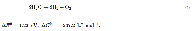
Nowadays, the biggest technological challenges for human beings are the increasing consumption of resources and energy and the related environmental pollution problem all over the world. For example, the worldwide energy consumption will expect to reach up to 815 quadrillion Btu in 2040 due to the growing global production and population [1,2]. However, the huge energy resources in the earth mainly originate from non-renewable coal, oil, natural gas, and nuclear energy, and their reserves are limited. Although the energy is released by combustion on the application of these fossil fuels, a series of critical environmental problems—water contamination, greenhouse gas emissions, global warming, and the emergence of a hole in the ozone layer—occur at the same time. Thus, lots of scientists, politicians, industry groups are encouraged to seek new and sustainable alternative energy resources. Every day the sun radiates an enormous amount of energy for our planet, which has attracted great attention as a promising alternative energy source for cutting greenhouse gas emissions and providing the current and future human energy demand. However, it is not nearly sufficient, therefore, the harvest and conversion of solar energy into other kinds of energy is a priority to resolve [3,4,5]. At present, photovoltaic cells are already a popular sight on rooftops to directly convert solar energy into electricity. However, electricity presents its own challenges in that it would have to be used immediately or be stored in a secondary device at a high energy density, such as capacitors or batteries. In comparison with converting solar energy into electricity, synthesizing storable, transportable chemical fuels via photocatalytic processes would be a more attractive approach, in which the harnessing of energy in sunlight would be stored in the form of molecular bonds through a thermodynamic "uphill reaction" (see Equation (1)). Up to now, a photocatalysis technique has been used in different application fields, such as water splitting to produce hydrogen [6,7], sterilization [8], wastewater treatment and self-cleaning materials [9], decomposition of crude spills [10,11], dye-sensitized solar cell and inactivation of cancer cells [12,13].
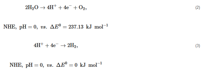
Hydrogen (H2) is a clean and carbon-free fuel with high specific enthalpy. Whereas, until now, around 95% of the world’s hydrogen fuel is mainly sourced from natural gas, by reacting methane with steam using fossil fuel to produce hydrogen and carbon dioxide (CO2). Thus the production of hydrogen from methane is a kind of fossil fuel product rather than renewable energy. The critical method to utilize hydrogen production is developing an effective H2-preparation approach without ever seeing fossil fuels. The method using photocatalytic materials to produce hydrogen has been demonstrated since 1972 according to the following reaction equation,
This photocatalytic process is driven by a thermodynamic “uphill reaction” of solar energy with a large change of ΔG
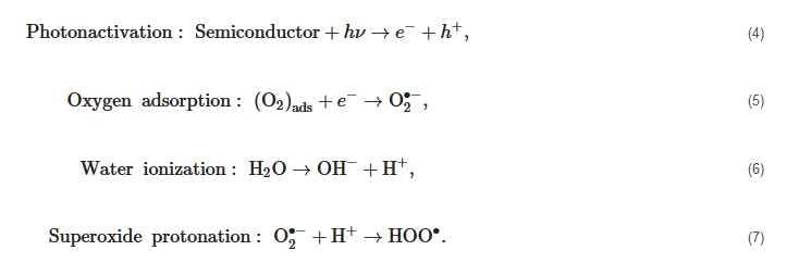
Therefore, the surface of the photocatalytic materials should be struck using suitable energy with the corresponding photons. The estimated solar photon flux density (Q) is 2000 μmols−1m−2 [15]. While the previous reports found the holes took less than 2 μs to react with the water vapor while the oxygen took 10–100 μs to capture the electrons in P25 TiO
There are three major steps to overall photocatalytic split water for a semiconductor photocatalyst: (1) the absorption of photons on the surface of a semiconductor, with appropriate energy, which can stimulate electron transfer to the conduction band position from the valence band position and generate electron-hole pairs (e−−h+), (2) the separation and migration of charge carriers on the surface of the material at a short span of time; (3) the impingement between the corresponding free electrons and holes on the surface of the system to complete the water-splitting reaction to generate H


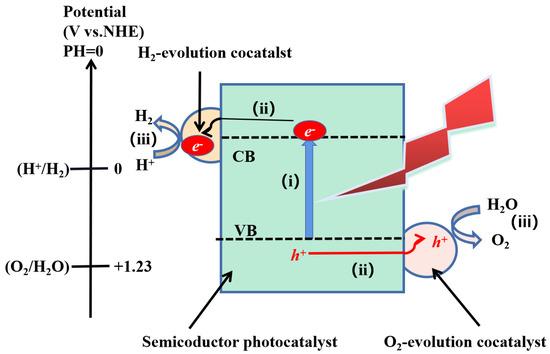
Figure 1. Schematic diagram of the three major steps of overall photocatalytic water splitting on a semiconductor photocatalyst [18].
On the other hand, nanoparticles, porous nanospheres, and nanowires have recently attracted a large amount of attention in the process of water splitting in that they possess unconventional and fancy physical and chemical properties, which may be easier to meet the requirements for overall photocatalytic splitting water compared to their bulk counterparts [30,72,73,74,75,76]. First, these different nanostructures could decrease the rate of charge carriers recombination and let them travel a very small distance, which largely enriches the selectivity of photocatalytic materials and paves a new path to design an effective photocatalysis. Second, 2D nanostructured photocatalysts could have more active sites for electrochemical reactions due to their larger surface areas. Third, quantum confinement effects in 2D metallic and semiconductor nanostructures dependent on the size and morphology of photocatalysts could open a new approach to engineer the processes of sunlight harvesting. It is because the quantum size effects can restrict electrons in order to accommodate the additional atom, platelike nanoparticles, disk, or cluster, resulting in an increase of energy levels and HOMO-LUMO bandgap. For 1D quantum confined materials, it is found that the modification of the aspect ratio of nanorods could largely tune the optical response properties [77]. Last but not least, various 2D nanomaterials provide more sources to integrate heterogeneous structures with multiple functional properties. On the other hand, for the majority of 3D semiconductors, it is commonly ignored to distinguish the electronic and optical bandgaps due to the small exciton binding energy. While the distinction between electronic and optical bandgaps in 2D nanomaterials is significant and obvious. The Bethe–Salpeter equation is frequently used to predict the exciton binding energy and optical bandgap. Furthermore, most of the 2D materials exhibit more soft elastic constants, which could have extra application compared to bulk 3D counterparts. Particularly, the band edge positions and bandgaps are very sensitive to small strains with a significant extent, thus it could facilitate tuning the photocatalytic performance of 2D nanomaterials as photocatalysts. Herein, the current review work covers the fundamental mechanism of overall photocatalytic water splitting and recent progress in the use of two dimensional (2D) semiconductor-based nanomaterials and their nanoheterostructure composites with a focus on the relationship between the structural property of the nanomaterials and their photocatalytic activity. It begins by introducing the various mechanisms of photoexcited carriers on different 2D semiconductor-based nanomaterials during photocatalytic overall water splitting to provide a whole view for the principle of work on the basis of thermodynamics half-reactions. Then, we compare the general structural property, advantages in electronic and surface properties, and electrochemical performances to pursue high efficiency of water splitting on the different 2D semiconductors, including carbon nitride (
2. Mechanisms of Overall Photocatalytic Water Splitting
In previous researches, the mechanisms of 2D and 3D materials as photocatalysts to split water have been extensively reported. With regard to semiconductors, the absorbed photon should possess higher energy (hν) than the corresponding bandgap of the semiconductor in order to excite the electrons to the empty conduction band (CB) position from the filled valence band (VB) position of the semiconductor photocatalyst. Then the excited electrons and holes pair (e−−h+) is formed according to the following expression,
The bandgap of a single semiconductor photocatalyst should meet the requirements of reduction reaction potential with 0 eV for catalyzing H
In a system with a semiconductor electrode immersing in an electrolyte solution, the electrons transfer take place spontaneously in order to keep the balance between the Fermi level (


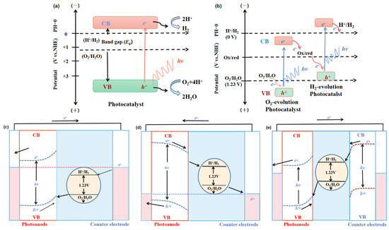
Figure 2. Energy schematic diagram based on (a) one-step water splitting and (b) Z-scheme mechanism; and photoelectrochemical water splitting using (c) a photoanode, (d) photocathode, and (e) photoanode and count electrode in tandem systems for photocatalytic water splitting, respectively [81].
3. Classification of 2D Semiconductors for Photocatalysts
To date, a great amount of 2D nanosheets have been synthesized by various chemical and/or physical methods, which are mainly divided into two types, layered and non-layer structural materials. With regard to layered materials, the in-plane layer is formed by connecting the in-plane atoms by strong chemical bonding. However, the weak van der Waals interaction plays an important role in stacking these monolayers to form bulk crystals [82]. The representative layered material is graphite crystal, which is stacked by many graphene layers via weak van der Waals force. In addition, nitrides (such as g-C
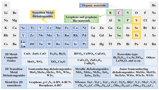
Figure 3. Periodic table with highlighted elements for typical ultrathin 2D materials.
4. Synthesis Methods for 2D Materials
Various approaches have been explored to synthesize 2D monolayers or few-layer nanosheets and tailor the structure with corresponding physical and chemical properties in order to suit different kinds of applications. Generally, the synthesis methods can be classified into two types based on the composition, crystal phase, and surface property of materials: (1) the top-down method, which mainly depends on the exfoliation of 2D monolayers from their parental layered bulk material by overcoming the weak interlayer binding force; (2) the bottom-up method, which is more versatile in principle than most 2D nanosheets, might be gained by this method. In this section, some representative methods to prepare 2D materials are discussed and summarized.
4.1 Micromechanical cleavage using scotch tape
Micromechanical cleavage using scotch tape is a simple and conventional method to fabricate thin flake by peeling and rubbing the surface of inorganic layered bulk materials. The weak van der Waals interaction between the layers of the materials is the key factor so that the applied mechanical force can peel of single or few layers of 2D materials without breaking the chemical bonding of the in-plane layer. The micromechanical cleavage technique is first used by Grim et al. to obtain graphene monolayer from highly oriented graphite [301]. Besides, a more thin flake can be obtained by repeated several times of this process. Then these thin flakes are washed with acetone and transferred on a clean, flat target surface of SiO


This micromechanical cleavage technique is simple, fast, and low cost, and the size of exfoliated 2D materials can be up to tens of micrometers. Besides, no chemicals are utilized but the shear force is applied during the fabrication process. Thus, the fabricated nanosheets keep the pristine structural integrity with minimum defects from the parental bulk materials, giving rise to many advantages. As a whole, the large lateral size, clean surface, "perfect" crystal quality, high crystallinity make mechanically cleaved 2D materials as remarkable candidates to investigate the corresponding mechanical, electronic, and optical properties and application in electronic and optoelectronic devices. While there are some certain disadvantages that hinder their realistic applications. First, the production yield of this process is extremely low and the nanosheets always coexist with thick flakes on the substrate. Thus, it is suitable for laboratory scale studies but difficult to utilize in various high-end technological applications, high yield, and large-scale production. Second, the fundamental/intrinsic properties, such as size, thickness, and shape of the ultrathin 2D nanosheets are unstable and uncontrollable since the mechanical exfoliation technique by hand is a shortage of precision and repeatability. Third, the utilized substrate is significantly important in the fabrication process. Recently, one advanced micromechanical cleavage method is reported by Sutter et al. to improve the production yield and increase the surface area of graphene and Bi
4.2 Liquid exfoliation
Liquid exfoliation actually also relies on the mechanical forces since the original idea of this technique is to apply the proper mechanical force on layered bulk crystals dispersed in a liquid to exfoliate them into single- or few-layer 2D nanosheets. Thus this technique is mechanical force-assisted liquid exfoliation which can categorize into sonication-assisted liquid exfoliation and shear force-assisted liquid exfoliation. Compare to mechanical exfoliation of 2D nanosheets, liquid exfoliation is a reliable method with high quality and large quantity to produce mono and few-layer 2D sheets at bulk scale. Up to now, the exfoliation method in liquid media has been largely reported to gain ultrathin 2D materials from for their parental layered bulk crystals, such as MoS
Sonication-assisted liquid exfoliation is an established technique using the simple and common mechanical force to peel the layered bulk materials into 2D sheets in liquid media, in which the bulk crystals are dispersed into a polar solvent and washed using bubbles induced by sonication in the solution. The cavitation bubbles generated by high energy ultrasonic waves could create high energy during the sudden burst with the release of pressure, hence the resultant dispersion is centrifuged to exfoliate of layers in the solution. It is to be noted that the key parameter is the surface energies between the layered bulk materials and the liquid system should be matched. It is because the solvents have the surface tension, using the surface tension of solvent similar to the surface energy of layer bulk crystals could reduce the energetic cost of exfoliation and prohibited the restacking and aggregating between the 2D layers [82,319,322]. For example, it is reported that pure water or pure ethanol is not an efficient way to synthesize TMDs nanosheets due to the large surface energy of the solvent, but the mixing water with ethanol could effectively exfoliate and disperse TMDs. Thus, choosing the optimum solvent could largely utilize the potential of this technique. Besides, the sonication time and centrifugation rate are also significant factors that are related to the quality and quantity of 2D materials. This method is first used to exfoliate graphite into graphene in 2008 [323]. They reported no complicated equipment or expensive chemicals is used during their experiment. Subsequently, more than 25 solvents were studied to naturally exfoliate of 2D nanosheets based on crystallinity, thickness, size, and yield of the resultant layers [319]. It is summarized that dimethylformamide, cyclohexyl-pyrrolidinone, N-methyl-pyrrolidone, Ndodecyl-pyrrolidone, MDSO, NVP, ortho-dichlorobenzene, and IPA are mostly used solvents to ultrasonic exfoliate of MoS
Although the production of 2D nanosheets is increased with concentrations of ~1 mg mL

4.3 Chemical vapor deposition
The chemical vapor deposition (CVD) technique is a common and traditional method to synthesize a high-purity 2D layer of metal with large area and uniform thickness, such as Ti, W, Zr, and Si on substrates, for large-scale electronic and flexible optoelectronic devices [330]. The CVD technique is first commercially applied in 1897 to reduce WO
4.4 Van der Waal epitaxial growth on the substrate
There is one important synthesized form for the CVD method, it is van der Waal epitaxial growth on the substrate in which the substrate surface usually plays as a seed crystal. While it is known the substrate often acts as a catalyst. The most predominant of van der Waal epitaxial growth on the substrate is to grow large aspect ratio 2D nanosheets. The epitaxial growth of atom thick, in-plane heterostructure of graphene, and 
4.5 Hydrothermal synthesis
Hydrothermal synthesis is another popular bottom-up method to crystallize substance at high pressure and high temperature. Particularly, it is suitable to synthesized the materials which possess high vapor pressure at the melting point. Besides, layered 2D nanosheets could be synthesized using the hydrothermal method. Taking MoS
The hydrothermal method is recently widely used in industrial incubation to large-scale synthesize nanosheets. For example, 

5. Conclusions, Perspectives, and Challenges
In summary, we have attempted to provide a panorama of basic principles and mechanisms with regard to improving the structure stability, physical and chemical properties of low dimensional semiconductor-based photocatalysts. After reporting on a large amount of literature, various 2D semiconductor-based photocatalysts show a high electrochemical property and photocatalytic performance due to their ultrathin character, high specific surface area with more activity sites, tunable bandgap to absorb sunlight, and versatile options in structural assembly with other nanosheets. Particularly, special focus has been placed on various strategies implemented to tackle problems associated with synthetic methods, structural stability, and property, durability, and photodecomposition of 2D semiconductors. From the above, one can know extensive efforts have been devoted in the last few decades to construct various photocatalytic 2D semiconductors. Yet, co-photocatalysts made up of earth-abundant elements with low-cost are still required to further investigate and develop a mechanistic understanding and controllable synthetic strategy in order to achieve high-efficiency, stable, and less costly 2D semiconductor-based photocatalysts. Many challenges, such as the low yield efficiency, stability, durability against etchant solution, kinetics of charge carriers absorption and migration, charge trap, and recycling demand, need to be settled urgently in the near future.
Concurrently, advanced methods for tailoring the electronic and chemical structures of these 2D semiconductor materials have been developed, pushing its rapid development in various photocatalytic applications. For example, homogeneous doping has become a reality [66,366], but how to identify the dopant-induced electronic structures and what is the effect of doping elements on the stability of the system under reaction conditions are rarely being investigated. Until now, only a few examples of improved photocatalyst stability of photocatalysts have been reported in order to deal with the complicated synthetic processes during splitting water. Thus, the present studies on 2D semiconductor photocatalysts are still in the initial stage and further systematic investigations are required. On the other hand, in order to precisely control the dopant distribution, uniformity, composition and the surface states property of photocatalysts, seeking new doping approaches should be addressed for efficient photocatalyst design. In addition, the influence of intrinsic defects, structural shape, the number of layers, and lateral interface size is barely evaluated on the photocatalytic performance, especially in composite photocatalysts. Importantly, an overall apparent efficiency of the entire photocatalytic system is the main topic in the current studies. While the charge transfer process, such as transfer minimum energy pathways, migration diffusivity, charge carrier lifetime recombination reason, etc., in photocatalysts should be addressed and detailedly investigated to further advance the field. With regard to the recycling problem, designing suitable devices or tuning the magnetic properties might be a good choice.
In the theoretical aspect, first-principles calculations based on density functional theory (DFT) are an efficient way to screen the photocatalytic potential spaces, however, a number of key bottlenecks are required to breakthrough. Firstly, the solvation effects are not considered in most of the present theoretical studies. Whereas it is well known that most photocatalytic reactions are related to solid-liquid reaction systems. Hence, it is significantly important and necessary to develop an accurate solvation model as realistically as possible. For example, how the various molecules adsorb on the photocatalyst and influence the calculation of reaction energy and energy barrier heights should be considered in the photocatalyst system in order to realistically simulate the experimental testing conditions. Secondly, various previous theoretical data use the traditional DFT method, whereas the enlightenment of photocatalytic kinetic studies is still rarely studied due to the fact that it is technically challenging. The photoexcitation of a semiconductor photocatalyst, including 1D, 2D, and 3D materials, produces photogenerated electrons and holes, leading to an excited state of the photocatalyst. However, the feature of the excited state and the corresponding reason for the energy barrier reduction under light irradiation are still secrets. Therefore, understanding the dynamics of excited electrons plays a significant role in understanding the whole photocatalytic processes [367,368]. Thirdly, the thermodynamic photocatalytic processes, such as energetic requirement, band edge alignment relative to the hydrogen revolution potential of H2/H+, and oxygen revolution potential of H2O/O2 needs to be deeply understood. For example, the migration behaviors of electrons and holes from substrates are not given much attention, which exhibits significant impacts on photocatalytic efficiency since 2D atomic thin photocatalysts are usually stabilized on various substrates. Last but not least, novel simulation methods or performing dynamic simulation algorithms rather than static crystal models are strongly required since the surfaces of photocatalysts are dynamically and frequently undergoing changes during the reaction proceeds. With rapid advances and rich knowledge about 2D materials in the many joint efforts of research and development sectors in the last few decades, it is the best time for us to do research on photocatalysis. At the same time, one can envision that utilization of the absorbed sunlight energy could largely reduce the fossil energy demand for human development, and further decrease the environmental pollution. Thus one can see photocatalysts play an increasingly important role in that we not only need to improve the performance of the existing photocatalysts but also invent new engineering approaches to better exploit new novel photocatalysts. Thus, joint efforts from various disciplines are needed. We wish that the present mini-review serves as a catalyst to facilitate the discussions by various specialists from physics, chemistry, materials engineering, computer science, and so on.
This entry is adapted from the peer-reviewed paper 10.3390/catal10101111