Passive intermodulation (PIM) is a nonlinear phenomenon causing frequency mixing and harmonic generation. PIM products, generated by weak nonlinearities of passive devices, interfere with information signals and degrade the performance of communications, navigation and astronomical systems. The passive nonlinearities of different types: electrical, thermal and mechanical are coupled intrinsically despite their different time scales. Roughness of the contact surfaces notably enhances the PIM effect at conductor joints.
- passive intermodulation (PIM)
- nonlinearity
- multiphysics effects
- electrical contacts
- surface roughness
1. Introduction
The continuously growing volume and speed of data transmission pose major challenges to the performance of existing and future wireless and satellite communications and navigation systems [1,2,3,4,5,6,7]. The stringent requirements of the integrity of information signals push the limits of radio frequency (RF) hardware. Weak nonlinearities of passive devices such as antennas, filters, couplers and multiplexers at the RF front-end of the smart multi-radio base stations and user terminals produce spurious emission, corrupt information signals and debilitate the system performance [8,9,10]. Therefore, efficient mitigation of nonlinear signal distortions is a major requirement to reconfigurable antennas, dynamically adjustable RF front-ends and their individual passive components [11,12,13,14,15,16].
Constituent materials and contacts in RF devices proved to be the main sources of passive nonlinearities [17,18,19]. The state-of-the-art RF materials have low loss, high thermal conductivity and good mechanical properties. But when exposed to the high power of RF signals, they exhibit weakly nonlinear behaviour and generate frequency harmonics and passive intermodulation (PIM) products. Figure 1 illustrates that the 3rd order PIM products, PIM3L and PIM3U, are close to the two carrier frequencies f1 and f2, and PIM3L falls in the receive band Rx. In “linear” passive devices, PIM is usually the result of mixing high-power electromagnetic signals by weak nonlinearities of good conductors, their contacts and surface finish. The PIM effects manifest themselves in spurious emission, extra noise and nonlinear distortion of the information signals. PIM products are particularly harmful to radars, wireless and space communications systems and radio astronomical instruments [5,6,7,20,21].
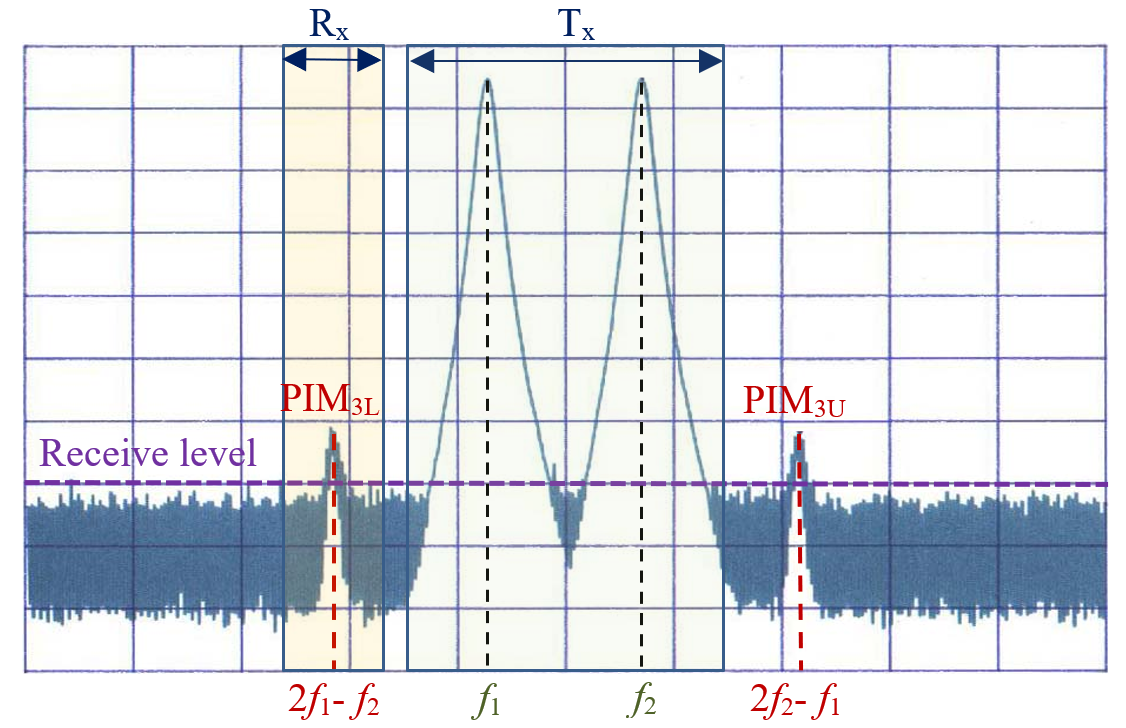
Figure 1. The two high power carriers with frequencies f1 and f2 in the transmit band Tx generate PIM products PIM3L and PIM3U with frequencies 2f1-f2 and 2f2-f1, respectively. The frequency of PIM3L falls in the receive band Rx and causes nonlinear distortions of the received weak information signals.
PIM phenomenology has been studied for more than 50 years but still remains a nagging problem due to its complex multiphysics nature. The basic mechanisms of nonlinearities and PIM generation were explored in metal contacts [22,23,24,25,26,27,28,29], printed RF transmission lines [30,31,32,33,34,35,36], cable assemblies [17,18,31,37,38,39,40], coaxial connectors [41, 42, 43] and antennas [21,44,45,46,47]. The main sources of passive nonlinearities in conductor joints and their interlinks are summarised in Figure 2. They include Metal–Insulator–Metal (MIM) junctions [22,23,24,26,27,28,29], electro-thermal effects [37,40,49,50], surface roughness [32,51,52] and mechanical deformations [52,53,54,55,56]. The electrical contacts with rough surfaces and their RF performance have been recently studied in micro-electro-mechanical systems (MEMS). Whilst the mechanical properties of MEMS have been explored in great detail (see [53,54,55,56] and references therein) the existing models remain limited to the linear devices exposed to weak RF signals. The effects of high RF power on the contacts and junctions of conductors with rough surfaces were studied only in coaxial connectors [38,39,40] and waveguide flanges [57]. But the practical means of mitigating nonlinear distortions and PIM in passive RF circuits remain mostly semi-empirical [10,58].
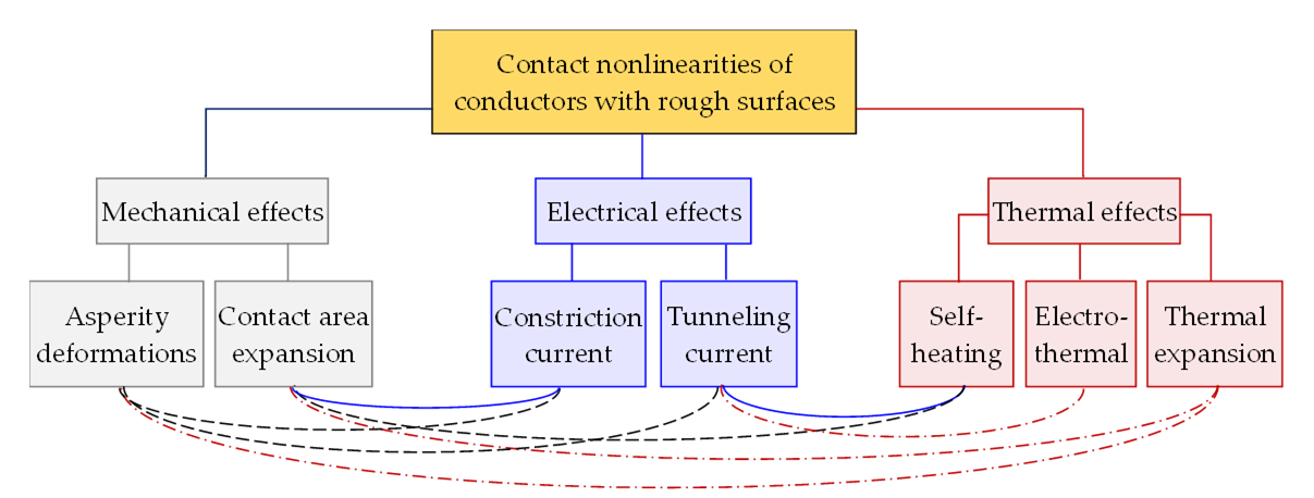
Figure 2. Main types of contact nonlinearities of rough conductor surfaces. Links between different mechanisms of nonlinearities are colour coded in relation to the primary source.
2. Electrical Nonlinearities of Conductor Joints
PIM at contacts of conductors with rough surfaces is a nonlinear multiphysics process with several distinct time scales. The fastest nonlinearities in contacts of good conductors are associated with the electrical effects of charge tunnelling and current constriction at the MIM junctions [17]. The charges are funnelled through the contact spots of rough surfaces as shown in Figure 3(a). The current magnitude depends on the size of a contact area and thickness of an insulating layer that are determined by the applied pressure, local temperature and deformations of the surface asperities. The contact nonlinearities mix and modulate the high-power carriers due to variations of the contact size, temperature and resistance [27,38,39,40]. The thermal effects and mechanical deformations develop much slower than the tunnelling current and the oscillations of the RF carriers. However, both fast and slow nonlinearities remain intrinsically coupled to each other despite their different time scales.
Current flow through the contact asperities of rough surfaces is described by the equivalent circuit shown in Figure 3(b), where Rv1 and Rv2 are the resistances of conductors outside of the asperities. The resistance and capacitance of a pair of compressed or non-touching asperities are represented by Rcm and Ccm. The linear resistance Rcm of the thin oxide film is very high even in contacts of good conductors. For example, Al2O3 film of thickness δs = 1 nm, area 10 μm2 and the macroscopic resistivity ρAl2O3 = 1 × 10¹⁴ Ω·cm has its resistance Rcm = 1014 Ω. Such a high value of Rcm is typical for good insulators and suggests that the charge tunnelling must be responsible for the measured resistance of conductor junctions with thin insulating films. It is also necessary to note that the capacitive reactance 1/jωCcm of the conductor joint can noticeably affect the contact impedance. Indeed, the reactance of this junction is 1/jωCcm = −j89.9 Ω alters the impedance of the contact joint.
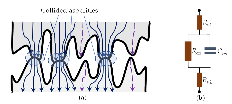
Figure 3. (a) Sketch of contacts between conductors with rough surfaces. Tips of the collided asperities are deformed and the constriction current is funnelled through the contact areas. Only the displacement current (broken lines) is shown at the non-contact asperities. (b) Equivalent circuit of an asperity pair: Rv1 and Rv2 are the resistances of bulk conductors outside asperities; Rcm and Ccm are the resistance and capacitance of either the collided asperities or a pair of isolated asperities.
2.1. Contact and Constriction Resistances
Contacts of conductors with rough surfaces contain the MIM and metal-to-metal junctions. Their resistance depends on the number of touching asperities, size of each contact spot and thickness of an insulating layer in MIM junctions [59]. The mechanical and thermal deformations of individual asperities determine an overall size of the contact area and its contact resistance. The resistance Rc of a contact spot with an equivalent radius a is usually approximated as [60]

where ρc is an average electrical resistivity of a pair of contact asperities, λ is an electron-free path and f(λ/a) is an interpolation function describing a contribution of Maxwell resistance RM = ρc/2a. A good approximation of f(λ/a) proposed in [60] has a maximum error less than 1% at any λ/a

The values of f(λ/a) vary in a relatively narrow range between f(λ/a) ≈ 0.624 at λ >> a and f(λ/a) ≈ 1 at λ << a. The second term in (1) represents Sharvin resistance [61]: that is associated with the collision-free motion of charges. It plays a notable role when the size a of a contact spot is smaller than λ. Then Sharvin resistance RS can exceed Maxwell resistance RM and its contribution to the constriction current becomes significant.
Current constriction by asperities is an inherent feature of the contacts of conductors with rough surfaces [53,57,62]. The constriction resistance is determined by the number of the compressed asperities, sizes of their contact spots and thicknesses of the insulating layer. The constriction current decreases when the size of the contact spot is larger than the mean free path of electrons, a > λ, as evident from (2). Then the charge transport is predominantly diffusive and is dominated by Maxwell resistance RM, defined in (1). In high-quality conductor contacts, e.g., in MEMS, the constriction current is much smaller than the conduction current and is usually combined with the conduction or tunnelling currents [63].
The effective resistance Ru of the whole junction surface containing M asperities can be averaged and approximated as suggested in [53]

where M is the number of compressed asperity pairs, and Rcm is defined by (1) and describes the contact resistance of mth pair of asperities. Thus, Ru is evaluated with (1) where a and ρ are replaced by an effective radius aeff and average resistivity ρav [53]. Such an approximation proved to be fairly accurate when the contact area is large and aeff > λ. Then the contribution of Sharvin resistance is small and deviations of resistivities ρcm from their average value ρav become negligible.
The contact resistances Rcm of individual contact pairs and the whole ensemble, Ru, are the main electrical parameters used for characterising the performance of MEMS switches. They include the effects of both the electrical properties of the contact surfaces and the mechanical deformations. The electro–mechanical models of the contacts in the MEMS switches have been discussed in detail in [53,54,55,63].
2.2. Nonlinearity of MIM Contacts
The tunnelling current in MIM contacts subjected to RF power is the main source of their fast nonlinearity [22,23,24]. When a thin insulating film of a few nanometre thick separates asperities of rough conductors, the tunnelling current flows through. An efficient interaction of the high-power RF carriers with free charges is the result of the small timescale of the tunnelling effects in the conductor junctions. However, when the thickness of the insulating layer is commensurate with the free path of electrons, charges cannot penetrate the potential barrier. The tunnelling current rapidly decays and becomes practically negligible as the insulator between asperities is thicker than 5-10 nm.
In the widely accepted Simmons model, the current density J(Vg) in MIM junction is represented as

2.3. The Effect of Surface Roughness
Surface roughness significantly affects the performance of electrical contacts in high frequency applications [52,53,54,55,57]. The statistical models have been used for simulating the contacts of rough surfaces. Gaussian distribution of contact asperity heights with the standard deviation up to 20% from an average value was examined in [64], taking into account the effect of an insulator thickness on the contact resistance of rough surfaces. Using the Brinkman–Dynes–Rowell model [65], it has been shown that a single thickness model reasonably estimates the surface conductance when the standard deviation of asperity heights remains within 5% of the average value.
2.4. Thermionic Emission
Thermionic emission is the process of electron discharge from the free metal surface. In good conductors, it occurs at very high temperatures, above 1000°C [66], when hot electrons can gain enough energy to break their bonding and escape from the conductor surface.
At operational temperatures of electronic devices, the thermionic emission current in joints of good conductors is practically negligible. It also decreases exponentially with the thickness of the insulating layer and becomes undetectable as the insulator layer is thicker than 5 nm. Thus, the thermionic emission current can be neglected in contacts of good conductors.
3. Thermal Nonlinearities at Contacts of Good Conductors
3.1. Self-Heating Effect and Nonlinearity of Contact Resistivity
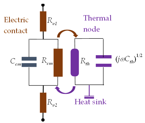
Heat generation is an inherent feature of electromagnetic (EM) wave interactions with conductors and their contact joints. This multiphysics process couples the electric and thermal domains as illustrated in Figure 4. Namely, the dissipative losses of high-power RF signals generate heat which, in turn, alters the resistance of conductors and causes their thermal expansion and mechanical deformations. These nonlinear effects are interlinked despite the time scales of the thermal and mechanical processes notably differ.
3.2. Electro-Thermal Effect in Contact Joints and PIM Generation
Electrothermal PIM (ET–PIM) is caused by self-heating due to conductor and dielectric losses [37]. ET–PIM has a distinct signature of the nonlinear coupling of electrical and thermal domains as illustrated in Figure 4. The basic mechanism of this nonlinearity is the thermal modulation of resistivity. In essence, the heat due to RF losses alters the resistance of a conductor, which is heated by the high-power carriers, and this results in the generation of PIM products. The effects of ET–PIM have been studied in the termination resistors [37,50], printed transmission lines [36,68] and thin-film coplanar waveguides with spatially inhomogeneous current distributions [35]. The developed theory of the ET–PIM and supporting experiments [36,37,68] have revealed that the baseband resistivity of conductors is modulated by the heat oscillations. The effect of resistivity variation on the skin depth due to modulation of the RF carriers was analysed in [45,46]. These studies have enabled the development of the qualitative analytical model, which sheds light on the principal mechanisms of ET–PIM generation and provides an accurate assessment of signal distortion by ET–PIM in the full-wave EM simulations [33,34,35,36,68].
Evaluations of the dissipative losses and the rate of self-heating are the critical steps in the ET–PIM analysis. While the skin effect is routinely accounted for in the EM simulations when calculating the losses of imperfect conductors, surface roughness is normally ignored despite its proven major impact on the performance of printed circuits [51,52] and MEMS switches [53,54,55].
3.3. Thermal Expansion of the Contact Area
The heat, generated by the high RF power, is dissipated in conductors and their joints and causes the thermal expansion and deformation of contact surfaces. As the result, the contact areas and the conductor resistivity ρc(x) increase with temperature. The contact resistance Rcm of asperities also grows with temperature, whilst the pace of its growth depends on the relation between the temperature coefficient of resistivity α, the rate of the thermal expansion of the contact areas and asperity deformations. These thermal effects cause nonlinearity of the contact resistance that inflict nonlinear signal distortions.
4. Mechanical Nonlinearities at Conductor Contacts
4.1. Effect of Asperity Deformations on Conductor Resistivity
Contact resistances of rough surfaces calculated with the aid of (1) or (3) account for the effects of external pressure and deformations of the compressed asperities [53,54,55,56,57,63,69]. The factors affecting the contact area expansion and asperity compression include mechanical stresses, elasticity and surface finish. At low pressure, the colliding asperities experience elastic deformations and their contact areas enlarge. When contact pressure increases, the compressed asperities experience plastic deformations and their contact regions are hardened. This results in the slowing down of the expansion of the contact spots and a change in contact resistivity ρc(x) [53,59,63]. The combined effect of the contact area enlargement and asperity hardening is governed by the relations between the contact pressure and contact resistance. These nonlinear effects of strain hardening and softening on the resistivity ρ(x) of a contact spot is accounted in [70]

where ρc(x) is the temperature dependent resistivity of a contact, εp is plastic strain, εref is a reference strain, q is a material dependent parameter, Q is the activation energy for the mechanism of relaxing the stored dislocations, T is the absolute temperature and Boltzmann constant k = 1.38 × 10⁻²³ J/K.
In addition to altering the contact resistance, heat softens contact asperities [53,54,55,56] and increases their plastic and creep deformations.
4.2. Contact Area Expansion
Pressure, applied to the contacts of conductors with rough surfaces, causes asperity deformations. The compressed asperities expand laterally, and their contact areas increase with the applied pressure and mechanical stress, depending on the material stiffness and surface coatings. When exposed to the RF power, the contact spots are heated due to conductors’ dissipation losses but the compressed asperities spread gradually to reduce their strain. The thermal expansion and softening of the contact spots also cause plastic deformations and creep of the colliding asperities. These effects were examined in RF MEMS with frustoconical contact asperities [69]. At a small radius r1 of the undeformed frustum tip, contact radius rc(t) of the compressed asperity changes with time t as approximated in [69]

where L is asperity initial height, C is a constant dependent on the contact material and creep mechanism, q is a slant angle of the asperity frustum, F is contact load, Qc is the activation energy for creep, α = 1/(1 + 2p), and p is the stress exponent that varies between 3 and 10, depending on the material composition. The value of α is specifically related to the creep coefficient, and it is normally fitted to the experimental data. Values of α are usually small, and in the example presented in [69] α < 0.1.
5. Conclusions
The main physical sources of passive nonlinearities in contact joints can be broadly cast in the three main groups of (i) electrical, (ii) thermal and (iii) mechanical effects. It is shown that these mechanisms are intrinsically linked but their time scales differ significantly. Namely, the electromagnetic interactions at MIM junctions are very fast and follow the pace of the RF signals. The thermal processes are much slower being limited by the speed of heat flow in the conductor contacts. The effects of the mechanical deformations are even slower. Roughness of the contact surfaces considerably increases losses and nonlinearity in contact joints, especially at RF frequencies. The main sources of the passive nonlinearities at the contacts of rough surfaces are discussed and illustrated here by the examples of good conductors.
An important conclusion is that the electrical, thermal and mechanical contact nonlinearities are linked intrinsically despite their very different types and time scales. Namely, the MIM nonlinearity is of the exponential type, whereas the electrothermal nonlinearity is of Kerr type. The nonlinearities of mechanical deformations are of the mixed type described by the combination of the exponential and algebraic dependencies. Therefore, the analysis of PIM in contact joints of good conductors requires multiscale multiphysics models taking into account several distinct types of nonlinearities involved.
The main multiphysics mechanisms of passive intermodulation (PIM) in contact joints of good conductors are discussed in more detail in [71].Rc=ρc2a[f(λa)+8λ3πa]
This entry is adapted from the peer-reviewed paper 10.3390/electronicmat3010007