Your browser does not fully support modern features. Please upgrade for a smoother experience.
Please note this is an old version of this entry, which may differ significantly from the current revision.
GeSn materials have attracted considerable attention for their tunable band structures and high carrier mobilities, which serve well for future photonic and electronic applications.
- GeSn growth
- selective etch
- strain modulation
- RPCVD
1. Introduction
GeSn has aroused extensive attention as a result of its direct bandgap properties [1], compatibility with Si CMOS processes [2,3,4,5,6], higher absorption coefficients at short-wavelength infrared (SWIR) windows [7], and higher carrier mobilities compared with Si and Ge, etc. [3]. These characteristics show that GeSn materials will be promising for both optoelectronics and high-speed electronics for silicon photonic-electronic platforms in the near future. It is also expected that GeSn could open applications for thermoelectric materials in the near future [8,9]. There are several challenges in growing high quality GeSn: (I) the lattice mismatch between Ge and Sn is 14.7% and is even higher at 17% between Sn and Si; (II) incorporation of Sn in Ge is difficult due to the low solubility (<1%) of Sn in Ge and the instability of α-Sn above 13 °C; and (III) Sn precipitation and Sn agglomeration occur during growth. Therefore, growth tools, such as molecular beam epitaxy (MBE) [10,11,12], reduced pressure chemical vapor deposition (RPCVD) [13,14,15,16,17,18,19,20,21,22], ultra vacuum chemical vapor deposition (UHVCVD) [23], physical vapor deposition (PVD) [24], and sputtering technique [25,26] have been proposed to grow GeSn at low temperatures. Compared to MBE and PVD, CVD has the advantages of lower costs, higher growth rates, larger wafer sizes, and mass production potential which can easily be transferred to the Si-based microelectronic and photonic industry. As early as 2001, Kouvetakis’s group from Arizona State University (ASU) grew GeSn and GeSnSi via reactions of Si–Ge hydrides and SnD4 in a UHVCVD chamber, but SnD4 molecules are very unstable [27,28]. Then, in 2011, researchers from IMEC [14] and KTH proposed the growth of GeSn using commercially available reaction precursors (SnCl4/Ge2H6) in a production RPCVD tool [18]. Since then, many research groups reported the growth of GeSn using precursor combinations of SnCl4/Ge2H6 and SnCl4/GeH4 [13,14,15,16,17,18,19,20,21,22,23]. Moreover, GeSnSiC alloys were also grown using Si2H6, Ge2H6, SnCl4, and SiCH6, precursors which are also important for photonic applications [19,20]. From the mass production perspective, GeH4 is preferred to Ge2H6, owing to its wider usage and lower cost. In order to improve material properties, the effects of growth temperature, growth pressure, carrier gas, strain relaxation, and doping on GeSn growth were systematically investigated. Experimental results indicate that growth temperature, growth pressure, and strain relaxation were major factors towards achieving high Sn composition and high quality GeSn [29,30].
. Growth Kinetics
The fundamental problem with growing GeSn layers is segregation of Sn atoms. There are two main factors which govern Sn segregation: chemical and size effects. The first effect depends on the heats of sublimation of Sn (65 kcal/mole) and Ge (89 kcal/mole), which in fact determine whether Sn-to-Sn or Sn-to-Ge bonding is favored. The size effect originates from the size difference between Sn and Ge atoms. Therefore, we may conclude that high incorporation of Sn in Ge is a real challenge as a result of both aforementioned effects.
Prior to GeSn growth, a Ge buffer with a thickness of at least 1000 nm is necessary to be deposited for high quality epitaxy. The Ge buffer layer contains two layers which are grown at a temperature of 450 °C for the low layer, and at 650 °C for the cap layer. The first layer is highly defective; meanwhile, the second layer has significantly higher epitaxial quality. An annealing treatment at 850 °C ensures the defect density is minimized to a level of 107 cm−2. Since the main goal of this study is to incorporate high Sn content in Ge, the quality of the buffer layer is very important. Figure 3 illustrates the series of grown samples in this study. The amount of SnCl4 introduced into the epi chamber was increased in three steps of 0.8, 1, and 1.5 g/h. In these samples, Sn segregation appears as Sn dots on the surface of the GeSn layer. The sizes of the Sn dots depend on the thickness of the GeSn layer, and they become larger for thicker GeSn layers. Therefore, it is important in the characterization of GeSn layers that the presence of Sn dots not be misjudged as surface roughness, especially when they are small for thin GeSn layers. Since Sn atoms are large, and since the heat of sublimation for Sn is less than that for Ge, segregation of Sn in Ge buffer occurs from both chemical and size effects.
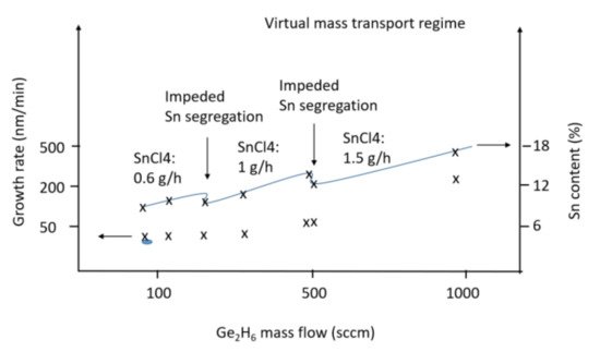
Figure 3. Growth parameters of GeSn deposition and its related Sn contents.
In general, the growth of Si-based materials using CVD follows two regimes: kinetic and mass transport. In kinetic mode, the growth rate is temperature-dependent, whereas in mass transport mode the growth rate is dependent on reactant gas partial pressures. In this study, GeSn growth occurs at 280–310 °C; then, it is expected that epitaxy follows the kinetic mode. As we know, Sn segregation depends strongly on the introduced Sn content; meanwhile, Figure 3 illustrates that Sn segregation is decreased by increasing the Ge partial pressure, and diminishes when Ge partial pressure reaches a critical value. Surprisingly, the growth rate is also increased by increasing the Ge partial pressure. By applying high Ge partial pressure, the number of Ge atoms is increased, resulting in a dramatic change to the kinetics of atoms where lateral diffusion of atoms becomes limited. We believe Sn segregation is decreased as a result of the high growth rate and limited lateral diffusion of Sn atoms. This condition of growth could be called virtual mass transport mode at low temperature growth. Reaching this point is the key issue for significant corporation of Sn into a Ge crystal matrix to occur. In the next step, by introducing more Sn atoms, a new condition is reached and it becomes necessary to deal with the excess of Sn atoms during GeSn growth; therefore, Ge atoms will be needed to decrease segregation. By stepwise introduction of more Sn atoms, the Ge partial pressure must be increased with each new step. In Figure 3, three points reflect the optimized growth parameters. As a result of this stepwise approach, 18% of Sn could be incorporated in Ge.
In order to examine the quality of the GeSn layers, high-resolution X-ray diffraction (HRXRD) including reciprocal lattice maps were performed, as shown in Figure 4. The rocking curves illustrate thickness fringes, indicating high interfacial quality. Layer quality is often estimated using the full-width half-maximum (FWHM) method, but in these samples the strain relaxation was not the same due to different layer thicknesses. Therefore, HRRLM was performed, as shown in Figure 4b, to determine strain in both vertical and lateral growth directions. In this way, the strain relaxation could be measured and discussed. HRRLM was performed around (2 2 4) reflection, which is most sensitive to the defects. This is due to the low incident angle of the X-ray beam at 8.7° which makes a long propagation of the X-ray beam along the GeSn layer, and easily reveals the defects [52]. The positions of GeSn and Ge peaks in the reciprocal lattice were determined, then the mismatch parameters were calculated. In the HRRLMs, the shape of the GeSn peak and the diffused scattering provide information about the presence of Sn dots within the GeSn layer. In these maps, the GeSn peak is aligned with the Ge peak along the (001) direction showing minor strain relaxation. The GeSn peak shifts out but is still along the (001) direction, illustrating the increase in strain in the epilayers.
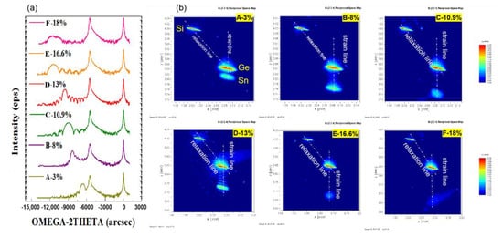
Figure 4. X-ray analysis of GeSn/Ge layers (a) rocking curves and (b) 224 HRRLMs.
3. Strain Modulation of GeSnOI by Vertical Etching
The strain modulation of GeSnOI was studied by stepwise etching the Ge buffer. Figure 10 shows HRXRD results of as-grown and after 20 s, 100 s, and 120 s etching times of GeSnOI. In these experiments, the intensity of the Ge peak decreases gradually with increases in etching time, and later appears as Ge is completely etched away.
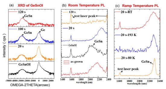
Figure 10. (a) XRD of GeSnOI as-grown (black line) and after wet etchings of 20 s (orange line), 100 s (blue line), and 120 s (red line); (b) PL at room temperature of GeSn as-grown (red line), GeSnOI (black line), and after wet etchings of 20 s (blue line), 100 s (amaranth line), and 120 s (orange line); and (c) PL of GeSnOI after wet etching of 20 s at temperatures of 80 K (orange line), 193 K (blue line), and room temperature (red line).
Figure 10b shows the GeSn peak has a blue-shift after the bonding process. It is believed that this shift is a result of the annealing treatment (300 °C 1 h) which could cause a number of Sn atoms to be pushed out from substitutional sites, resulting in strain reduction. This explanation originates from the fact that we observed no defects in HRTEM results. Meanwhile, the etching of the Ge buffer creates a red-shift, as expected. The red-shift is caused by stress release and bandgap alignment in GeSn. Table 4 and Figure 10c demonstrate more PL investigation on the GeSnOI sample with a 20-s etching of Ge buffer at different temperatures. The PL peak’s FWHM at room temperature (shown as Table 4) is decreased at low temperature analysis, which is consistent with freezing of imperfections in the epilayer.
Table 4. PL data for the GeSn peak at 80 K and at room temperature (RT) after Ge vertical wet etching.
| Sample | FWHM-80 K/nm | Peak of GeSn-80 K/nm | FWHM-RT/nm | Peak of GeSn-RT/nm |
|---|---|---|---|---|
| GeSn Before bonding | -- | -- | 251 | 2166 |
| GeSnOI | 129 | 2040 | 134 | 2039 |
| 20 s | 60 | 2286 | 284 | 2270 |
| 120 s | 26 | 2279 | 345 | 2232 |
In order to find out the strain distribution in the above sample GeSnOI, NBD analysis was performed, as shown in Figure 11a–c, and more details about estimated strain values are demonstrated in Table 5. The strain is distributed at the top level in the middle of the GeSn layer and more relaxation occurs in the vertical direction close to the Ge buffer. No defects are created in GeSn layers, and by removing more Ge buffer the strain is constantly decreased.
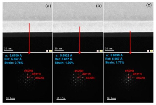
Figure 11. NBD in different GeSn regions of sample wet etched for 20 s; the reference is bulk Ge with lattice constant 5.657 Å. (a) Up; (b) middle; (c) down.
Table 5. NBD results about GeSnOI strain before etching, and after wet etching for 20 s and 120 s.
| Sample | Bulk Strain | Strain⊥(002) | Strain//(220) |
|---|---|---|---|
| GeSnOI | 2.79% | 2.11% | 0.47% |
| 20 s | 1.90% | 1.60 % | 0.17 % |
| 120 s | 1.19% | 2.24% | −0.32% |
This entry is adapted from the peer-reviewed paper 10.3390/nano12060981
This entry is offline, you can click here to edit this entry!