Graphitic nanocup architectures are low aspect ratio hollow graphitic nanostructure that can be precisely controlled and modified for various applications.
- graphitic nanoscale architecture
- precisely controllable nanostructure
- flexible and transparent electrodes
- carbon nanocup container
The synthesis of controllable hollow graphitic architectures can engender revolutionary changes in nanotechnology. Here, authors present the synthesis, processing, and possible applications of low aspect ratio hollow graphitic nanoscale architectures that can be precisely engineered into morphologies of (1) continuous carbon nanocups, (2) branched carbon nanocups, and (3) carbon nanotubes–carbon nanocups hybrid films.
1. Introduction
For decades, diverse graphitic nanostructures (e.g., nanographite, carbon nanotubes, carbyne, and graphene) have been actively researched for applications in energy storage devices, bio/chemical sensors, drug delivery, etc. [1][2][3][4][5][6][7][8][9][10][11][12][13][14]. While significant progress has been made on both developing large-scale synthesis and unveiling their exceptional properties, there remain challenges in controlling morphology and proportion of individual nanoscale units, which limits their use in down-to-earth applications[15][16][17][18][19][20][21][22]. Particularly one-dimensional (1-D) graphitic structures (e.g., carbon nanotubes) are attractive in that other nanomaterials or functional molecules can be trapped or embedded inside them for advanced multicomponent systems[23][24][25]. However, it is difficult to effectively intercalate abundant nanomaterials such as nanoparticles, drugs, or polymers within the hollow tubular structure where length/diameter (L/D) aspect ratios often range between 103 and 105[25][26]. Fortunately, the recent flurry of activity successfully introduced a unique cup-shaped carbon nanostructure that allows unprecedented control over structural morphology and dimension and easy insertion of nanomaterials inside them[27]. This review covers the synthesis and processing of hollow carbon nanostructures and demonstrations of their potential applications. This hollow carbon nanostructured film was fabricated by precisely tailoring the nanopores of the anodized aluminum oxide (AAO) template, which has been widely used to form a dense array of nanochannels[28][29][30][31][32][33][34][35]. The AAO template allows precise control of nanoscale pores such as the length, width, and diameter [21][27][36][37][38][39][40][41][42], enabling the design of cup-shaped nanostructures with low aspect ratio. By depositing carbon materials on this AAO template, low aspect ratio graphitic nanoscale cup structures can be fabricated, resulting in a film of uniformly arranged carbon nanocups (see Figure 1). The deposition of the graphitic carbon film is performed by a high-temperature chemical vapor deposition (CVD) process, and the thickness of the nanocups film could be controlled by changing the CVD reaction time. The unique carbon nanostructured cups are continuously and uniformly connected like a thin film of honeycombs. The film of connected nanocups exhibits high specific surface area and enables fast electron transfer [43][44]. Furthermore, it is mechanically flexible and optically transparent. Shape control is not only limited to the dimensions but also in terms of fabricating branches on the bottom of the nanocups or growing vertically aligned CNTs inside the cups by employing a thermal CVD process. This connected nanocups film is an ideal template to build a multicomponent system, as other nanomaterials, molecules, or polymers can be easily inserted and evenly distributed over the cups[27],[36][37][38][45][46].
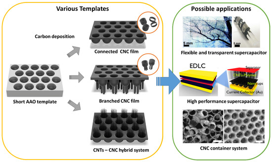
Figure 1. Schematic of various architectures using the anodized aluminum oxide (AAO) template and their applications: flexible and transparent supercapacitors[37], high-performance supercapacitors[36], and carbon nanocups (CNC) container system[27]. Insert images were reproduced with permission from[27][36][37]. Copyright (2009) American Chemical Society, (2012) American Chemical Society, and (2012) Springer Nature.
Figure 1 shows a schematic of various carbon nanocups (CNC) architectures and their potential applications. CNC diameter and length can be controlled to optimize the function of the CNC film. We review three CNC-based nanostructures: (1) thin CNC film, (2) branched CNC film, and (3) CNTs–CNC hybrid structure. These structures are useful for applications that require optical transparency, mechanical flexibility, and structural continuity. In this paper, we cover (1) flexible and transparent supercapacitors, (2) high-performance supercapacitors, and (3) CNC container system that can accommodate nanoparticles, polymers, or liquid droplets.
2. Fabrication and Modification of Graphitic Nanoscale Architectures
2.1. Carbon Nanocups (CNC) Thin Film
Carbon nanocups (CNC) thin film is an array of carbon nanocups with a short aspect ratio of 1–2 (Figure 2a,b). This two-dimensional film contains a well-organized array of nanocups where the uniform density results in high porosity. The structure of the nanocups can be precisely controlled in terms of their length, diameter, and wall thickness. Figure 2c shows the scanning electron microscopy (SEM) image of a CNC film with an L/D aspect ratio of 2, which has a 100 nm diameter and 200 nm length. Figure 2d shows the shorter CNCs with an aspect ratio of 1 with 80 nm diameter and 80 nm length. The thickness of nanocups shown in Figure 2 is 10 nm, and can be easily controlled by the time of carbon deposition or the concentration of carbon source. The CNC film demonstrates attractive features such as ease of structure control, high porosity, excellent flexibility, and high mechanical strength[27][37].
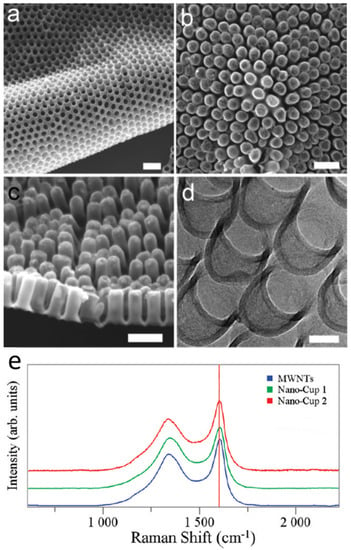
Figure 2. SEM and TEM micrographs of a two-dimensional carbon nanocup film structure after removing the AAO template. SEM images show (a) the upside of highly dense carbon nanocup arrays connected with a thin graphite layer, (b) a two-dimensional and flexible film of carbon nanocups, and (c) the side view of carbon nanocups (100 nm diameter and 200 nm length) connected with a graphitic layer of 10 nm thicknesses. Scale bars are 200 nm. (d) A TEM image shows connected arrays of carbon nanocup film with 80 nm diameter and 80 nm length. Scale bar is 50 nm. (e) Raman spectra taken from MWNTs (10 μm in length), long nanocups (180 μm in length), and short nanocups (60 nm in length). Reproduced with permission from[27]. Copyright (2009) American Chemical Society.
The CNC film is fabricated using the AAO template that was fabricated by a two-step anodization process. A high-purity Al foil (Alfa Aesar, 99.99%) was first anodized at 40–45 V for 4 h in 3–5% oxalic acid (C2H4O2) solution at room temperature. Then, the anodized film was dipped into an acid mixture solution (5% of phosphoric and 5% of chromic acid) for 24 h. After the removal of the first anodized aluminum layer, the second anodization, which plays a crucial role in controlling the dimension of CNC, was performed. To fabricate the shorter aspect ratio CNC, the second anodization was performed for extremely short time of 20–40 s, and this resulted in 80–200 nm of length. After that, the sample was soaked into the phosphoric acid again for 1 h to widen the diameter of the nanochannel. After the preparation of a well-controlled AAO template, the carbon was deposited on the template by a chemical vapor deposition (CVD) using acetylene as a carbon source. After the deposition of the graphitic carbon layer on the AAO template, the sample was soaked in 33% of the hydrofluoric acid solution to remove the AAO template. Finally, a self-standing and flexible thin CNC film was achieved.
Raman spectroscopy was performed using a 532 nm laser probe to investigate the lattice structure and graphitization of the nanocup structure. The disorder-induced D band is an indicator of presence of defects while the G band (~1600 cm−1) is associated with the tangential modes of the graphene structure. The D and G bands have been observed in the spectral range of 1200–1700 cm−1 [47][48]. Figure 2e shows the Raman spectra obtained from multiwalled carbon nanotubes (MWNTs) with 10 μm length and nanocups of similar diameter that have different lengths of 180 μm (nanocup 1) and 60 nm (nanocup 2). We have observed that the peak intensity ratios (ID/IG) are about 0.41 and 0.45 for long and short CNCs, respectively, comparable to that of long MWNTs (10 μm in length, ID/IG=~0.32). This result indicates that the degree of disorder of the carbon nanocup structures is comparable to that of MWNTs.
2.2. Branched Carbon Nanocups (B-CNC) Thin Film
Figure 3 shows SEM images of CNCs (3a−c) and branched CNCs (3d−f). To fabricate branched CNCs, CNCs were first fabricated with channels of 80 ± 10 nm in diameter and 140 ± 10 nm in length. Afterwards, branches were developed at the bottom of the nanocups with 25 nm in diameter and 330 ± 10 nm in length. Such branched CNCs maximize the surface area of the thin film, and this highly dense and ordered array of nanocups with continuous graphitic thin film can be an ideal electrode material for energy storage devices. This branched CNC thin film shows attractive features such as excellent flexibility and strong mechanical strength, precisely controllable structure, and even improved porosity with a large surface area.
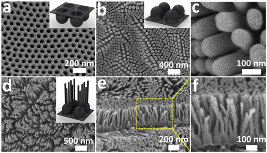
Figure 3. SEM images of CNC. SEM images of (a) concave and (b,c) convex, and (d–f) branched nanocup films. (b) SEM image of convex nanocup film with 80 ± 10 nm in diameter and 140 ± 10 nm in length, and (c) shows a high magnification of (b). (e,f) Cross-sectional views of (d) branched nanocup film, and (f) is a high magnification image of (e), where short carbon nanotubes (25 nm in diameter and 330 ± 10 nm in length) are branched from the bottom of a nanocup. The inset figures, respectively, show schematics of concave, convex, and branched convex nanocup film. Reproduced with permission from[37]. Copyright (2012) Springer Nature.
The fabrication of branches on the bottom of CNC follows the same procedure as CNC film fabrication. After an hour of widening process, a third anodization is carried out for 5 min at 25 V in a 3% oxalic acid solution. The graphitic carbon deposition by CVD using acetylene was then followed, resulting in the production of a continuous film of branched nanocups. The surface area of the branched CNC film was calculated as 63 m2/g, while CNC film (convex type) showed surface area of 49 m2/g. When this branched CNC film was used as an electrode, the surface area exposed to the electrolyte was 2.3 times higher than the typical convex CNC film. Further, this film showed excellent electrical conductivity of 117 S/m, which is higher than the regular activated carbon electrode[49].
2.3. Carbon Nanotubes (CNTs)–CNC Hybrid Structure
The hybrid structure of CNTs and CNCs was developed to increase the surface area to be even greater than the branched CNC film. The vertically aligned CNTs were grown on the CNC by two steps of the CVD process. Figure 4a shows SEM images of the well-organized and interconnected CNCs with low aspect ratio, and Figure 4b shows CNTs–CNC hybrid structure. CNC film was prepared by AAO nanochannels and catalyst-free CVD process. To fabricate CNTs–CNC hybrid structure, 1.5 nm of iron was deposited on the surface of the prepared CNC layer as a catalyst for CNTs growth. Then, vertically aligned CNTs were grown by a water-assisted CVD technique[50][51]. The water-assisted CVD process did not exceed 650 °C to avoid melting of AAO template. This second CVD process resulted in highly dense vertically aligned CNTs with 5–10 μm of length on the porous CNC structure (Figure 4b).
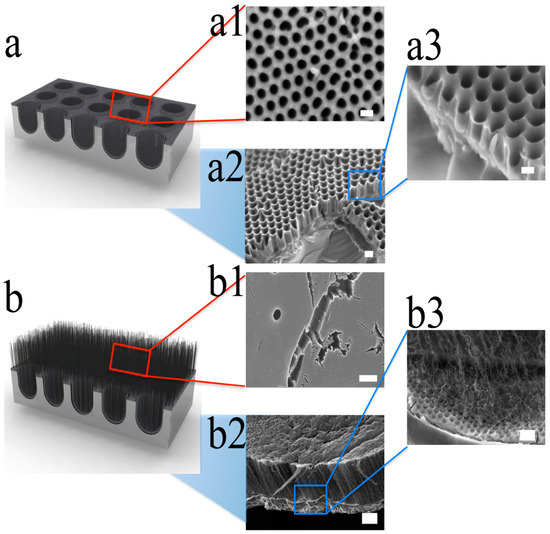
Figure 4. Schematic drawing of SEM images from CNCs and CNTs−CNC hybrid structure. (a) Schematic illustration of CNC. (a1) SEM image on the top surface of CNC, (a2) a low-magnification SEM of the cross-sectional view, and (a3) high-magnification cross-sectional images. The scale bars are 200, 200, and 120 nm, respectively. The images clearly show hollow structures with low aspect ratio. (b) Schematic of vertically aligned CNTs grown on the surface of CNC. (b1) A top-view SEM image of vertically aligned CNTs, (b2) a side view of low-magnification SEM image, and (b3) high-magnification SEM image of a vertically aligned CNTs−CNC structure. The scale bars are 200, 4, and 400 nm, respectively. Reproduced with permission from[36]. Copyright (2012) American Chemical Society.
The specific surface area of CNC arrays was measured by surface adsorption analysis using the Brunauer–Emmett–Teller (BET) theory, and it was 810 m2/g. The high porous CNC film showed larger specific surface area than the experimentally synthesized CNTs (700–790 m2/g)[52][53]. The CNC film itself had high specific surface area, but the CNTs–CNC hybrid structure showed even higher specific surface area of 1340 m2/g. The increased surface area of the CNTs–CNC hybrid structure indicated that vertically oriented CNT walls provide surface exuberance towards the nanocups. The CNTs–CNC hybrid structure provides higher surface area than CNTs itself[36][52] and has a continuous CNC film on the bottom that increases electrical conductivity.
This entry is adapted from the peer-reviewed paper 10.3390/nano10091862
References
- Bendjemil, B.; Cleymand, F.; Pichler, T.; Knupfer, M.; Fink, J. Carbon Nanostructures in Cancer Diagnosis and Therapy. J. Nanom. Nanos Tech. JNNT-110 2019, 2019, 1–18. [Google Scholar]
- Bezzon, V.D.; Montanheiro, T.L.; de Menezes, B.R.; Ribas, R.G.; Righetti, V.A.; Rodrigues, K.F.; Thim, G.P. Carbon Nanostructure-based Sensors: A Brief Review on Recent Advances. Adv. Mater. Sci. Eng. 2019, 2019, 4293073. [Google Scholar] [CrossRef]
- Chu, J.O.; Dimitrakopoulos, C.D.; Grill, A.; McArdle, T.J.; Pfeiffer, D.; Saenger, K.L.; Wisnieff, R.L. Carbon Nanostructure Device Fabrication Utilizing Protect Layers. U.S. Patent 9,768,288, 19 September 2017. [Google Scholar]
- Iglesias, D.; Bosi, S.; Melchionna, M.; Da Ros, T.; Marchesan, S. The glitter of carbon nanostructures in hybrid/composite hydrogels for medicinal use. Curr. Top. Med. Chem. 2016, 16, 1976–1989. [Google Scholar] [CrossRef] [PubMed]
- Kaur, J.; Gill, G.S.; Jeet, K. Applications of carbon nanotubes in drug delivery: A comprehensive review. In Characterization and Biology of Nanomaterials for Drug Delivery; Elsevier: Amsterdam, The Netherlands, 2019; pp. 113–135. [Google Scholar]
- Kim, H.; Gao, S.; Hong, S.; Lee, P.-C.; Kim, Y.L.; Ha, J.U.; Jeoung, S.K.; Jung, Y.J. Multifunctional primer film made from percolation enhanced CNT/Epoxy nanocomposite and ultrathin CNT network. Compos. Part B Eng. 2019, 175, 107107. [Google Scholar] [CrossRef]
- Hong, S.; Kim, H.; Gao, S.; Lavall, R.L.; Jung, H.Y.; Jung, Y.J. Reconfigurable solid-state electrolytes for high performance flexible supercapacitor. J. Power Sources 2019, 432, 16–23. [Google Scholar] [CrossRef]
- Lamy-Mendes, A.; Silva, R.F.; Durães, L. Advances in carbon nanostructure–silica aerogel composites: A review. J. Mater. Chem. A 2018, 6, 1340–1369. [Google Scholar] [CrossRef]
- Liu, H.; Zhang, L.; Yan, M.; Yu, J. Carbon nanostructures in biology and medicine. J. Mater. Chem. B 2017, 5, 6437–6450. [Google Scholar] [CrossRef]
- Mondal, K.; Balasubramaniam, B.; Gupta, A.; Lahcen, A.A.; Kwiatkowski, M. Carbon Nanostructures for Energy and Sensing Applications. J. Nanotechnol. 2019, 2019, 1454327. [Google Scholar] [CrossRef]
- Piovesana, S.; Iglesias, D.; Melle-Franco, M.; Kralj, S.; Cavaliere, C.; Melchionna, M.; Laganà, A.; Capriotti, A.L.; Marchesan, S. Carbon nanostructure morphology templates nanocomposites for phosphoproteomics. Nano Res. 2020, 13, 380–388. [Google Scholar] [CrossRef]
- Xiong, G.; He, P.; Lyu, Z.; Chen, T.; Huang, B.; Chen, L.; Fisher, T.S. Bioinspired leaves-on-branchlet hybrid carbon nanostructure for supercapacitors. Nat. Commun. 2018, 9, 790. [Google Scholar] [CrossRef]
- Yu, L.; Hu, H.; Wu, H.B.; Lou, X.W. Complex hollow nanostructures: Synthesis and energy-related applications. Adv. Mater. 2017, 29, 1604563. [Google Scholar] [CrossRef] [PubMed]
- Gao, S.; Jiang, Q.; Shi, Y.; Kim, H.; Busnaina, A.; Jung, H.Y.; Jung, Y.J. High-performance lithium battery driven by hybrid lithium storage mechanism in 3D architectured carbonized eggshell membrane anode. Carbon 2020, 166, 26–35. [Google Scholar] [CrossRef]
- Liu, J.; Rinzler, A.G.; Dai, H.; Hafner, J.H.; Bradley, R.K.; Boul, P.J.; Lu, A.; Iverson, T.; Shelimov, K.; Huffman, C.B. Fullerene pipes. Science 1998, 280, 1253–1256. [Google Scholar] [CrossRef] [PubMed]
- Lu, K.; Lago, R.; Chen, Y.; Green, M.H.; Harris, P.F. Mechanical damage of carbon nanotubes by ultrasound. Carbon 1996, 34, 814–816. [Google Scholar] [CrossRef]
- Shelimov, K.B.; Esenaliev, R.O.; Rinzler, A.G.; Huffman, C.B.; Smalley, R.E. Purification of single-wall carbon nanotubes by ultrasonically assisted filtration. Chem. Phys. Lett. 1998, 282, 429–434. [Google Scholar] [CrossRef]
- Venema, L.C.; Wildöer, J.; Tuinstra, H.T.; Dekker, C.; Rinzler, A.; Smalley, R. Length control of individual carbon nanotubes by nanostructuring with a scanning tunneling microscope. Appl. Phys. Lett. 1997, 71, 2629–2631. [Google Scholar] [CrossRef]
- Gu, Q.; Gao, Z.; Zhao, H.; Lou, Z.; Liao, Y.; Xue, C. Temperature-controlled morphology evolution of graphitic carbon nitride nanostructures and their photocatalytic activities under visible light. Rsc Adv. 2015, 5, 49317–49325. [Google Scholar] [CrossRef]
- Subramanian, S.; Purdy, G. Graphite morphology control in cast iron. In Proceedings of the F. Weinberg International Symposium on Solidification Processing, Hamilton, ON, Canada, 27–29 August 1990; pp. 289–303. [Google Scholar]
- Xia, Y.; Yang, Z.; Mokaya, R. Simultaneous control of morphology and porosity in nanoporous carbon: Graphitic mesoporous carbon nanorods and nanotubules with tunable pore size. Chem. Mater. 2006, 18, 140–148. [Google Scholar] [CrossRef]
- Zhou, B.-X.; Ding, S.-S.; Zhang, B.-J.; Xu, L.; Chen, R.-S.; Luo, L.; Huang, W.-Q.; Xie, Z.; Pan, A.; Huang, G.-F. Dimensional transformation and morphological control of graphitic carbon nitride from water-based supramolecular assembly for photocatalytic hydrogen evolution: From 3D to 2D and 1D nanostructures. Appl. Catal. B Environ. 2019, 254, 321–328. [Google Scholar] [CrossRef]
- Liu, Y.; Che, Z.; Lu, X.; Zhou, X.; Han, M.; Bao, J.; Dai, Z. Nanostructured metal chalcogenides confined in hollow structures for promoting energy storage. Nanoscale Adv. 2020, 2, 583–604. [Google Scholar] [CrossRef]
- Zhao, X.; Meng, G.; Han, F.; Li, X.; Chen, B.; Xu, Q.; Zhu, X.; Chu, Z.; Kong, M.; Huang, Q. Nanocontainers made of various materials with tunable shape and size. Sci. Rep. 2013, 3, 2238. [Google Scholar] [PubMed]
- Kong, J.; Zhao, C.; Wei, Y.; Phua, S.L.; Dong, Y.; Lu, X. Nanocups-on-microtubes: A unique host towards high-performance lithium ion batteries. J. Mater. Chem. A 2014, 2, 15191–15199. [Google Scholar]
- Lin, W.; Li, C.; Gao, F.; Zheng, J.; Wei, G.; Yang, W. Low-aspect ratio graphite hollow nanostructures. CrystEngComm 2013, 15, 8907–8911. [Google Scholar] [CrossRef]
- Chun, H.; Hahm, M.G.; Homma, Y.; Meritz, R.; Kuramochi, K.; Menon, L.; Ci, L.; Ajayan, P.M.; Jung, Y.J. Engineering low-aspect ratio carbon nanostructures: Nanocups, nanorings, and nanocontainers. ACS Nano 2009, 3, 1274–1278. [Google Scholar]
- Itaya, K.; Sugawara, S.; Arai, K.; Saito, S. Properties of porous anodic aluminum oxide films as membranes. J. Chem. Eng. Jpn. 1984, 17, 514–520. [Google Scholar] [CrossRef]
- Lee, W.; Park, S.-J. Porous anodic aluminum oxide: Anodization and templated synthesis of functional nanostructures. Chem. Rev. 2014, 114, 7487–7556. [Google Scholar] [CrossRef]
- Meng, G.; Cao, A.; Cheng, J.-Y.; Vijayaraghavan, A.; Jung, Y.J.; Shima, M.; Ajayan, P.M. Ordered Ni nanowire tip arrays sticking out of the anodic aluminum oxide template. J. Appl. Phys. 2005, 97, 064303. [Google Scholar] [CrossRef]
- Poinern, G.E.J.; Ali, N.; Fawcett, D. Progress in nano-engineered anodic aluminum oxide membrane development. Materials 2011, 4, 487–526. [Google Scholar] [CrossRef]
- Routkevitch, D.; Bigioni, T.; Moskovits, M.; Xu, J.M. Electrochemical fabrication of CdS nanowire arrays in porous anodic aluminum oxide templates. J. Phys. Chem. 1996, 100, 14037–14047. [Google Scholar] [CrossRef]
- Sui, Y.; Acosta, D.; Gonzalez-Leon, J.; Bermudez, A.; Feuchtwanger, J.; Cui, B.; Flores, J.; Saniger, J. Structure, thermal stability, and deformation of multibranched carbon nanotubes synthesized by CVD in the AAO template. J. Phys. Chem. B 2001, 105, 1523–1527. [Google Scholar] [CrossRef]
- Wang, X.; Han, G.-R. Fabrication and characterization of anodic aluminum oxide template. Microelectron. Eng. 2003, 66, 166–170. [Google Scholar] [CrossRef]
- Zhao, S.; Roberge, H.; Yelon, A.; Veres, T. New application of AAO template: A mold for nanoring and nanocone arrays. J. Am. Chem. Soc. 2006, 128, 12352–12353. [Google Scholar] [CrossRef] [PubMed]
- Hahm, M.G.; Leela Mohana Reddy, A.; Cole, D.P.; Rivera, M.; Vento, J.A.; Nam, J.; Jung, H.Y.; Kim, Y.L.; Narayanan, N.T.; Hashim, D.P. Carbon nanotube–nanocup hybrid structures for high power supercapacitor applications. Nano Lett. 2012, 12, 5616–5621. [Google Scholar] [CrossRef]
- Jung, H.Y.; Karimi, M.B.; Hahm, M.G.; Ajayan, P.M.; Jung, Y.J. Transparent, flexible supercapacitors from nano-engineered carbon films. Sci. Rep. 2012, 2, 773. [Google Scholar] [CrossRef] [PubMed]
- Jung, H.Y.; Chun, H.; Park, S.; Kang, S.-H.; Ahn, C.W.; Kwon, Y.-K.; Upmanyu, M.; Ajayan, P.M.; Jung, Y.J. Liquid metal nanodroplet dynamics inside nanocontainers. Sci. Rep. 2013, 3, 2588. [Google Scholar] [CrossRef] [PubMed]
- Manzano, C.V.; Ramos, D.; Petho, L.; Bürki, G.; Michler, J.; Philippe, L. Controlling the color and effective refractive index of metal-anodic aluminum oxide (AAO)–Al nanostructures: Morphology of AAO. J. Phys. Chem. C 2018, 122, 957–963. [Google Scholar] [CrossRef]
- Zhao, H.; Liu, L.; Lei, Y. A mini review: Functional nanostructuring with perfectly-ordered anodic aluminum oxide template for energy conversion and storage. Front. Chem. Sci. Eng. 2018, 12, 481–493. [Google Scholar] [CrossRef]
- Bruera, F.A.; Kramer, G.R.; Vera, M.L.; Ares, A.E. Evaluation of the influence of synthesis conditions on the morphology of nanostructured anodic aluminum oxide coatings on Al 1050. Surf. Interfaces 2020, 18, 100448. [Google Scholar] [CrossRef]
- Jo, Y.-W.; Lee, S.-G.; Yeo, J.-H.; Kim, K.-M. Fabrication and Characterization of an Anodic Aluminum Oxide Template with Variations in the Anodization Solution for pH Sensors. J. Nanosci. Nanotechnol. 2016, 16, 11779–11782. [Google Scholar] [CrossRef]
- Jiang, S.; Shi, T.; Gao, Y.; Long, H.; Xi, S.; Tang, Z. Fabrication of a 3D micro/nano dual-scale carbon array and its demonstration as the microelectrodes for supercapacitors. J. Micromech. Microeng. 2014, 24, 045001. [Google Scholar] [CrossRef]
- Ohtani, M.; Fukuzumi, S. Photoelectrochemical Cell Based on Cup-Shaped Nanocarbon–Fullerene Composite Nanocluster Film: Enhancement of Photocurrent Generation by Cup-Shaped Nanocarbons as an Electron Transporter. Fuller. Nanotub. Carbon Nanostruct. 2010, 18, 251–260. [Google Scholar] [CrossRef]
- Allen, B.L.; Kichambare, P.D.; Star, A. Synthesis, characterization, and manipulation of nitrogen-doped carbon nanotube cups. ACS Nano 2008, 2, 1914–1920. [Google Scholar] [CrossRef] [PubMed]
- Wang, H.; Wang, J.; Xie, S.; Liu, W.; Niu, C. Template synthesis of graphitic hollow carbon nanoballs as supports for SnO x nanoparticles towards enhanced lithium storage performance. Nanoscale 2018, 10, 6159–6167. [Google Scholar] [CrossRef] [PubMed]
- Sato, K.; Saito, R.; Oyama, Y.; Jiang, J.; Cancado, L.; Pimenta, M.; Jorio, A.; Samsonidze, G.G.; Dresselhaus, G.; Dresselhaus, M. D-band Raman intensity of graphitic materials as a function of laser energy and crystallite size. Chem. Phys. Lett. 2006, 427, 117–121. [Google Scholar] [CrossRef]
- Dresselhaus, M.S.; Jorio, A.; Hofmann, M.; Dresselhaus, G.; Saito, R. Perspectives on carbon nanotubes and graphene Raman spectroscopy. Nano Lett. 2010, 10, 751–758. [Google Scholar] [CrossRef]
- Izadi-Najafabadi, A.; Yasuda, S.; Kobashi, K.; Yamada, T.; Futaba, D.N.; Hatori, H.; Yumura, M.; Iijima, S.; Hata, K. Extracting the full potential of single-walled carbon nanotubes as durable supercapacitor electrodes operable at 4 V with high power and energy density. Adv. Mater. 2010, 22, E235–E241. [Google Scholar] [CrossRef]
- Zeng, Y.; Ci, L.; Carey, B.J.; Vajtai, R.; Ajayan, P.M. Design and reinforcement: Vertically aligned carbon nanotube-based sandwich composites. ACS Nano 2010, 4, 6798–6804. [Google Scholar] [CrossRef]
- Hata, K.; Futaba, D.N.; Mizuno, K.; Namai, T.; Yumura, M.; Iijima, S. Water-assisted highly efficient synthesis of impurity-free single-walled carbon nanotubes. Science 2004, 306, 1362–1364. [Google Scholar] [CrossRef]
- Peigney, A.; Laurent, C.; Flahaut, E.; Bacsa, R.; Rousset, A. Specific surface area of carbon nanotubes and bundles of carbon nanotubes. Carbon 2001, 39, 507–514. [Google Scholar] [CrossRef]
- Bacsa, R.; Laurent, C.; Peigney, A.; Bacsa, W.; Vaugien, T.; Rousset, A. High specific surface area carbon nanotubes from catalytic chemical vapor deposition process. Chem. Phys. Lett. 2000, 323, 566–571.