Ball grid array (BGA) packaging is a new type of surface mount multi-terminal packaging technology. BGA packaging is widely used in the field of microelectronic manufacturing industries due to its multiple I/O volumes and excellent electric characteristics. However, due to environmental loads such as vibration and impact during its production and application, defects inevitably emerge in BGA solder joint defects, which will lead to the failure of electronic products.
- BGA packaging
- solder joints
- fatigue life prediction
- fatigue failure
1. Introduction
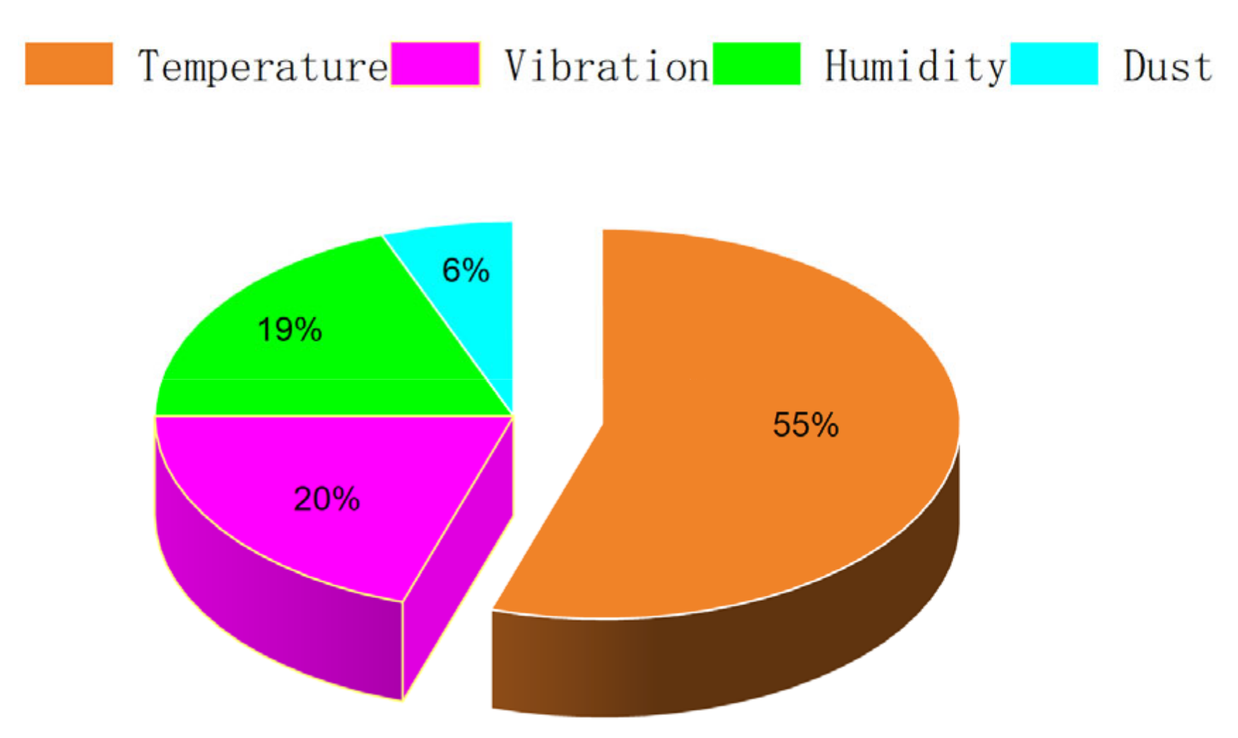
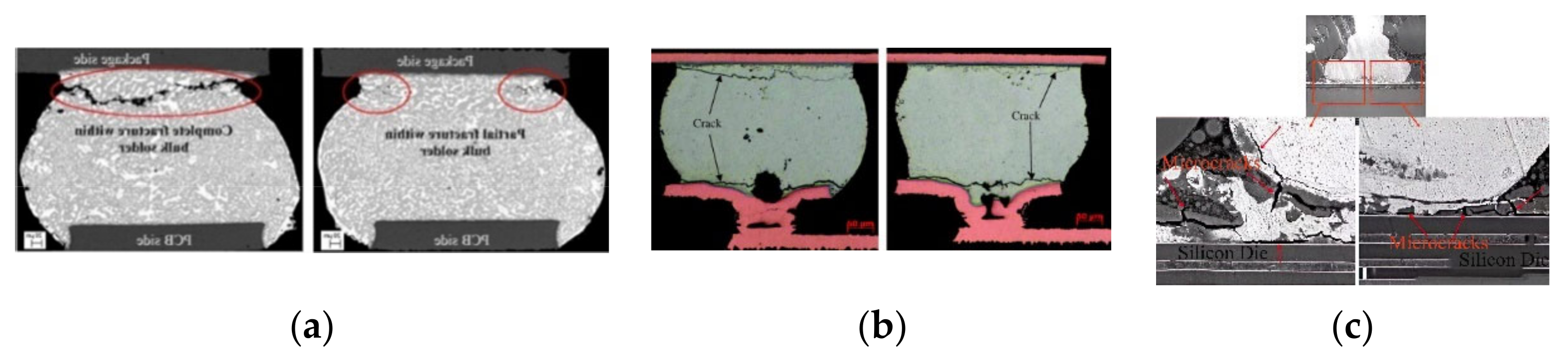
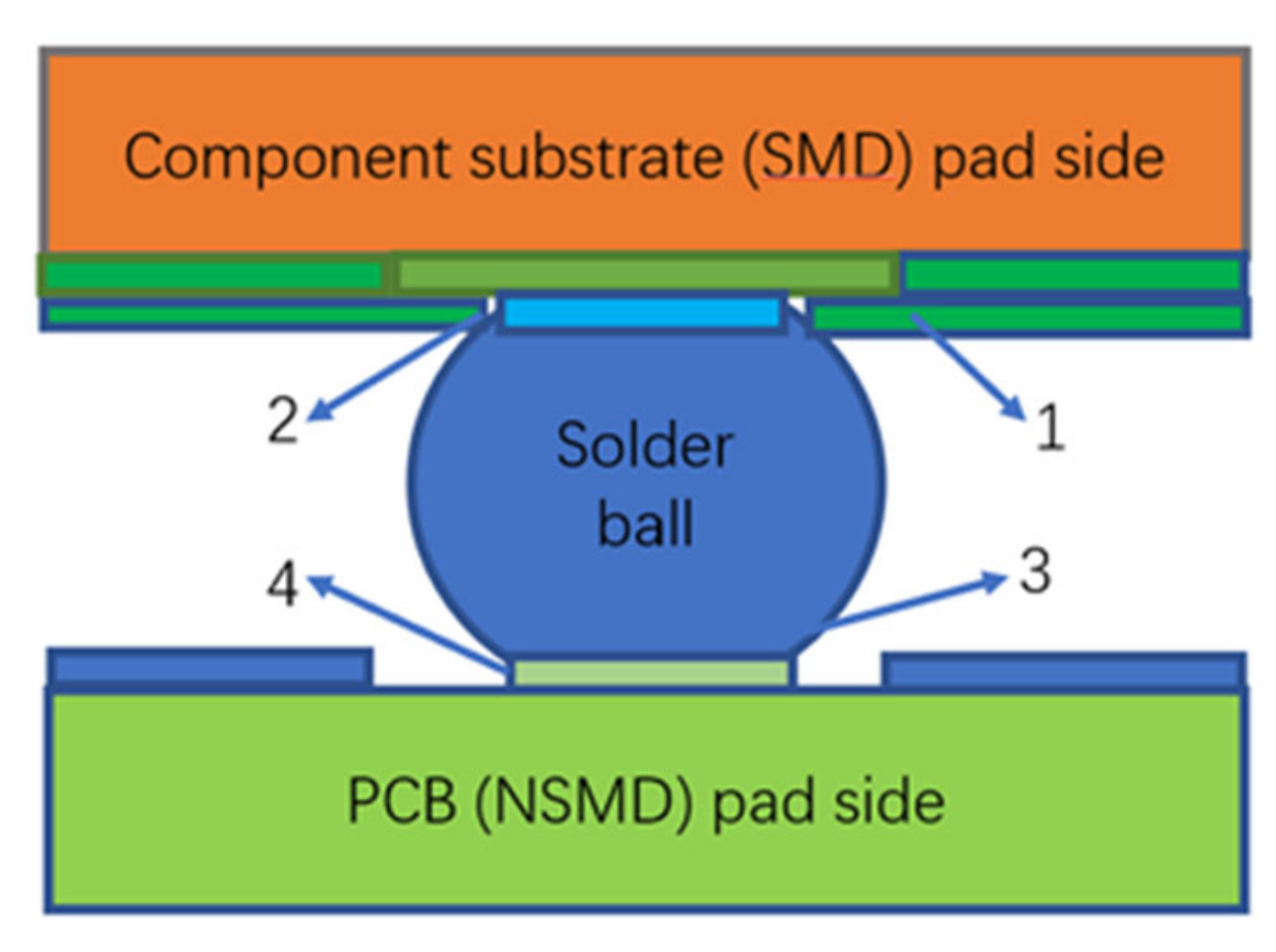
2. Fatigue Failure Factors of BGA Solder Joints
3. Research Methods for Fatigue Failure of BGA Solder Joints
| Test Methods | Test Results | Scopes of Application |
|---|---|---|
| White light interferometer | Geometric size, displacement along the Z direction. Resolution: nanometer. | Used at normal temperature. The sample surface is relatively flat. |
| Electronic speckle interferometer (ESPI) |
Three-direction displacement and deformation. Resolution: 20 nanometers. | Temperature range for the experimental environment: −40~150, component level (including solder joints). |
| Moire interferometer | In-plane displacement and deformation. Resolution: sub-pixel. | Experimental test environment is the same as that for the ESPI. The iso-displacement line can be directly compared with the results obtained by the finite element simulation method. |
| Digital image correlation (DIC) |
In-plane displacement and deformation. Resolution: sub-pixel. | Experimental test environment is the same as that for the ESPI. Large observation range (>cm to 1/10 pixel). It can be combined with a microscope and an SEM. |
| Silicon chip testing | Stress and strain of the chip with the displacement. Resolution: MPa. | Device-level test. Connected in the circuit. It can be applied to the field environment. |
| X-ray reflection | Bending radius of crystal material (such as silicon material). | Experimental environment temperature: −40~120. In principle, internal packaging and testing can be carried out. |
| X-ray diffraction | Mechanical stress and strain of crystalline materials (such as silicon materials). | Experimental environment temperature: −40~120. In principle, internal packaging and testing can be carried out. |
| Scanning electron microscope (SEM) |
In-plane displacement. Resolution: nanometer. | While observing the morphology, the composition of the micro-area is analyzed. |
Another method is to use finite element simulation software to predict the fatigue life of solder joints [49][50]. Finite element software is employed to model and simulate the fatigue failure for specific components or solder joints under specific environmental parameters. Thus, significant information can be achieved, involving the stress and strain of key solder joints. Combined with the real working conditions of the packaging device, a suitable prediction model is selected to predict the fatigue life of the solder joint [46].
3.1. Research Methods for Fatigue Failure of BGA Solder Joints under Vibration Load
3.2. Research Method for Fatigue Failure of Solder Joints under Thermal Stress
3.3. Research Method for Fatigue Failure of Solder Joints under Shear Stress
4. Several Common Models for Fatigue Life Prediction of Solder Joints
4.1. Coffin–Manson Life Model
4.2. Darveaux Life Model
4.3. Paris Life Model
4.4. Creep Life Model
5. Conclusions
This entry is adapted from the peer-reviewed paper 10.3390/electronics11040542
References
- Chung, S.; Kwak, J.B.J.E. Comparative study on reliability and advanced numerical analysis of BGA subjected to product-level drop impact test for portable electronics. Electronics 2020, 9, 1515.
- Ren, J.; Huang, M.L. Board-level drop reliability and fracture behavior of low-temperature soldering Sn–Ag–Cu/Sn–Bi–X hybrid BGA solder joints for consumer electronics. J. Mater. Sci. Mater. Electron. 2021, 32, 15453–15465.
- Lin, Y.; Kang, C.; Chua, L.; Choi, W.K.; Yoon, S.W. Advanced 3D eWLB-PoP (embedded wafer level ball grid array-package on package) technology. In Proceedings of the 2016 IEEE 66th Electronic Components and Technology Conference (ECTC), Las Vegas, NV, USA, 31 May–3 June 2016; pp. 1772–1777.
- Huang, J.; Zhou, M.; Zhang, X.P. The melting characteristics and interfacial reactions of Sn-ball/Sn-3.0 Ag-0.5 Cu-paste/Cu joints during reflow soldering. J. Electron. Mater. 2017, 46, 1504–1515.
- Ye, H.; Xue, S.; Zhang, L.; Ji, F.; Dai, W. Reliability evaluation of CSP soldered joints based on FEM and Taguchi method. Comput. Mater. Sci. 2010, 48, 509–512.
- Jin, Y.; Baraton, X.; Yoon, S.; Lin, Y.; Marimuthu, P.C.; Ganesh, V.; Meyer, T.; Bahr, A. Next generation eWLB (embedded wafer level BGA) packaging. In Proceedings of the 2010 12th Electronics Packaging Technology Conference, Singapore, 8–10 December 2010; pp. 520–526.
- Huang, J.; Zhou, M.; Liang, S.; Zhang, X. Size effects on the interfacial reaction and microstructural evolution of Sn-ball/Sn3.0Ag0.5Cu-paste/Cu joints in board-level hybrid BGA interconnection at critical reflowing temperature. J. Mater. Sci. Mater. Electron. 2018, 29, 7651–7660.
- Gagnon, P.; Fortin, C.; Weiss, T. Package-on-Package Micro-BGA Microstructure Interaction with Bond and Assembly Parameter. In Proceedings of the 2019 IEEE 69th Electronic Components and Technology Conference (ECTC), Las Vegas, NV, USA, 28–31 May 2019; pp. 306–313.
- Petrosyants, K.O.; Ryabov, N.I. Quasi-3D Thermal Model of Stacked IC-TSV-BGA Package. In Proceedings of the 2019 25th International Workshop on Thermal Investigations of ICs and Systems (THERMINIC), Lecco, Italy, 25–27 September 2019; pp. 1–4.
- Kamoji, R.; Oberai, A. Fault Isolation of 2.5 D and 3D Packages through Analysis Across Entire System. In Proceedings of the 2018 IEEE International Symposium on the Physical and Failure Analysis of Integrated Circuits (IPFA), Singapore, 16–19 July 2018; pp. 1–5.
- Shohji, I.; Mori, H.; Orii, Y. Solder joint reliability evaluation of chip scale package using a modified Coffin–Manson equation. Microelectron. Reliab. 2004, 44, 269–274.
- Du, J.H.; Raz, Z.E. A Reliability Qualification Process for BGA Rework Limit. In Proceedings of the 2019 5th International Conference on Control, Automation and Robotics (ICCAR), Beijing, China, 19–22 April 2019; pp. 776–781.
- Tee, T.Y.; Ng, H.S.; Lim, C.T.; Pek, E.; Zhong, Z. Impact life prediction modeling of TFBGA packages under board level drop test. Microelectron. Reliab. 2004, 44, 1131–1142.
- Li, B.; Zhang, X.; Yang, Y.; Yin, L.; Pecht, M. Size and constraint effects on interfacial fracture behavior of microscale solder interconnects. Microelectron. Reliab. 2013, 53, 154–163.
- Loukia, M.; Deshpande, A.; Dasgupta, A. Vulnerability of Copper Pad in BGA Solder Interconnects Under Temperature Cycling. In Proceedings of the 2021 20th IEEE Intersociety Conference on Thermal and Thermomechanical Phenomena in Electronic Systems (iTherm), Marina, San Diego, CA, USA, 31 May–3 June 2021; pp. 679–683.
- Ho, C.; Yang, S.; Kao, C.R. Interfacial reaction issues for lead-free electronic solders. Lead-Free Electron. Solder. 2006, 18, 155–174.
- Park, Y.-S.; Kwon, Y.-M.; Moon, J.-T.; Lee, Y.-W.; Lee, J.-H.; Paik, K.-W. Effects of fine size lead-free solder ball on the interfacial reactions and joint reliability. In Proceedings of the 60th Electronic Components and Technology Conference (ECTC), Las Vegas, NV, USA, 1–4 June 2010; pp. 1436–1441.
- Huang, M.; Yang, F. Size effect on interfacial reactions of Sn–3.0 Ag–0.5 Cu solder balls on Cu and Ni–P pads. J. Mater. Sci. Mater. Electron. 2015, 26, 933–942.
- Gan, G.; Yang, D.; Wu, Y.-p.; Liu, X.; Sun, P.; Xia, D.; Cao, H.; Jiang, L.; Tian, M.J.S.; Technology, S.M. Property of Sn-37Pb solder bumps with different diameter during thermal shock. Solder. Surf. Mt. Technol. 2021, 33, 94–104.
- Ogunsemi, B.T.; Ikubanni, P.P.; Adediran, A.A.; Agboola, O.O. Effect of stand-off height on the shear strength of ball grid array solder joints under varying pad sizes. SN Appl. Sci. 2018, 1, 36.
- Depiver, J.A.; Mallik, S.; Amalu, E.H. Thermal fatigue life of ball grid array (BGA) solder joints made from different alloy compositions. Eng. Fail. Anal. 2021, 125, 105447.
- Liu, F.; Meng, G. Random vibration reliability of BGA lead-free solder joint. Microelectron. Reliab. 2014, 54, 226–232.
- Men, W.; Chen, Y.; Kang, R. Thermal fatigue lifetime prediction of BGA solder joint via a novel fatigue crack propagation model. In Safety and Reliability–Safe Societies in a Changing World; CRC Press: Boca Raton, FL, USA, 2018; pp. 2269–2275.
- Tu, K.-N.; Gusak, A.; Li, M. Physics and materials challenges for lead-free solders. J. Appl. Phys. 2003, 93, 1335–1353.
- Dalton, E.; Ren, G.; Punch, J.; Collins, M.N.J.M. Accelerated temperature cycling induced strain and failure behaviour for BGA assemblies of third generation high Ag content Pb-free solder alloys. Mater. Des. 2018, 154, 184–191.
- Shen, L.; Chen, C.; Niu, X. Random vibration analysis of BGA with different size of the SAC0307 solder joint. In Proceedings of the 2018 19th International Conference on Electronic Packaging Technology (ICEPT), Shanghai, China, 8–11 August 2018; pp. 1019–1021.
- Thanu, D.P.; Antoniswamy, A.; Danaei, R.; Keswani, M. Adhesion Phenomena Pertaining to Thermal Interface Materials and Solder Interconnects in Microelectronic Packaging: A Critical Review. Rev. Adhes. Adhes. 2018, 6, 1–25.
- Tee, T.Y.; Luan, J.-e.; Pek, E.; Lim, C.T.; Zhong, Z. Advanced experimental and simulation techniques for analysis of dynamic responses during drop impact. In Proceedings of the 54th Electronic Components and Technology Conference (IEEE Cat. No. 04CH37546), Las Vegas, NV, USA, 4 June 2004; pp. 1088–1094.
- Yang, Z. An energy-based crack growth criterion for modelling elastic–plastic ductile fracture. Mech. Res. Commun. 2005, 32, 514–524.
- Suhir, E.; Ghaffarian, R.; Nicolics, J. Could thermal stresses in a BGA/CGA-system be evaluated from a model intended for a homogeneously bonded assembly? J. Mater. Sci. Mater. Electron. 2016, 27, 570–579.
- Hwang, J.; Vargas, R.J.S.; Technology, S.M. Solder Joint Reliability—Can Solder Creep? Solder. Surf. Mount Technol. 1990, 2, 38–45.
- Lau, J.H.; Pao, Y.-H. Solder Joint Reliability of BGA, CSP, Flip Chip, and Fine Pitch SMT Assemblies; McGraw-Hill Professional Publishing: New York, NY, USA, 1997.
- Lau, J.H.; Wong, C.; Lee, N.-C.; Lee, S.-W.R. Electronics Manufacturing: With Lead-Free, Halogen-Free, and Conductive-Adhesive Materials; McGraw-Hill Education: New York, NY, USA, 2003.
- Wang, J.; Niu, Y.; Park, S.; Yatskov, A. Modeling and design of 2.5 D package with mitigated warpage and enhanced thermo-mechanical reliability. In Proceedings of the 2018 IEEE 68th Electronic Components and Technology Conference (ECTC), San Diego, CA, USA, 29 May–1 June 2018; pp. 2477–2483.
- Shao, S.; Niu, Y.; Wang, J.; Liu, R.; Park, S.; Lee, H.; Refai-Ahmed, G.; Yip, L. Comprehensive study on 2.5 D package design for board-level reliability in thermal cycling and power cycling. In Proceedings of the 2018 IEEE 68th Electronic Components and Technology Conference (ECTC), San Diego, CA, USA, 29 May–1 June 2018; pp. 1668–1675.
- Depiver, J.A.; Mallik, S.; Amalu, E.H. Comparing and Benchmarking Fatigue Behaviours of Various SAC Solders under Thermo-Mechanical Loading. In Proceedings of the 2020 IEEE 8th Electronics System-Integration Technology Conference (ESTC), Tønsberg, Norway, 15–18 September 2020; pp. 1–11.
- Hamasha, S.; Qasaimeh, A.; Jaradat, Y.; Borgesen, P. Correlation between solder joint fatigue life and accumulated work in isothermal cycling. IEEE Trans. Compon. Packag. Manuf. Technol. 2015, 5, 1292–1299.
- Qasaimeh, A.; Hamasha, S.d.; Jaradat, Y.; Borgesen, P. Damage evolution in lead free solder joints in isothermal fatigue. J. Electron. Packag. Trans. ASME 2015, 137, 021012.
- Obaidat, M.; Hamasha, S.; Jaradat, Y.; Qasaimeh, A.; Arfaei, B.; Anselm, M.; Borgesen, P. Effects of varying amplitudes on the fatigue life of lead free solder joints. In Proceedings of the 2013 IEEE 63rd Electronic Components and Technology Conference, Las Vegas, NV, USA, 28–31 May 2013; pp. 1308–1314.
- Batieha, F.; Hamasha, S.; Jaradat, Y.; Wentlent, L.; Qasaimeh, A.; Borgesen, P. Challenges for the prediction of solder joint life in long term vibration. In Proceedings of the 2015 IEEE 65th Electronic Components and Technology Conference (ECTC), San Diego, CA, USA, 26–29 May 2015; pp. 1553–1559.
- Borgesen, P.; Wentlent, L.; Khasawneh, S.; Shirazi, S.; Schmitz, D.; Alghoul, T.; Greene, C.; Yin, L. A mechanistic thermal fatigue model for SnAgCu solder joints. J. Electron. Mater. 2018, 47, 2526–2544.
- Hamasha, S.d.; Borgesen, P. Effects of strain rate and amplitude variations on solder joint fatigue life in isothermal cycling. J. Electron. Packag. 2016, 138, 021002.
- Su, S.; Akkara, F.; Dawahdeh, A.; Borgesen, P.; Qasaimeh, A. Solder joint reliability in isothermal varying load cycling. In Proceedings of the 2017 16th IEEE Intersociety Conference on Thermal and Thermomechanical Phenomena in Electronic Systems (ITherm), Orlando, FL, USA, 30 May–2 June 2017; pp. 1331–1336.
- Su, S.; Jian, M.; Akkara, F.J.; Hamasha, S.d.; Suhling, J.; Lall, P. Fatigue and shear properties of high reliable solder joints for harsh applications. In Proceedings of the SMTA International, Rosemont, IL, USA, 14–18 October 2018.
- Hamasha, S.; Akkara, F.; Su, S.; Ali, H.; Borgesen, P. Effect of cycling amplitude variations on SnAgCu solder joint fatigue life. IEEE Trans. Compon. Packag. Manuf. Technol. 2018, 8, 1896–1904.
- Qi, H.; Osterman, M.; Pecht, M. A rapid life-prediction approach for PBGA solder joints under combined thermal cycling and vibration loading conditions. IEEE Trans. Compon. Packag. Manuf. Technol. 2009, 32, 283–292.
- Pustan, D.; Wilde, J. Modern test methods for a comprehensive thermo-mechanical deformation analysis in area-array-assemblies. In Proceedings of the 2008 58th Electronic Components and Technology Conference, Lake Buena Vista, FL, USA, 27–30 May 2008; pp. 599–605.
- Syed, A. Overview of Reliability Models and Data Needs. In Proceedings of the Workshop on modeling and Data Needs for Lead-Free Solders, New Orleans, LA, USA, 15 February 2001.
- Muhammad Nubli, Z. Temperature Cycling Test for a Ball Grid Array (BGA) Package Using Finite Element Analysis (FEA). Master’s Thesis, University Malaysia Perlis, Perlis, Malaysia, January 2008.
- Ying, C.; Zebing, H.; Rui, K. Lifetime prediction and impact factors analysis of ball grid array solder joint based on FEA. In Proceedings of the 2010 11th International Conference on Electronic Packaging Technology & High Density Packaging, Xi’an, China, 16–19 August 2010; pp. 1142–1146.
- Steinberg, D.S. Vibration Analysis for Electronic Equipment; Wiley: Hoboken, NJ, USA, 2000.
- Kinyanjui, R.; Chu, Q.; Snugovsky, P.; Coyle, R. Solder Joint Reliability of Pb-free SnAgCu Ball Grid Array (BGA) Components in SnPb Assembly Process. Proc. APEX 2008, 2008, S02–S15.
- Liu, F.; Lu, Y.; Wang, Z.; Zhang, Z. Numerical simulation and fatigue life estimation of BGA packages under random vibration loading. Microelectron. Reliab. 2015, 55, 2777–2785.
- Shen, Y.-L. Thermo-mechanical stresses in copper interconnects—A modeling analysis. Microelectron. Eng. 2006, 83, 446–459.
- Lau, J. Thermal Stress and Strain in Microelectronics Packaging; Springer Science & Business Media: Berlin/Heidelberg, Germany, 2012.
- Noda, N.; Hetnarski, R.B.; Tanigawa, Y. Thermal Stresses; Routledge: London, UK, 2018.
- Vasudevan, V.; Coyle, R.; Aspandiar, R.; Tisdale, S.; Kinyanjui, R.; Long, G. Thermal cycling reliability, microstructural characterization, and assembly challenges with backward compatible soldering of a large, high density ball grid array. In Proceedings of the 2011 IEEE 61st Electronic Components and Technology Conference (ECTC), Lake Buena Vista, FL, USA, 31 May–3 June 2011; pp. 954–964.
- Koo, J.-M.; Jung, S.-B. Effect of displacement rate on ball shear properties for Sn–37Pb and Sn–3.5 Ag BGA solder joints during isothermal aging. Microelectron. Reliab. 2007, 47, 2169–2178.
- Chapetti, M.D.; Jaureguizahar, L. Fatigue behavior prediction of welded joints by using an integrated fracture mechanics approach. Int. J. Fatigue 2012, 43, 43–53.
- Yang, Q.; Shim, D.; Spearing, S. A cohesive zone model for low cycle fatigue life prediction of solder joints. Microelectron. Eng. 2004, 75, 85–95.
- Knecht, S.; Fox, L. Integrated matrix creep: Application to accelerated testing and lifetime prediction. In Solder Joint Reliability; Springer: Berlin/Heidelberg, Germany, 1991; pp. 508–544.
- Solomon, H. Fatigue of 60/40 solder. IEEE Trans. Compon. Hybrid Manuf. Technol. 1986, 9, 423–432.
- Sornette, D.; Magnin, T.; Brechet, Y.J.E. The physical origin of the Coffin-Manson law in low-cycle fatigue. Europhys. Lett. 1992, 20, 433.
- Feltner, C.E.; Morrow, J.D. Microplastic strain hysteresis energy as a criterion for fatigue fracture. J. Basic Eng. 1961, 83, 15–22.
- Bhate, D.; Subbarayan, G. A nonlinear fracture mechanics prespective on solder joint failure: Going beyond the coffin-manson equation. In Proceedings of the Thermal and Thermomechanical Proceedings 10th Intersociety Conference on Phenomena in Electronics Systems, San Diego, CA, USA, 30 May–2 June 2006; pp. 1220–1225.
- Qu, X.; Chen, Z.; Qi, B.; Lee, T.; Wang, J.J. Board level drop test and simulation of leaded and lead-free BGA-PCB assembly. Microelectron. Reliab. 2007, 47, 2197–2204.
- Xiao, H.; Li, X.; Hu, Y.; Guo, F.; Shi, Y. Damage behavior of SnAgCu/Cu solder joints subjected to thermomechanical cycling. J. Alloys Compd. 2013, 578, 110–117.
- Paris, P.; Erdogan, F. A critical analysis of crack propagation laws. J. Basic Eng. 1963, 85, 528–533.
- Pugno, N.; Ciavarella, M.; Cornetti, P.; Carpinteri, A. A generalized Paris’ law for fatigue crack growth. J. Mech. Phys. Solids 2006, 54, 1333–1349.
- Lee, W.; Nguyen, L.; Selvaduray, G. Solder joint fatigue models: Review and applicability to chip scale packages. Microelectron. Reliab. 2000, 40, 231–244.
- Depiver, J.a.; Mallik, S.; Harmanto, D. Solder joint failures under thermo-mechanical loading conditions—A review. Adv. Mater. Process. Technol. 2021, 7, 1–26.
- Shrestha, T.; Gollapudi, S.; Charit, I.; Murty, K.L. Creep deformation behavior of Sn–Zn solder alloys. J. Mater. Sci. 2014, 49, 2127–2135.