Your browser does not fully support modern features. Please upgrade for a smoother experience.
Please note this is an old version of this entry, which may differ significantly from the current revision.
Subjects:
Computer Science, Artificial Intelligence
|
Nanoscience & Nanotechnology
|
Engineering, Electrical & Electronic
Layered two-dimensional (2D) and quasi-zero-dimensional (0D) materials effectively absorb radiation in the wide ultraviolet, visible, infrared, and terahertz ranges. Photomemristive structures made of such low-dimensional materials are of great interest for creating optoelectronic platforms for energy-efficient storage and processing of data and optical signals in real time.
- photomemristors
- graphene
- machine vision
1. Introduction
In recent years, there has been an increased interest in the creation of optoelectronic devices based on photomemristors capable of energy-saving storage and processing of signals, such as neurons and synapses in biological systems [1]. The need to improve the speed and energy efficiency of big data processing is especially acute in systems such as artificial intelligence (AI) in autopilot and autonomous unmanned vehicles. In 2021, Elon Musk presented the development of the D1 Dojo processor for the AI of the Tesla autopilot, designed to work in neural networks for pattern recognition [2]. The D1 Dojo is manufactured using 7 nm complementary metal-oxide semiconductor (CMOS) technology, has an area of 645 mm2, and contains 50 billion transistors (5 × 10¹⁰/mm2 ~ 4 × 109 cm2). For comparison, the density of conventionally computational and memory elements in the human brain is −1011 (neurons) and 1015 (synapses), respectively. A computer with a variable set D1 (Figure 1), built on the basis of 3000 such chips, would perform 1018 operations per second (1.1 EFLOPS) and consume 1.2 MW (a board of 25 chips with heat removal up to 15 kW consumes ~10 kW) [2].
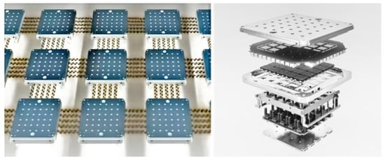
Figure 1. A set of D1 Dojo processors (2021) for Tesla’s AI autopilot, designed to work in neural networks (left). The design of the processor, consisting of various plates: heat sink, computation, and power and control (right).
The so-called “in-memory computing” can improve the energy efficiency of computations using memristor circuits similar to biological neural networks [4,5,6,7,8,9]. Significant research progress has been made in improving the performance of memristive devices based on 2D layered materials [10,11,12]. Two-dimensional layered materials have unique physical properties and open up great opportunities for applications in neuromorphic computing. However, to solve the problem of time delay in processing the detected signal, new approaches are needed to create photoelectronic components of AI visual systems. One such approach is “photodetecting and computing in-memory”. The development of AI systems for automatic control (piloting) of machines in an autonomous mode requires the development of a fundamentally new element base of sensor and computing devices that allow detecting and processing information in real time. Memristor structures made of photosensitive low-dimensional layered materials [13,14,15,16], which effectively absorb radiation in the ultraviolet, visible, and infrared ranges [17,18,19], can be used as an optoelectronic platform embedded in CMOS technology for fast and energy-efficient neuromorphic processing of an optical signal and pattern recognition.
2. Photomemristor
A photomemristor made from MoS2 crystals was demonstrated in 2016 [15]. Polarization of the memristor in an electric field upon excitation by light led to multilevel switching. The faster polarization process of the photomemristor in comparison with the transport of ions and the fast optical access make it possible to detect and quickly process signals in the memory.
Figure 3 shows the switching diagrams of the MoS2 photomemristor by electrical and optical pulses. The memristor, polarized at different voltages, shows eight different states that can be read electrically under optical excitation. The photomemristor provides fast multi-level non-linear dynamic operation and can be used for image detection and processing.
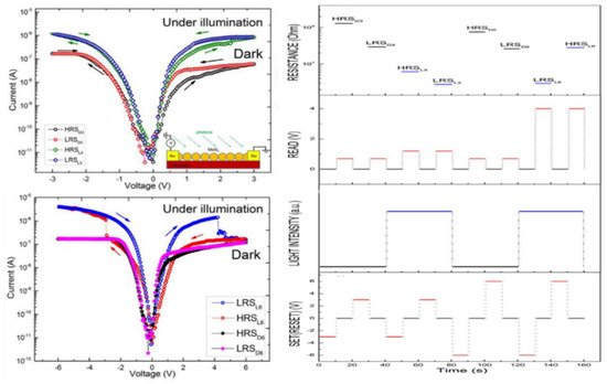
Figure 3. Current–voltage characteristics of the MoS2 photomemristor polarized at 3V (left, top) and 6V (left, bottom) and switching diagrams (SET, RESET) of memristive states (HRSD3, HRSL3, LRSD3, LRSL3, HRSD6, HRSL6, LRSD6, LRSL6) with electrical and optical excitation [15].
A photomemristor has also been demonstrated based on two-dimensional materials graphene (G) and graphene oxide (GO) [20]. It has been shown that the photocatalytic oxidation of graphene with ZnO nanoparticles creates self-assembling photosensitive G/GO heterostructures exhibiting photomemristive states.
3. Photosensitive 2D Crystals and Their Embedding in CMOS Technology
Two-dimensional crystals have great potential to operate in a wide spectral range from UV to THz [21,22,23,24,25,26]. Most of them cover the visible and short-wave infrared range (Figure 5).
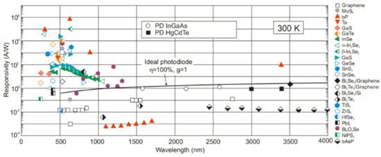
Figure 5. Spectral sensitivity of photodetectors made of 2D layered materials at 300 K. The black line shows the spectral sensitivity of an ideal photodiode with 100% QE and g = 1. The sensitivity of commercially available photodetectors (InGaAs and HgCdTe photodiodes) is presented for comparison [21].
The uniqueness of the atomic surface of 2D materials without dangling bonds allows crystals to be embedded in CMOS technology without introducing structural defects, which makes it possible to produce high-quality functional integrated circuits for broadband detection.
CMOS-integrated circuits, which are at the heart of the microelectronics technological revolution, enable the creation of compact and inexpensive microelectronic circuits and imaging systems. However, the use of this platform in applications other than microcircuits and visible light cameras is hampered by the difficulty of combining non-silicon semiconductors with CMOS technology.
4. Photocells Based on 2D Crystals and Nanocomposites
Two-dimensional semiconductors provide unique opportunities for optoelectronics due to their layered atomic structure and optical and electronic properties. To date, most of the applied research in this area is focused on field-effect electronics, as well as photodetectors and LEDs. The photonic and electronic design of a 2D semiconductor photovoltaic system represents a new direction for ultra-thin, efficient solar cells with applications ranging from portable and ultra-lightweight optoelectronic battery power generation to intelligent photosensors. The absorption of light in the active layers of a photovoltaic cell is one of the key performance indicators that determines the efficiency of a device. For semiconductors, including 2D materials, absorption is determined by the structure of the electron band and the band gap.
5. Layered Quantum Dots
Layered materials have recently emerged as layered atomically thin QDs consisting of only a few layers or even a single layer of material with transverse dimensions of less than 10 nm [28,29,30,31,32,33,34,35]. The band gap of such QDs can be tuned by optimizing their lateral size and the number of layers. Layered QDs have unique luminescent, adsorption, and chemical properties due to their inherent two-dimensional structure. Most layered QDs retain their two-dimensional lattices from their bulk form, but with improved solution dispersibility and surface functionalization capabilities. With a greater surface area, higher solubility, and heterostructure formation flexibility, QD-based devices can be modified to provide better performance and stability characteristics [34,35].
The formation of quantum dots consisting of one or several 4H-SnS2 layers was demonstrated by the liquid-phase separation method [28]. With a decrease in their size, a systematic shift of the peaks in the Raman and absorption spectra was observed.
6. Ultrafast and Highly Sensitive IR Photosensors Based on 2D Crystals for Pattern Recognition
Detection and sensing by infrared light are widely used in modern technologies, which are based on various photovoltaic materials. The emergence of 2D materials, due to their excellent electronic structure, extreme size limitation, and strong interaction of light and matter, creates a unique platform for the development of next-generation infrared photosensors [38,39,40,41].
Many 2D materials exhibit high environmental and chemical resistance, ideal mechanical, electronic, and optical properties required for industrial applications [48,49,50,51,52,53]. Ideal infrared detectors have fast response times, high sensitivity, and environmental resistance, which are rarely found simultaneously in the same two-dimensional material.
7. Conclusions
Low-dimensional layered (LDL) photosensitive memristive materials and structures offer good scalability, and the potential for photodetection and in-memory computing is seen as a promising candidate for next-generation broadband CMOS-compatible image-recognition devices for AI applications in autonomous unmanned vehicles. Photomemristor and photosensor structures based on two-dimensional crystals and van der Waals heterostructures are a new class of optoelectronic components for autonomous energy-saving neuromorphic visual information processing systems. The use of a floating QD photogate makes it possible to optically control multilevel photomemristive states in a wide visible–IR range.
Another important issue of LDL materials for photosynaptic applications is reliability. The quality of LDL material crystals, a key factor in desired photosynaptic operations, depends on various synthesis conditions or growth methods. In addition, at present, many studies are mainly focused on the optical and electrical properties of LDL materials, while more attention to their mechanical and magnetic properties can significantly improve the performance of photomemristive sensors. Photodetectors based on LDL materials are of great interest due to their wide photodetection range, high sensitivity, flexibility, and potentially small size. With these advantages, it is possible to revolutionize the mid-IR photodetector industry in favor of compact, small-sized and low-cost visible–IR smart photodetectors that can be used in an AI visual system. The nature of the atomic layer and the broadband photoresponse of LDL materials will be an important part of the next-generation broadband artificial vision industry. However, it remains a big challenge to obtain LDL photosensors with high response speed, high gain, and high detectability at the same time, especially in the mid- and far-IR range. Bismuth oxyselenide has excellent physical properties due to its unique crystal configuration and electronic structure, such as ultra-high mobility, good mechanical flexibility, and broadband optical response. Due to its oxygen-containing composition, its remarkable stability makes it a competitive candidate for practical applications in optoelectronics. However, a simple, large-scale, and inexpensive synthesis of the LDL bismuth oxyselenide structure remains a challenging task. Most existing LDL photomemristive devices currently cannot meet the requirements of a commercially ideal photoelectronic synapses.
This entry is adapted from the peer-reviewed paper 10.3390/electronics11040619
This entry is offline, you can click here to edit this entry!