Interpenetrating bulk heterojunction (IBHJ) quantum dot solar cells (QDSCs) offer a direct pathway for electrical contacts to overcome the trade-off between light absorption and carrier extraction. However, their complex three-dimensional structure creates higher requirements for the optimization of their design due to their more difficult interface defect states control, more complex light capture mechanism, and more advanced QD deposition technology. ZnO nanowire (NW) has been widely used as the electron transport layer (ETL) for this structure. Hence, the optimization of the ZnO NW morphology (such as density, length, and surface defects) is the key to improving the photoelectric performance of these SCs.
- interpenetrating bulk heterojunction
- quantum dot solar cells
- ZnO nanowire
- synthetic method
- geometric optimization
- defect passivation
1. Introduction
2. Optimization Strategies of IBHJ QDSCs Based on ZnO NWs
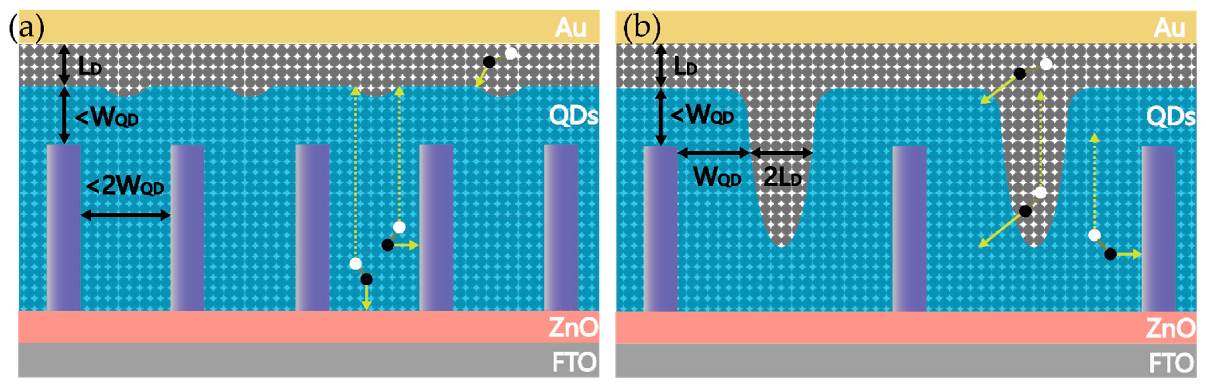
2.1. Geometrical Morphology Optimization of Nanowires


| Ligand | CQD Material | CQDSC Structure | Doping Density (cm−3) | Depletion Width (nm) | Diffusion Lengths (nm) | PCE (%) |
|---|---|---|---|---|---|---|
| Organic ligand | PbS-MPA [39] |
- | - | - | 30 | - |
| PbS-MPA [40] |
- | - | - | 70 | - | |
| Halide ligand | PbS-PbX2 [41] |
ITO/ZnO/PbS-PbX2/PbS-EDT/Au | 9.94 × 10¹⁶ | 165 | 52 | 7.2 |
| PbO-PbS-TBAI [42] |
ITO/ZnO/PbS-TBAI/PbS-EDT/Au | - | - | 61 | 9.4 | |
| PbAc-PbS-TBAI [42] |
ITO/ZnO/PbS-TBAI/PbS-EDT/Au | - | - | 95 | 10.8 | |
| PbS-TBAI [39] |
- | - | - | 70 | - | |
| PbS-TBAI [43] |
ITO/ZnO/PbS-TBAI/PbS-EDT/Au | 7.3 × 10¹⁶ | 61.0 (at maximum PCE) |
85 | 8.7 | |
| PbS-I2 + TBAI [43] |
ITO/ZnO/PbS-I2 + TBAI/PbS-EDT/Au | 6.8 × 10¹⁶ | 62.5 (at maximum PCE) |
115 | 10.1 | |
| Hybrid ligand | PbS-MPA + CdCl2 [44] |
FTO/ZnO/PbS-MPA +CdCl2/MoOx/Au/Ag | 1 × 10¹⁵–1 × 10¹⁶ | - | 80 | 7.6 |
| PbS-PbX2 + MPE [41] |
ITO/ZnO/PbS-PbX2 + MPE/PbS-EDT/Au | 1.96 × 10¹⁶ | 288 | 94 | 9.6 | |
| PbS-MPA/CdCl2 [40] |
- | - | - | 230 | - |
2.2. Passivation of Defects in Nanowires
| Passivation Strategy | CQDSC Structure | - | Jsc (mA/cm2) | Voc (mV) | FF | PCE (%) |
|---|---|---|---|---|---|---|
| H-plasma-passivation [56] | ITO/ZnO NWs/PbS-TBAI/PbS-EDT/Au | non-treated | 30.0 | 591 | 0.56 | 9.9 |
| H-plasma treated | 31.1 | 610 | 0.57 | 10.8 | ||
| ABA-passivation [35] | ITO/ZnO NWs/PbS-TBAI/PbS-EDT/Au | non-treated | 27.4 | 510 | 0.60 | 8.41 |
| ABA-treated | 27.5 | 540 | 0.64 | 9.52 | ||
| Mg(OH)2 [58] | FTO/ZnO NWs/PbS-TBAI/PbS-EDT/Au | without Mg(OH)2 | 22.62 | 390 | 45.66 | 4.03 |
| with Mg(OH)2 | 21.51 | 520 | 45.08 | 5.04 | ||
| SnO2 [59] | FTO/ZnO NWs/PbS-CTAB/Au | without SnO2 | 20.4 | 580 | 0.47 | 5.55 |
| with SnO2 | 23.2 | 603 | 0.56 | 7.78 | ||
| CBD-TiO2 [55] | FTO/ZnO NWs/PbS-CTAB/Au | without TiO2 | 28.7 | 279 | 0.430 | 3.50 |
| with TiO2 | 30.7 | 420 | 0.478 | 6.16 | ||
| ALD-TiO2 [57] | FTO/ZnO NWs/PbS-TBAI/PbS-EDT/Au | without TiO2 | 25.3 | 505 | 0.54 | 6.9 |
| with TiO2 | 26.0 | 497 | 0.56 | 7.2 |
2.3. Other Optimization Strategies
3. Conclusions
- (1) The HT method is more suitable for the large-scale application of IBHJ QDSCs due to its advantages of low temperature, high yield, and easy processing. The morphology of HT-grown NWs is influenced by the seed layer properties, growth time, concentration, temperatures, PH, and post-treatment conditions. However, it is necessary to investigate the mechanism of these influencing factors for the preparation of NWs with controllable morphologies. Furthermore, the optimization of surface defects and internal defects and the reliability of HT-doping elements also need to be studied further to improve the performance of the ETL and to tune the band-gap arrangement.
- (2) The density of the NW affects the filling volume of QD materials. High-density NW arrays not only feature a large VOC loss due to their large interface area, but also cause high reflectivity in the SCs, reducing the light absorption. The length of the nanowires determines the depth of the carrier collection and further affects the thickness of the SCs. However, long NWs often result in poor hole collection and increase the interface area. In addition, the length of the nanowires affects the light trapping effect of the 3D structure, and may cause the aggregation of light absorption and ultimately affect the recombination of the carriers.
- (3) The geometric morphology of the NW exerts a great influence on the transmission and collection of photocarriers. The optimization of NW spacing needs to take account of the transverse collection of electrons, while the length of the NW and the thickness of the SC absorption layer need to be determined after comprehensively analyzing the longitudinal aggregation of holes. In order to satisfy the carrier collection conditions as far as possible, reducing the NW density can increase the filling volume of QD light absorption material.
- (4) In order to further optimize the 3D structure, more accurate carrier transport mechanism analysis needs to be carried out in combination with electrical simulation to determine the optimal electrical structure. The light-trapping effect caused by NWs also needs to be more accurately analyzed, since poor light scattering may lead to local light aggregation and thus affect the distribution and collection efficiency of photocarriers.
- (5) The passivation of the NW surface is an important way to improve the VOC of IBHJ QDSCs. Passivation strategies commonly include post-annealing, H-plasma treatment, and ABA surface treatment. Moreover, the addition of Mg(OH)2, SnO2, and TiO2 buffer layers on the surface of NWs also effectively improves the performance of SCs. However, the effects of the passivation layer (including the passivation mechanism of the defects and the band arrangement of the battery) on the three-dimensional heterojunction remain to be explored. A comparative study of different passivation layers may be helpful in this regard.
This entry is adapted from the peer-reviewed paper 10.3390/nano12010114
References
- Gil, L.; Bernardo, J. An Approach to Energy and Climate Issues Aiming at Carbon Neutrality. Renew. Energy Focus 2020, 33, 37–42.
- Khalid, S.; Sultan, M.; Ahmed, E.; Ahmed, W. Chapter 1-Third-Generation Solar Cells. In Emerging Nanotechnologies for Renewable Energy; Ahmed, W., Booth, M., Nourafkan, E., Eds.; Micro and Nano Technologies; Elsevier: Amsterdam, The Netherlands, 2021.
- Green, M.; Emery, K.; Hishikawa, Y.; Warta, W.; Dunlop, E.; Barkhouse, D.; Gunawan, O.; Gokmen, T.; Todorov, T.; Mitzi, D. Solar cell efficiency tables (version 40). IEEE Trans. Fuzzy Syst. 2012, 20, 1114–1129.
- Weller, H. Colloidal Semiconductor Q-Particles: Chemistry in the Transition Region Between Solid State and Molecules. Angew. Chemie Int. Ed. English 1993, 32, 41–53.
- Schaller, R.D.; Klimov, V.I. High Efficiency Carrier Multiplication in PbSe Nanocrystals: Implications for Solar Energy Conversion. Phys. Rev. Lett. 2004, 92, 1–4.
- Goodwin, H.; Jellicoe, T.C.; Davis, N.J.L.K.; Böhm, M.L. Multiple Exciton Generation in Quantum Dot-Based Solar Cells. Nanophotonics 2018, 7, 111–126.
- Knig, D.; Casalenuovo, K.; Takeda, Y.; Conibeer, G.; Guillemoles, J.F.; Patterson, R.; Huang, L.M.; Green, M.A. Hot Carrier Solar Cells: Principles, Materials and Design. Phys. E Low-Dimensional Syst. Nanostruct. 2010, 42, 2862–2866.
- Marti, A.; Cuadra, L.; Luque, A. Quantum Dot Intermediate Band Solar Cell. Conf. Rec. IEEE Photovolt. Spec. Conf. 2000, 2000, 940–943.
- Luque, A.; Martí, A. The Intermediate Band Solar Cell: Progress toward the Realization of an Attractive Concept. Adv. Mater. 2010, 22, 160–174.
- Asahi, S.; Kaizu, T.; Kita, T. Adiabatic Two-Step Photoexcitation Effects in Intermediate-Band Solar Cells with Quantum Dot-in-Well Structure. Sci. Rep. 2019, 9, 1–8.
- McMeekin, D.P.; Mahesh, S.; Noel, N.K.; Klug, M.T.; Lim, J.C.; Warby, J.H.; Ball, J.M.; Herz, L.M.; Johnston, M.B.; Snaith, H.J. Solution-Processed All-Perovskite Multi-Junction Solar Cells. Joule 2019, 3, 387–401.
- Ikeri, H.I.; Onyia, A.I.; Vwavware, O.J. The Dependence of Confinement Energy on the Size of Quantum Dots. Int. J. Sci. Res. Phys. Appl. Sci. 2019, 7, 27–30.
- Shockley, W.; Queisser, H.J. Detailed Balance Limit of Efficiency of P-n Junction Solar Cells. J. Appl. Phys. 1961, 32, 510–519.
- Johnston, K.W.; Pattantyus-Abraham, A.G.; Clifford, J.P.; Myrskog, S.H.; MacNeil, D.D.; Levina, L.; Sargent, E.H. Schottky-Quantum Dot Photovoltaics for Efficient Infrared Power Conversion. Appl. Phys. Lett. 2008, 92, 1–4.
- Piliego, C.; Protesescu, L.; Bisri, S.Z.; Kovalenko, M.V.; Loi, M.A. 5.2% Efficient PbS Nanocrystal Schottky Solar Cells. Energy Environ. Sci. 2013, 6, 3054–3059.
- Zhang, Y.; Ding, C.; Wu, G.; Nakazawa, N.; Chang, J.; Ogomi, Y.; Toyoda, T.; Hayase, S.; Katayama, K.; Shen, Q. Air Stable PbSe Colloidal Quantum Dot Heterojunction Solar Cells: Ligand-Dependent Exciton Dissociation, Recombination, Photovoltaic Property, and Stability. J. Phys. Chem. C 2016, 120, 28509–28518.
- Spencer, B.F.; Leontiadou, M.A.; Clark, P.C.J.; Williamson, A.I.; Silly, M.G.; Sirotti, F.; Fairclough, S.M.; Tsang, S.C.E.; Neo, D.C.J.; Assender, H.E.; et al. Charge Dynamics at Heterojunctions for PbS/ZnO Colloidal Quantum Dot Solar Cells Probed with Time-Resolved Surface Photovoltage Spectroscopy. Appl. Phys. Lett. 2016, 108.
- Pattantyus-Abraham, A.G.; Kramer, I.J.; Barkhouse, A.R.; Wang, X.; Konstantatos, G.; Debnath, R.; Levina, L.; Raabe, I.; Nazeeruddin, M.K.; Gratzel, M. Depleted-Heterojunction Colloidal Quantum Dot Solar Cells. ACS Nano 2010, 4, 3374–3380.
- Rath, A.K.; Bernechea, M.; Martinez, L.; Pelayo Garcia De Arquer, F.; Osmond, J.; Konstantatos, G. Solution-Processed Inorganic Bulk Nano-Heterojunctions and Their Application to Solar Cells. Nat. Photonics 2012, 6, 529–534.
- Tang, J.; Liu, H.; Zhitomirsky, D.; Hoogland, S.; Wang, X.; Furukawa, M.; Levina, L.; Sargent, E.H. Quantum Junction Solar Cells. Nano Lett. 2012, 12, 4889–4894.
- Jia, Y.; Wang, H.; Wang, Y.; Shibayama, N.; Kubo, T.; Liu, Y.; Zhang, X.; Segawa, H. High-Performance Electron-Transport-Layer-Free Quantum Junction Solar Cells with Improved Efficiency Exceeding 10%. ACS Energy Lett. 2021, 493–500.
- Chang, C.H.; Lee, Y.L. Chemical Bath Deposition of CdS Quantum Dots onto Mesoscopic TiO2 Films for Application in Quantum-Dot-Sensitized Solar Cells. Appl. Phys. Lett. 2007, 91, 2–5.
- Kamat, P.V.; Bang, J.H. Quantum Dot Sensitized Solar Cells: Tale of Two Semiconductor Nanocrystals—CdSe and CdTe. ACS Natl. Meet. B. Abstr. 2009, 3, 1467–1476.
- Sahu, A.; Garg, A.; Dixit, A. A Review on Quantum Dot Sensitized Solar Cells: Past, Present and Future towards Carrier Multiplication with a Possibility for Higher Efficiency. Sol. Energy 2020, 203, 210–239.
- Choi, M.J.; García de Arquer, F.P.; Proppe, A.H.; Seifitokaldani, A.; Choi, J.; Kim, J.; Baek, S.W.; Liu, M.; Sun, B.; Biondi, M.; et al. Cascade Surface Modification of Colloidal Quantum Dot Inks Enables Efficient Bulk Homojunction Photovoltaics. Nat. Commun. 2020, 11, 1–9.
- Beard, M.C.; Luther, J.M.; Semonin, O.E.; Nozik, A.J. Third Generation Photovoltaics Based on Multiple Exciton Generation in Quantum Confined Semiconductors. Acc. Chem. Res. 2013, 46, 1252–1260.
- Johnston, K.W.; Pattantyus-Abraham, A.G.; Clifford, J.P.; Myrskog, S.H.; Hoogland, S.; Shukla, H.; Klem, E.J.D.; Levina, L.; Sargent, E.H. Efficient Schottky-Quantum-Dot Photovoltaics: The Roles of Depletion, Drift, and Diffusion. Appl. Phys. Lett. 2008, 92, 1–4.
- Fan, Z.; Razavi, H.; Do, J.W.; Moriwaki, A.; Ergen, O.; Chueh, Y.L.; Leu, P.W.; Ho, J.C.; Takahashi, T.; Reichertz, L.A.; et al. Three-Dimensional Nanopillar-Array Photovoltaics on Low-Cost and Flexible Substrates. Nat. Mater. 2009, 8, 648–653.
- Kayes, B.M.; Atwater, H.A.; Lewis, N.S. Comparison of the Device Physics Principles of Planar and Radial P-n Junction Nanorod Solar Cells. J. Appl. Phys. 2005, 97, 114302.
- Garnett, E.; Yang, P. Light Trapping in Silicon Nanowire Solar Cells. Nano Lett. 2010, 10, 1082–1087.
- Krogstrup, P.; Jørgensen, H.I.; Heiss, M.; Demichel, O.; Holm, J.V.; Aagesen, M.; Nygard, J.; Fontcuberta i Morral, A. Single-Nanowire Solar Cells beyond the Shockley-Queisser Limit. Nat. Photonics 2013, 7, 306–310.
- Wang, Y.; Su, W.; Zang, S.; Li, M.; Zhang, X.; Liu, Y. Bending-Durable Colloidal Quantum Dot Solar Cell Using a ZnO Nanowire Array as a Three-Dimensional Electron Transport Layer. Appl. Phys. Lett. 2017, 110, 1–6.
- Tavakoli Dastjerdi, H.; Prochowic, D.; Yadav, P.; Tavakoli, M.M. Luminescence Down-Shifting Enables UV-Stable and Efficient ZnO Nanowire-Based PbS Quantum Dot Solar Cells with JSC Exceeding 33 MA Cm−2. Sustain. Energy Fuels 2019, 3, 3128–3134.
- Zhu, R.; Yang, R. Growth of Uniform Nanowires with Orientation Control. In Synthesis and Characterization of Piezotronic Materials for Application in Strain/Stress Sensing; Mechanical Engineering Series; Springer: Cham, Switzerland, 2018.
- Shi, G.; Kaewprajak, A.; Ling, X.; Hayakawa, A.; Zhou, S.; Song, B.; Kang, Y.W.; Hayashi, T.; Altun, M.E.; Nakaya, M.; et al. Finely Interpenetrating Bulk Heterojunction Structure for Lead Sulfide Colloidal Quantum Dot Solar Cells by Convective Assembly. ACS Energy Lett. 2019, 4, 960–967.
- Leschkies, K.S.; Jacobs, A.G.; Norris, D.J.; Aydil, E.S. Nanowire-Quantum-Dot Solar Cells and the Influence of Nanowire Length on the Charge Collection Efficiency. Appl. Phys. Lett. 2009, 95, 1–4.
- Kramer, I.J.; Zhitomirsky, D.; Bass, J.D.; Rice, P.M.; Topuria, T.; Krupp, L.; Thon, S.M.; Ip, A.H.; Debnath, R.; Kim, H.C.; et al. Ordered Nanopillar Structured Electrodes for Depleted Bulk Heterojunction Colloidal Quantum Dot Solar Cells. Adv. Mater. 2012, 24, 2315–2319.
- Wang, H.; Gonzalez-Pedro, V.; Kubo, T.; Fabregat-Santiago, F.; Bisquert, J.; Sanehira, Y.; Nakazaki, J.; Segawa, H. Enhanced Carrier Transport Distance in Colloidal PbS Quantum-Dot-Based Solar Cells Using ZnO Nanowires. J. Phys. Chem. C 2015, 119, 27265–27274.
- Zhitomirsky, D.; Voznyy, O.; Hoogland, S.; Sargent, E.H. Measuring Charge Carrier Diffusion in Coupled Colloidal Quantum Dot Solids. ACS Nano 2013, 7, 5282–5290.
- Carey, G.H.; Levina, L.; Comin, R.; Voznyy, O.; Sargent, E.H. Record Charge Carrier Diffusion Length in Colloidal Quantum Dot Solids via Mutual Dot-to-Dot Surface Passivation. Adv. Mater. 2015, 27, 3325–3330.
- Sharma, A.; Mahajan, C.; Rath, A.K. Reduction of Trap and Polydispersity in Mutually Passivated Quantum Dot Solar Cells. ACS Appl. Energy Mater. 2020, 3, 8903–8911.
- Wang, Y.; Lu, K.; Han, L.; Liu, Z.; Shi, G.; Fang, H.; Chen, S.; Wu, T.; Yang, F.; Gu, M.; et al. In Situ Passivation for Efficient PbS Quantum Dot Solar Cells by Precursor Engineering. Adv. Mater. 2018, 30, 1–8.
- Lan, X.; Voznyy, O.; Kiani, A.; García de Arquer, F.P.; Abbas, A.S.; Kim, G.; Liu, M.; Yang, Z.; Walters, G.; Xu, J. Passivation Using Molecular Halides Increases Quantum Dot Solar Cell Performance. Adv. Mater. 2016, 28, 299–304.
- Ip, A.H.; Thon, S.M.; Hoogland, S.; Voznyy, O.; Zhitomirsky, D.; Debnath, R.; Levina, L.; Rollny, L.R.; Carey, G.H.; Fischer, A.; et al. Hybrid Passivated Colloidal Quantum Dot Solids. Nat. Nanotechnol. 2012, 7, 577–582.
- Vempati, S.; Mitra, J.; Dawson, P. One-Step Synthesis of ZnO Nanosheets: A Blue-White Fluorophore. Nanoscale Res. Lett. 2012, 7, 1–10.
- Zhang, X.; Qin, J.; Xue, Y.; Yu, P.; Zhang, B.; Wang, L.; Liu, R. Effect of Aspect Ratio and Surface Defects on the Photocatalytic Activity of ZnO Nanorods. Sci. Rep. 2014, 4, 4–11.
- Ding, C.; Zhang, Y.; Liu, F.; Kitabatake, Y.; Hayase, S.; Toyoda, T.; Wang, R.; Yoshino, K.; Minemoto, T.; Shen, Q. Understanding Charge Transfer and Recombination by Interface Engineering for Improving the Efficiency of PbS Quantum Dot Solar Cells. Nanoscale Horizons 2018, 3, 417–429.
- Zhang, Y.; Ozu, S.; Wu, G.; Ding, C.; Liu, F.; Liu, D.; Minemoto, T.; Masuda, T.; Hayase, S.; Toyoda, T.; et al. In-Depth Exploration of the Charge Dynamics in Surface-Passivated ZnO Nanowires. J. Phys. Chem. C 2020, 124, 15812–15817.
- Tam, K.H.; Cheung, C.K.; Leung, Y.H.; Djuris, A.B.; Fung, S.; Kwok, W.M.; Chan, W.K.; Phillips, D.L.; Ding, L.; Ge, W.K. Defects in ZnO Nanorods Prepared by a Hydrothermal Method. J. Phys. Chem. B 2006, 110, 20865–20871.
- Xu, S.; Cheng, C.; Guo, W.; He, Y.; Huang, R.; Du, S.; Wang, N. Tuning the Optical and Electrical Properties of Hydrothermally Grown ZnO Nanowires by Sealed Post Annealing Treatment. Solid State Commun. 2013, 160, 41–46.
- Kim, W.; Kwak, G.; Jung, M.; Jo, S.K.; Miller, J.B.; Gellman, A.J.; Yong, K. Surface and Internal Reactions of ZnO Nanowires: Etching and Bulk Defect Passivation by H Atoms. J. Phys. Chem. C 2012, 116, 16093–16097.
- Xing, M.; Wei, Y.; Wang, R.; Zhang, Z. Study on the Performance of ZMO/PbS Quantum Dot Heterojunction Solar Cells. Sol. Energy 2021, 213, 53–58.
- Chen, Q.; Ding, H.; Wu, Y.; Sui, M.; Lu, W.; Wang, B.; Su, W.; Cui, Z.; Chen, L. Passivation of Surface States in the ZnO Nanowire with Thermally Evaporated Copper Phthalocyanine for Hybrid Photodetectors. Nanoscale 2013, 5, 4162–4165.
- Albaladejo-Siguan, M.; Baird, E.C.; Becker-Koch, D.; Li, Y.; Rogach, A.L.; Vaynzof, Y. Stability of Quantum Dot Solar Cells: A Matter of (Life)Time. Adv. Energy Mater. 2021, 11, 2003457.
- Chang, J.; Kuga, Y.; Mora-Seró, I.; Toyoda, T.; Ogomi, Y.; Hayase, S.; Bisquert, J.; Shen, Q. High Reduction of Interfacial Charge Recombination in Colloidal Quantum Dot Solar Cells by Metal Oxide Surface Passivation. Nanoscale 2015, 7, 5446–5456.
- Tavakoli Dastjerdi, H.; Prochowicz, D.; Yadav, P.; Tavakoli, M.M. Tuning Areal Density and Surface Passivation of ZnO Nanowire Array Enable Efficient PbS QDs Solar Cells with Enhanced Current Density. Adv. Mater. Interfaces 2020, 7, 1–9.
- Cheng, J.J.; Chuang, C.H.M.; Hentz, O.; Rekemeyer, P.H.; Bawendi, M.G.; Gradečak, S. Dimension- and Surface-Tailored ZnO Nanowires Enhance Charge Collection in Quantum Dot Photovoltaic Devices. ACS Appl. Energy Mater. 2018, 1, 1815–1822.
- Zang, S.; Wang, Y.; Su, W.; Zhu, H.; Li, G.; Zhang, X.; Liu, Y. Increased Open-Circuit Voltage of ZnO Nanowire/PbS Quantum Dot Bulk Heterojunction Solar Cells with Solution-Deposited Mg(OH)2 Interlayer. Phys. Status Solidi Rapid Res. Lett. 2016, 10, 745–748.
- Ozu, S.; Zhang, Y.; Yasuda, H.; Kitabatake, Y.; Toyoda, T.; Hirata, M.; Yoshino, K.; Katayama, K.; Hayase, S.; Wang, R.; et al. Improving Photovoltaic Performance of ZnO Nanowires Based Colloidal Quantum Dot Solar Cells via SnO2 Passivation Strategy. Front. Energy Res. 2019, 7, 11.