In recent years, graphene has attracted much interest due to its unique properties of flexibility, strong light-matter interaction, high carrier mobility and broadband absorption. In addition, graphene can be deposited on many substrates including silicon with which is able to form Schottky junctions, opening the path to the realization of near-infrared photodetectors based on the internal photoemission effect where graphene plays the role of the metal.
- graphene
- silicon
- photodetector
- near-infrared
1. Introduction
The field of silicon photonics (Si PDs) is nowadays an emerging market promising to reach a value of more than $4 billion in the 2024 as shown in Figure 1. Indeed, both switching and interconnects of the existing data center will no longer support the huge increase in internet data traffic driven by the social network and video contents.
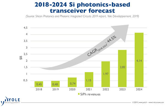
Figure 1. Silicon photonics 2013–2025 market forecast [1]. Reproduced with permission from S. Leroy, Director, Public Relations at Yole Développement.
This is because in the near future new technologies must be introduced. The research activity in Silicon photonics can be dated back to the 1980s and in recent years more and more players are emerging in this industry's landscape. Nowadays, Intel shares the leadership in this field with Luxtera, with products for 100 G data rates already present on the market. As Silicon (Si) is a mature technology developed during the years of the strong expansion of the microelectronic industry, the use of Si for the fabrications of photonic components meet the requirements of the data center in term of low cost, reliability, integration density and power consumption. A key component in Si photonics is constituted by the photodetectors (PDs), devices that are able to convert the incoming light into current.
Si PDs are commercial devices in the visible spectrum, however, the employment of Si for the realization of PD operating at near-infrared (NIR) wavelengths is not a simple task due to Si transparence above 1.1 μm. NIR Si PDs take conventionally advantage of germanium (Ge) integration [2][3] on Si, however, due to a 4.3% lattice mismatch, very high leakage current hinders the device performance. This issue can be mitigated by realizing a buffer layer based on a two-step epitaxial growth technique [2][3] that minimize but, unfortunately, do not remove the defect center responsible of the high leakage current. Moreover, this buffer layer generates some problems in terms of thermal budget and planarity [4] preventing the possibility of a monolithic Ge integration on Si. In addition, Ge is characterized by a low absorption at 1550 nm with respect to gallium arsenide (InGaAs) leading to thick active intrinsic region of the PIN structures and slow devices.
2. Theoretical Background
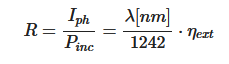
In order to quantify the performance of IPE-based PDs, a very important parameter is the internal quantum efficiency ηint, i.e., the ratio of the number of charge carriers generated by the PD to the number of absorbed photons. On the other hand, the external quantum efficiency ηext (the ratio of the number of charge carriers generated by the PD to the number of incident photons) is linked to the internal by ηext = A ηint, being A the active material absorption. A macroscopic magnitude is the responsivity R, i.e., the ratio of the photogenerated current (Iph) to the incident optical power (Pinc). The responsivity R is linked to the external quantum efficiency ηext by the following:
3. IPE-Based Silicon Photodetectors Based on Graphene Schottky Junctions
Since its discovery in 2004, graphene has been deeply investigated [5]. Indeed, electrons move in graphene as massless particles making it suitable for fast electronics, while the wide absorption (from UV to IR) due to both intra-band and inter-band transitions [6][7] makes the material very useful in the photodetection field in particular for operation at NIR wavelengths. In 2011, Chen et al. demonstrated that graphene is able to form a Schottky junction with Si [8] and this result opened the path to the investigation of IPE in the graphene/silicon junctions for NIR detection.
NIR vertically illuminated IPE-based graphene/Si PDs were reported by Amirmazlaghani et al. in 2013 [9]. These devices are based on exfoliated graphene and show a 9.9 mA/W maximum responsivity at 1550 nm and −16 V of reverse bias applied. Indeed, as shown in Figure 2b, the difference between the photogenerated and dark current is about 51.5 nA under 5.2 μW.
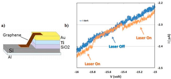
Figure 2. (a) Sketch describing the graphene-silicon (Si) Schottky diode investigated in Amirmazlaghani [9]. (b) The current-voltage I-V curve at reverse bias (from −16 to −15 V). This figure demonstrates the change in diode current by switching on and off the laser at 1550 nm. Reprinted with permission from (Amirmazlaghani, Raissi, Habibpour, Vukusic, Stake. Graphene-Si Schottky IR detector. IEEE J. Quant. Elect. 2013, 49, 2589). Copyright (2013) IEEE.
In addition, a 2.4 μA of dark current was measured while an SBH and ideality factor of 0.44–0.47 eV and 1.3–2.1 were extracted from the IV Schottky characteristic, respectively. In this paper, the authors point out the measured responsivity is much higher than that one estimated by Equation (2). This discrepancy has been explained by claiming that a new IPE theory must be derived when 2D materials are involved in the junction. Indeed, they derived a modified model (Equation (5)) for a better prediction with the experimental data. It is worth mentioning that Levy at al. have recently discussed and explained the physics behind the IPE enhancement in junctions involving 2D materials [10]. Subsequently, Goykhman et al. reported on a near-infrared graphene/Si Schottky PD integrated with a waveguide realized starting from a silicon-on-insulator (SOI) substrate. In this device the single graphene layer (SLG) is grown by chemical vapor deposition CVD system [11] (Figure 3).
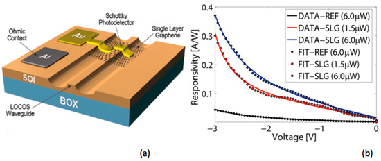
Figure 3. (a) Scketch of the Graphene/Si Schottky photodetectors (PD) investigated in Goykhman [11]. (b) Responsivity of Graphene/Si Schottky PDs and Metal−Si PDs (for comparison). Solid lines are the curve fitting obtained by taking into account a combined avalanche multiplication and thermo field emission effect. Reprinted with permission from (Goykhman, Sassi, Desiatov, Mazurski, Milana, de Fazio, Eiden, Khurgin, Shappir, Levy, Ferrari. Integrated, Silicon–Graphene Plasmonic Schottky Photodetector with High Responsivity and Avalanche Photogain. Nano Lett. 2016, 16, 3005–3013. Direct link: https://pubs.acs.org/doi/10.1021/acs.nanolett.5b05216). Copyright (2016) American Chemical Society. Further permissions related to the material excerpted should be directed to the ACS.
The PD is constituted by a Si rib waveguide on which a SLG/Au layer acting as Schottky contact has been deposited. The collecting Ohmic contact is realized in aluminum (Al) and deposited on the Si substrate as shown on Figure 3a. The optical beam propagating along the Si waveguide is able to excite the plasmonic modes at SLG/Si interface. The photodetector length and width are ~5 μm and 310 nm, respectively. At 1 V of reverse bias applied, a responsivity at 1550 nm and dark current of 0.085 A/W and 20 nA were experimentally measured. Finally, the authors show that responsivity abruptly increases up to 0.37 A/W at −3 V. The authors explain this abrupt increase by the combined effect of two processes: avalanche multiplication within the Si depletion region and thermionic-field emission (TFE) [12] through the graphene/Si Schottky junction. Under avalanche conditions, the dark current also increases up to 3 μA. The SBH extracted by the electrical measurement is 0.34 eV.
More recently, in 2017, Casalino et al. have reported on vertically-illuminated graphene/Si Schottky PDs incorporated into a Fabry-Perot optical microcavity [13]. The resonant cavity consists of a λ/2 Si slab layer surrounded between graphene/Si top and Au bottom mirrors as shown in Figure 4a. The optical cavity is able to enhance the interaction of the light with graphene in order to increase its absorption. In this work, the authors prove that the device responsivity peaks coincide with the resonances of the Fabry-Perot microcavity and that the responsivity increases with the number of light round trips of the cavity. Thanks to the multiple reflections in the cavity, the graphene absorption increases up to 8% leading to a maximum responsivity increasing with the reverse voltage applied and reaching a maximum of ~20 mA/W at −10 V (Figure 4b); this value is the highest reported so far for free-space illuminated Si PDs at 1550 nm. In addition, the authors prove the SBH dependence on applied reverse voltage. Finally, the dark current at −10 V has been measured as 147 μA while the device bandwidth has been estimated in 120 MHz.

Figure 4. (a) Optical image of fabricated device investigated in Casalino [13]. (b) Responsivity vs reverse voltage. Reprinted with permission from (Casalino, Sassi, Goykhman, Eiden, Lidorikis, Milana, De Fazio, Tomarchio, Iodice, Coppola et al. Vertically Illuminated, Resonant Cavity Enhanced, Graphene-Silicon Schottky Photodetectors. ACS Nano 2017, 11, 10955–10963). Copyright (2017) American Chemical Society.
In order to increase the low graphene absorption of the previous device (only 8%), the same author has theoretically proposed a resonant cavity-enhanced (RCE) graphene/Si PD working at 1550 nm based on IPE [14]. Device is essentially a Fabry–Perot interferometer constituted by three layers of crystalline Si, graphene and hydrogenated amorphous Si surrounded by two high-reflectivity Bragg mirrors as shown in Figure 5a. The optical field enhancement allows increasing the single-layer graphene optical absorption up to 100%. The optoelectronic transduction mechanism is based on IPE where the photoexcited carriers are emitted from graphene to Si. In this work, it has been theoretically proved that an optimized device can reach an external quantum efficiency of 35% and responsivity of 0.43 A/W, as shown in Figure 5b. Finally, device speed and noise, have been discussed.
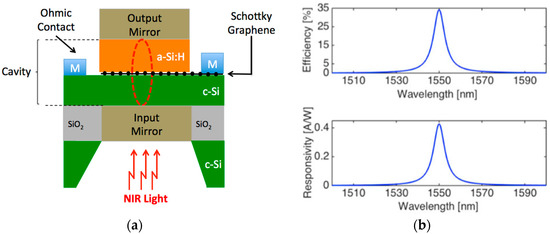
Figure 5. (a) Section sketch and (b) theoretical responsivity and quantum efficiency of the high-finesse resonant cavity enhanced PD investigated in Casalino [14]. Reprinted with permission from (Casalino. Design of Resonant Cavity-Enhanced Schottky Graphene/Silicon Photodetectors at 1550 nm. J. Ligthwave Technol. 2018, 36, 1766–1774). Copyright (2018) IEEE.
Very recently this family of devices have demonstrated the capability to work also at wavelengths longer than 1550 nm [15]. Indeed, in the Casalino's work [15] vertically-illuminated silicon PD operating at 2 µm has been reported. The sketch of the device is shown in Figure 6a; it is a graphene/silicon Schottky junctions whose electrical parameters are carefully extracted at various temperature increasing from 280 to 315 K. The Schottky barrier is 0.62 eV at 300 K and shows a dependence on temperature ascribed to interface defects. Devices show a responsivity of 0.16 mA/W (Figure 6b) at zero bias. It corresponds to internal responsivities of at least 7.2 mA/W. Measured dark current is ~3 μA at −6 V while the estimated bandwidth is in the KHz range due to the very high series resistance. The proposed devices show the potentialities to work also at wavelength longer than 2 micron.
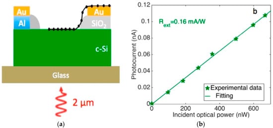
Figure 6. (a) Schematic cross-sectional view of the graphene/Si Schottky PD investigated in Casalino [15], (b) Measured current vs incident optical radiation. Reprinted with permission from (Casalino, Russo, Russo, Ciajolo, Di Gennaro, Iodice, Coppola. Free-Space Schottky Graphene/Silicon Photodetectors operating at 2 μm. ACS Photonics 2018, 5, 4577–4585. Copyright (2018) American Chemical Society.
4. Conclusions
In this work an overview of near-infrared Si PDs based on IPE occurring in graphene, has been presented. Firstly, we have described how IPE theory needs to be properly modified in junctions involving two-dimensional material, showing as this effect is intrinsically enhanced with respect to classical device based on 3D materials (metals). Then we have described and discussed in detail the most common configurations reported in recent literature including both vertically-illuminated and waveguide structures.
In some cases, this new family of devices shows performance that is already comparable to PDs based on Ge technology utilized in Si photonics for both telecom and datacom applications. In addition, these devices show the potentialities for working at longer wavelengths opening perspectives for new applications including optical communications, light-radars and biomedical imaging. However, the possibility to integrate 2D materials like graphene in Si technology for high-volume production remains a crucial point that needs to be properly addressed in the next future.
This entry is adapted from the peer-reviewed paper 10.3390/app9183677
References
- Yole Dèvelop. Available online: https://www.i-micronews.com/category-listing/product/silicon-photonics-2018.html (accessed on 28 June 2019).
- Koester, S.J.; Schaub, J.D.; Dehlinger, G.; Chu, J.O. Germanium-on-SOI infrared detectors for integrated photonic applications. IEEE J. Sel. Top. Quantum Electron. 2006, 12, 1489–1502.
- Harame, D.L.; Koester, S.J.; Freeman, G.; Cottrel, P.; Rim, K.; Dehlinger, G.; Ahlgren, D.; Dunn, J.S.; Greenberg, D.; Joseph, A.; et al. The revolution in SiGe: Impact on device electronics. Appl. Surf. Sci. 2004, 224, 9–17.
- Wang, J.; Lee, S. Ge-Photodetectors for Si-Based Optoelectronic Integration. Sensors 2011, 11, 696–718.
- Novoselov, K.S.; Fal’ko, V.I.; Colombo, L.; Gellert, P.R.; Schwab, M.G.; Kim, K. A roadmap for graphene. Nature 2012, 490, 192–200.
- Dawlaty, J.; Shivaraman, S.; Strait, J.; George, P.; Chandrashekhar, M.; Rana, F.; Spencer, M.G.; Veksler, D.; Chen, Y. Measurement of the optical absorption spectra of epitaxial graphene from terahertz to visible. Appl. Phys. Lett. 2008, 93, 131905.
- Sensale-Rodriguez, B.; Yan, R.; Kelly, M.M.; Fang, T.; Tahy, K.; Hwang, W.S.; Jena, D.; Liu, L.; Xing, H.G. Efficient terahertz electro-absorption modulation employing graphene plasmonic structures. Appl. Phys. Lett. 2012, 101, 261115.
- Chen, C.-C.; Aykol, M.; Chang, C.-C.; Levi, A.F.J.; Cronin, S.B. Graphene-silicon Schottky diodes. Nano Lett. 2011, 11, 1863–1867.
- Amirmazlaghani, M.; Raissi, F.; Habibpour, O.; Vukusic, J.; Stake, J. Graphene-Si Schottky IR detector. IEEE J. Quant. Elect. 2013, 49, 2589.
- Levy, U.; Grajower, M.; Goncalves, P.A.D.; Mortensen, N.A.; Khurgin, J.B. Plasmonic silicon Schottky photodetectors: The physics behind graphene enhanced internal photoemission. APL Photonics 2017, 2, 26103.
- Goykhman, I.; Sassi, U.; Desiatov, B.; Mazurski, N.; Milana, S.; De Fazio, D.; Eiden, A.; Khurgin, J.; Shappir, J.; Levy, U.; et al. On-Chip Integrated, Silicon–Graphene Plasmonic Schottky Photodetector with High Responsivity and Avalanche Photogain. Nano Lett. 2016, 16, 3005–3013.
- Padovani, F.A.; Stratton, R. Field and thermionic-field emission in Schottky barriers. Solid State Electron. 1966, 9, 695–707.
- Casalino, M.; Sassi, U.; Goykhman, I.; Eiden, A.; Lidorikis, E.; Milana, S.; De Fazio, D.; Tomarchio, F.; Iodice, M.; Coppola, G.; et al. Vertically Illuminated, Resonant Cavity Enhanced, Graphene-Silicon Schottky Photodetectors. ACS Nano 2017, 11, 10955–10963.
- Casalino, M. Design of Resonant Cavity-Enhanced Schottky Graphene/Silicon Photodetectors at 1550 nm. J. Ligthwave Technol. 2018, 36, 1766–1774.
- Casalino, M.; Russo, R.; Russo, C.; Ciajolo, A.; Di Gennaro, E.; Iodice, M. Free-Space Schottky Graphene/Silicon Photodetectors operating at 2 μm. ACS Photonics 2018, 5, 4577–4585.