A coordinate measuring machine (CMM) is a measuring instrument that can measure three-dimensional (3D) shapes of an object, including a probing system to detect an object’s surface, a positioning stage system to move either the probing system or the object, length scales to determine the coordinate of detected points by the probing system, as well as software to control the entire measurement. Micro-coordinate measuring machines (micro-CMMs) for measuring microcomponents require a probe system with a probe tip diameter of several tens to several hundreds of micrometers. Scale effects work for such a small probe tip, i.e., the probe tip tends to stick on the measurement surface via surface adhesion forces. These surface adhesion forces significantly deteriorate probing resolution or repeatability.
1. Introduction
A coordinate measuring machine (CMM) is a measuring instrument that can measure three-dimensional (3D) shapes of an object, including a probing system to detect an object’s surface, a positioning stage system to move either the probing system or the object, length scales to determine the coordinate of detected points by the probing system, as well as software to control the entire measurement [
1]. Although X-ray-computed tomography has recently been developed [
2,
3], CMMs are still the most reliable measurement system for evaluating object shapes, dimensions, postures, and positions. Therefore, CMMs are generally used in industry as standard measurement systems [
4]. However, manufacturing technologies have significantly developed to produce miniature parts, including small-scale shapes or components such as microgears, inkjet nozzles, and microholes [
5,
6,
7,
8,
9]. Therefore, CMMs with nanoscale accuracy have been in high demand for evaluating the dimensions and shapes of these micro-scaled products. Takamasu et al. proposed the concept of a nano-CMM in 1996 [
10]. Furthermore, other researchers, institutes, and companies have addressed the development of micro-/nano-CMMs [
11,
12,
13,
14,
15,
16,
17,
18]. Although there are different concepts for highly accurate CMMs, the representative specifications shown in
Table 1 are important for micro-CMMs. Many names for CMMs with nanoscale accuracy have been proposed; however, herein, the term “micro-CMM” is used. The required specifications of micro-CMMs are approximately one-hundredth of the size of conventional CMMs (
Table 1), which is a significant challenge to achieve. Currently, micro-CMMs are commercially available, as summarized in [
19]. The positioning system and scale must achieve high accuracy (
Table 1). Most conventional CMMs do not meet the Abbe principle; however, for micro-CMMs, Abbe error-free structures are required to meet high accuracy. To meet the Abbe principle, metrology frames with interferometers are often used [
20,
21,
22,
23,
24].
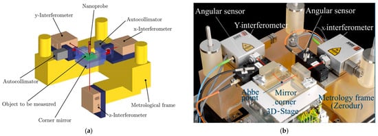
Figure 1a shows an Abbe error-free structure design example. The three laser interferometers for the X-, Y- and Z-axes are aligned to the probe tip of the probe system and measure the displacement of the metrology frame. In addition to the Abbe error, thermal drift is an important factor for reducing measurement uncertainty of the micro-CMMs. Therefore, in the micro-CMM structure, low thermal expansion materials such as Zerodur
® and Inver
TM were used (
Figure 1b) [
11,
22,
23]. Moreover, it is important to separate heat sources. In the example of
Figure 1, a stabilized He–Ne laser was isolated. For micro-CMMs, not only were these proposed, but many other intelligent designs to minimize the measurement uncertainty of the positioning stage have been presented. Consequently, the positioning stage achieved remarkably low uncertainty of as small as 50 nm or less [
25,
26]. The positioning stage shown in
Figure 1 is the highly precise positioning system developed by Jager and Manske [
25], which is now commonly used for micro-coordinate metrology. This intelligent system has a working range of 25 × 25 × 5 mm
3 and sub-nanometer stability.
Figure 1. Nano-positioning system, reprinted with permission from ref. [
25]. Copyright 2012 IOP Publishing: (
a) conceptual sketch of the nano-positioning system; (
b) photograph of the positioning stage system.
Table 1. The required specifications of micro-CMMs in [
10].
| |
Conventional CMM
|
micro-CMM
|
|
Measuring range
|
(1 m)3
|
(10 mm)3
|
|
Resolution
|
1 μm
|
10 nm
|
|
Accuracy
|
5 μm
|
50 nm
|
|
Probe tip size
|
5 mm
|
50 μm
|
|
Measuring force
|
10−1 N
|
10−3 N
|
In terms of micro-CMMs, probe systems [
9,
26,
27] are difficult to establish. The probe system with conventional CMMs performed excellently, with a repeatability of several tens of nanometers. However, as a microprobe system, its probe system structure is difficult to use. The probe system for micro-CMMs must be miniaturized (
Table 1). Conventional touch-trigger probe mechanisms are no longer adequate for probe systems of micro-CMMs (microprobe system) because of the scale effect. Generally, the probe tip makes contact with the surface of the objects to detect their surface. At the microscale, this conventional mechanism may not function properly. This is because the dominant force acting on the probe tip transitions from volume forces such as gravity to surface forces such as adhesion forces. Therefore, probe tips tend to stick to the surface, thus degrading the detection repeatability. The measuring force is another reason. Even when the measuring force is reduced, the contact pressure remains relatively high, which causes surface damage. Because of these effects, it is difficult to use conventional mechanisms of the touch-trigger probe. Therefore, to date, different types of probe systems have been proposed. The proposed microprobe systems were well summarized in several review studies [
28,
29,
30]. The overall probe systems for coordinate metrology, including conventional and microprobe systems, were summarized in [
28]. Ref. [
29] describes early-stage microprobe systems developed in the early 2000s. Many microprobe systems have been developed to date; they are classified in two types: contact probes, which have a mechanism that can detect contact with high sensitivity; and probes that use the interaction between the probe tip and measurement surface to detect the measurement surface. Ref. [
30] specifically focuses on summarizing the former type of the microprobe system. For the latter microprobe system, various types of probe systems using near-field physical phenomena acting on the probe tip and measurement surface have been proposed. Multiple unconventional surface-sensing principles that use physical interaction phenomena with the measurement surface rather than physical contact have been proposed, and their potentials have been explored.
2. Overview of Microprobe System for Coordinate Metrology
2.1. Issues for Microprobe System
This section discusses factors that must be considered when developing a microprobe system for micro-CMMs. First, the most different specification is the size of the probe tip. The size of the probe tip in CMM measurements directly affects the measurement’s accessibility; therefore, a small probe tip is required for micro-CMMs. Conventional probe systems have probe tips as large as millimeter-scale in diameter; typically, several millimeters. However, the microprobe systems require a few hundred to several dozens of micrometers in diameter (Table 1), i.e., the size of the probe tip must be reduced to one-fiftieth to the hundredth of the conventional probe tip. Due to the scale effect, the physical phenomena which contribute to the microprobe tip differ from conventional probes at the microscale. As a result of this disparity in a dominant physical phenomenon, various effects of these different physical phenomena should be considered.
Surface forces vary significantly depending on the material, surface properties, and environment.
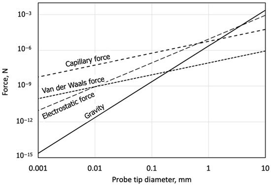
Figure 2 shows the surface forces working on the microprobe tip. The surface forces become increasingly more prominent than gravity when the size of the microprobe tip is less than a few millimeters. Surface forces are several orders of magnitude greater than gravity at scales of several tens to several hundred micrometers in diameter [
31,
32,
33,
34]. Therefore, surface forces attract the probe tip to the surface when the probe tip is close to the measurement surface [
35]. Although surface forces can be reduced via chemical treatment, surface texture, and environmental control [
32,
33], it is difficult to ignore the effect of these surface forces in micro-CMM probes. Surface forces significantly degrade measurement repeatability and reproducibility. Moreover, these surface forces cause probe tips to stick to the measurement surface and vibrate. The smaller the probe diameter, the more remarkable these effects become. In certain cases, increasing the probe stiffness solves the problem; moreover, another approach to avoid the sticking problem is to use non-contact or semi-contact detection. Furthermore, when the probe tip comes into contact with the measurement surface, the strong adhesion forces can induce contamination on the probe tip and measurement surface [
36]. Moreover, there is a technique of scanning measurement using this probe tip sticking. The probe tip and measurement surface are in contact using a flexible probe system with low stiffness, such as optical fiber, and the probe tip is scanned over the measurement surface [
37].
Figure 2. Surface forces working on the microprobe tip with dependence on the tip diameter. The calculation equations for each force are based on [
32]. The probe tip and measurement surface material were assumed to be tungsten carbide and silicon, respectively. The distance between the probe tip and measurement surface was assumed to be 10 nm. Other parameters were as follows: the surface tension was 72.5 mN/m, the contact angle was 75°, the permeability in a vacuum was 8.85 × 10
−12 F/m, the relative permittivity was 12, the charge density was 10 µC/m
3, the contact potential was 1 V, and the ratio of Young’s yield and Poisson’ ratio was 1.86 × 10
−12 m
2/kg.
Furthermore, there is an effect of measuring force on the microscale measurement. A large measuring force can damage the measurement surface [
38]; therefore, the probing force is one of the important specifications. A large measuring force induces other influences such as probe tip wear during scanning measurement [
39,
40]. The measuring force must be considered in terms of stress, e.g., if the probe tip diameter is reduced to 1/10, the contact area will be reduced to 1/100, thus resulting in 100 times more stress on the measurement surface. Therefore, for micro-CMM measurements, a significant small measuring force (
Table 1) is required [
41]. Theoretically, Hertzian’s equation is commonly used to consider the effect of the spherical probe contacting the measurement surface.
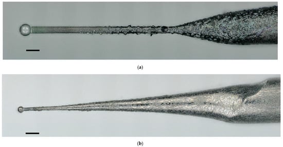
For microprobe systems, it is difficult to process microprobes and assemble microprobe systems [
42,
43]. Probes require dimensions which are less than a few hundred nanometers; therefore, it is difficult to process measurements with high precision because the probe tip requires high sphericity. Moreover, the aspect ratio of the probe system must be sufficient. When the probe size is several tens of micrometers, a thinner probe shaft is required, and high stiffness is difficult to design. The processing methods for manufacturing the microprobe tip have been examined. The proposed methods are classified into two categories [
44,
45]: the first is to attach a spherical probe tip to a shaft (
Figure 3a), whereas the second is to melt the probe shaft end or fabricate the probe tip (
Figure 3b). High-sphericity microspheres are commercially available; thus, they can be processed by gluing them to the probe tip [
45,
46,
47,
48]. Although this is possible at a laboratory scale, it is difficult to maintain high yield and low processing costs when considering commercial applications. In terms of the method of melting or fabricating the tip [
37,
45,
46,
49,
50,
51], the diameter, sphericity, and surface texture depend on processing conditions, thus requiring a stable processing technology. Here, the probe tip’s dimensions, shape, and surface texture must be measured. Although multiple measurement techniques have been proposed [
52], a method that can be used precisely on machines has yet to be established, and future research is expected.
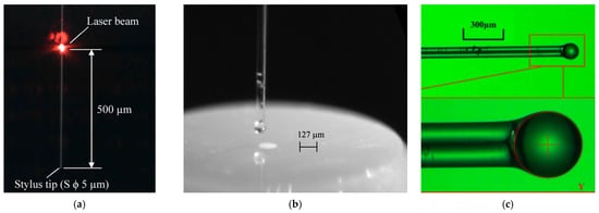
Figure 3. Images of microprobe tip fabricated by wire-electro-discharge grinding (WEDG) [
50]. The black bar indicates 100 μm: (
a) Glass tip attached at the end of the shaft. The diameter of the tip was 70 μm; (
b) Tungsten carbide tip. The diameter of the tip was 59 μm.
To ensure the measurement uncertainty of micro-CMMs, the evaluation of microprobe system technology is required. Probe tip diameter, probe tip shape, axial misalignment between probe shaft and probe tip, and other parameters are required for the evaluation. If the measurement accuracy of micro-CMMs is supposed to be 50 nm, the diameter and shape should be measured as accurately as ~10 nm or less. Many techniques for measuring probe diameter and shape have been proposed [
52,
53,
54,
55,
56,
57,
58,
59,
60,
61,
62]; however, few are accurate to 10 nm; Meli et al. achieved a repeatability of 4 nm using two spheres and the probe tip [
59,
60]. This method has excellent repeatability and potential; however, the calibration process includes the traceability route, and therefore, a more straightforward on-machine measurement method is preferred.
Pre-travel is known to be an important parameter for microprobe systems. Generally, the faster the probe approaches the measurement surface, the better it is for reducing the total measurement time. However, if the rapid approach speed causes the probe tip to considerably over-travel after contact with the measurement surface, the measurement object or the microprobe system can be damaged. Therefore, microprobe systems must have a long pre-travel. If the pre-travel time is reduced, the probe system approach must be stopped as soon as possible after detection. Therefore, to reduce inertia, the dynamic mass of microprobe systems or positioning stages must be as small as possible.
2.2. Contact Probing System with Hinge Structure
Microprobe system development began in the early years at NMIs and universities in Europe and the United States, as well as Japan [
11,
47,
59,
63,
64,
65,
66,
67,
68,
69], where many types of probe systems were developed. In particular, there have been developments of microprobe systems with relatively large probe tip sizes and high sensitivity, in which a hinge structure is used to detect the contact between the probe tip and measurement surface [
59,
63,
64,
67].
Figure 4 shows certain examples of hinge-typed microprobe systems. The primary point of this probe type is to measure the deformation of the hinge with high sensitivity; therefore, multiple methods, such as optical measurement [
60], capacitive sensors [
22,
60], and silicon membrane sensors [
64] have been proposed. This hinge-type probe system has been proposed and developed [
70,
71,
72,
73,
74,
75,
76,
77,
78,
79,
80,
81,
82,
83,
84,
85,
86], and certain commercially available microprobe systems of this type are available [
87,
88,
89,
90,
91,
92]. By designing structures and materials, hinge-type probe systems can control the stiffness of the probing system. Therefore, the high detection sensitivity could be designed, and multiple probes have achieved resolutions of several nanometers [
59,
93,
94,
95]. Furthermore, hinge-type microprobe systems can be designed to be compact to reduce the dynamic mass [
96]. The disadvantage is that the microprobe system is increasingly challenging to assemble compared with other types of probes introduced below; moreover, the pre-travel is typically limited, thus increasing concerns about damage to the microprobe system. Therefore, probes that are easy to replace are expected [
96]. Probes that incorporate piezoelectric actuators in the hinge to make the probe tip actively vibrate by stretching and contracting is an interesting example of a hinge-type probe [
97,
98]. There is a probe that can change the stiffness of the hinge structure [
99]. The low measurement force and 3D isotropy of sensing could be achieved by designing an intelligent hinge structure [
59,
96]. Furthermore, using MEMS, a probe system that can be oscillated in three axes and incorporates a three-axis electrostatic actuator has been proposed [
100]. Thus, the hinge-typed microprobe system can perform various functions by combining MEMS and semiconductor technologies and developing a hinge mechanism.
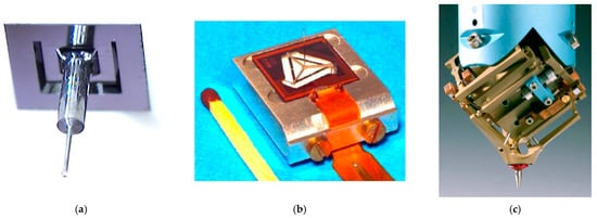
Figure 4. Example of hinge-typed microprobe systems: (
a) PTB [
64]; (
b) Eindhoven University, reprinted with permission from ref. [
63]. Copyright 2001 Elsevier, License Number: 5158820240105; (
c) Metas, reprinted with permission from ref. [
59]. Copyright 2007 IOP Publishing.
The use of the optical fiber has been proposed as a different approach [
101,
102,
103,
104,
105,
106,
107,
108,
109,
110,
111,
112,
113].
Figure 5 shows some of the examples. The diameter of the single-mode optical bare fiber was 125 μm, which is appropriate for the probe shaft; moreover, the probe tip can be made by melting the optical fiber tip. Multiple optical fiber-based microprobe systems have been proposed. For using an optical fiber, the contact of the probe tip to the measured surface is detected by measuring the deflection of the optical fiber stem using the optical method; furthermore, high resolutions are expected for this detection. The probe deflection can be measured with high resolution; however, the reproducibility of detection is difficult to improve. Furthermore, detection in the 2D direction perpendicular to the optical fiber has a relatively high resolution [
44,
92], whereas detection in the axial direction is difficult [
11,
97]. This optical fiber-type probe can be used for scanning measurement [
37]. Furthermore, there are examples of significantly small optical fiber probe tips that are smaller than several dozens of micrometers [
45,
94] because of the ease to make a smaller sphere by sharpening the fiber. Chemical treatment can be used to make a surface hydrophobic; however, there are certain disadvantages. The size of the microprobe system is larger than the abovementioned hinge-type probe because of the optical system [
109,
110]. Fiber Bragg gratings in an optical fiber can be used to detect the deflection of the fiber as an optical spectrum signal [
78,
101,
102]; furthermore, the use of multiple fibers to simultaneously measure the position and detection direction [
104,
112] are two interesting examples.
Figure 5. Examples of optical-fiber-based microprobe systems: (
a) University of Kitakyushu [
105]; (
b) NIST [
106]. (
c) Harbin Institute of Technology, reprinted with permission from ref. [
104]. Copyright 2013 Elsevier, License Number: 5158821208344.
Probe systems using physical interactions between the probe tip and measurement surface have been proposed as an alternative approach to the abovementioned hinge-type and fiber-based probe systems. As previously reported, it is necessary to avoid adhesion forces to reduce the probe tip size. Therefore, contact of the probe tip with the surface is avoided as much as possible, i.e., the surface is detected by measuring the physical quantity working on the probe tip and the measurement surface before contact. This probe detection principle is similar to that of scanning probe microscopy (SPM) probes and has excellent potential. Chapter 3 discusses the details of these types of probes.
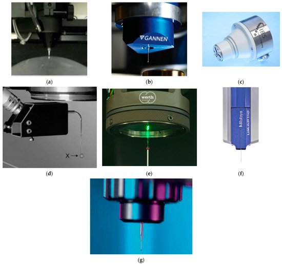
Finally, commercially available microprobe systems are summarized in Table 2 and Figure 6. Note that different types of probe principles have been commercialized. The probe tip size ranges from tens to hundreds of microns. The fiber probe has a particularly high aspect ratio and low contact force. Vibration probes have the same low probing force as fiber probes and a relatively high aspect ratio.
Figure 6. Commercialized microprobe systems: (
a) Panasonic, UA3P AFP [
114]; (
b) Xpress PE, GANNEN XP [
87]; (
c) IBS P.E. Trislelion [
89]; (
d) Werth Fiber Probe, WFP/S, reprinted with permission from ref. [
110]. Copyright 2012 Elsevier, License Number: 5158821452309; (
e) 3D Werth Fiber Probe [
107]; (
f) Mitutoyo, UMAP; and (
g) Zeiss, F25 probe, reprinted with permission from ref. [
90]. Copyright 2012 Elsevier, License Number: 5158830075542.
Table 2. Summary of the commercialized microprobe systems.
| |
Sensing Principle
|
Probe Tip Diameter
|
Shaft Length
|
Probing Force
|
Probe Tip Material
|
|
Panasonic, UA3P-AFP
|
Contact, Hinge-type probe
|
30, 80 μm
|
300, 500 μm
|
0.3 mN
|
Ruby, Tungsten carbide
|
|
Xpress PE, GANNEN XP
|
Contact, Hinge-type Vibration probe
|
50–120 μm
|
6.8 mm
|
0.4 mN
|
Ruby
|
|
IBS P.E. Trislelion
|
Contact, Hinge-type probe
|
80–250 μm
|
6–8.5 mm
|
0.3 mN
|
Ruby
|
|
3D Werth Fiber Probe
|
Contact, Fiber probe
|
40–250 μm
|
20 mm
|
1–100 μN
|
Glass
|
|
Werth Fiber Probe, WFP/S
|
Contact, Fiber probe
|
down to 25 μm
|
150 mm
|
1–100 μN
|
Glass
|
|
Mitutoyo, UMAP
|
Vibration probe
|
15–300 μm
|
0.2–16 mm
|
1–25 μN
|
Glass
|
|
Zeiss, F25 probe
|
Contact, Hinge-type probe
|
100–700 μm
|
up to 4 mm
|
0.5 mN
|
Ruby
|
2.3. Review the Specification of the Proposed Microprobe System
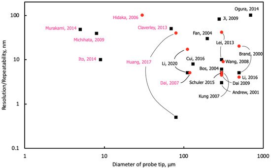
Many probes have been proposed to date. This section provides an overview of microprobe systems based on their specifications. As previously reported, there is a close relationship between probe tip size and performance. Therefore, the discussion was developed based on the probe tip size. Figure 7 shows the relationship between the probe tip size and resolution or repeatability of researchers’ proposed microprobe systems. The black squares and red circular plots show the resolution and repeatability of the microprobe system, respectively. The plots are denoted name and year. Those with black and red font show the contact-type and physical interaction probes. The evaluation criteria differ among studies; thus, the purpose of Figure 7 is not to rank the performance of microprobe systems, but to overlook the trend based on the probe tip size and probing principle.
Figure 7. Resolution and repeatability of the proposed microprobe system.
First, the figure shows that the common probe tip size of microprobe systems for micro-CMMs is several hundred micrometers, although certain microprobe systems have been proposed to be a few tens of micrometers, or even smaller. The tendency in
Figure 7 shows that the larger the probe tip size, the more likely a higher resolution can be achieved. This is because of the influence of adhesion forces and other previously mentioned factors. For probes with a tip diameter of >100 μm, the dominant force is close to the volume force; therefore, the effect of adhesion force is small, resulting in a high resolution or repeatability of <10 nm. However,
Figure 7 shows that when the probe tip size is less than several tens of micrometers, obtaining a resolution greater than 10 nm becomes difficult. The contact-type microprobes are designed for high-resolution and a relatively large probe diameters of several hundred micrometers. The tip diameters of physical interaction probes seem smaller. The physical interaction probes use various physical phenomena to detect surfaces. However, it is difficult to achieve a resolution of 10 nm or repeatability. Furthermore, Ito et al. [
115] and Huang et al. [
116] proposed the principle of share force detection, which has demonstrated a high potential to achieve single-nano resolution.
This entry is adapted from the peer-reviewed paper 10.3390/metrology2010004