Your browser does not fully support modern features. Please upgrade for a smoother experience.
Please note this is an old version of this entry, which may differ significantly from the current revision.
Subjects:
Physics, Applied
Forevacuum plasma electron sources, operating at elevated pressure values from units to hundreds of pascals, make it possible to exert the direct action of an electron beam on low-conductive materials. Electron-beam evaporation of aluminum oxide, boron, and silicon carbide targets is used to exemplify the particular features of electron-beam synthesis of such coatings and their parameters and characteristics.
- thin films deposition
- laser deposition
- electron-beam deposition
- magnetron sputtering
- fore-vacuum plasma electron sources
1. Introduction
Dielectric coatings based on oxides, nitrides, borides, carbides, and other compounds take up a special place among various functional and protective thin-film coatings. Such coatings are normally characterized by high hardness, temperature, and corrosion resistance, with the majority of them being electrically insulating [1]. Ceramic coatings, deposited onto the metal surfaces, are used to protect them from thermal and mechanical damage, corrosion, and premature wear. Such coatings are widely used in the automotive and aerospace industries, nuclear energy, and medicine. For the first time, ceramic coatings have begun to be used in the aerospace industry for covering the gas turbine engine blades exposed to increased corrosive and erosive wear due to constant temperature changes. In the nuclear energy industry, they are used to cover the elements of the reactors, cooling systems, and nuclear fuel storages. In the military-industrial complex, ceramic compounds are used to cover equipment cases, weapon elements, and special products. The coatings used in metalworking increase the hardness and lifetime of the parts. In the automotive industry, ceramic materials are used to protect components of engines, rims, and chassis; in medicine, they are used to protect devices and parts of prostheses. Thin boron-containing films (pure boron, boron carbide, or nitride) are widely used in microelectronics, nuclear power, and aerospace due to their high hardness, strength, wear resistance, chemical inertness, and dielectric properties, as well as the ability of boron to absorb neutron radiation.
For many industrial applications, it is desirable for the coatings to combine these properties at a relatively low production cost. For example, aluminum oxide, the most commonly used dielectric in virtually all industries, is a chemically inert, corrosion-resistant material with a relatively low cost as compared with other ceramics. Its hardness (15–20 GPa) is on par with hard alloys and its specific resistance (1014 Ω·cm) with the best electrical insulating materials [2]. Coatings based on aluminum oxide can operate at temperatures up to 1500 °C and find wide applications in modern instrument and mechanical engineering [3]. Boron-based coatings, boron nitride and metal borides, are of considerable interest. These compounds are chemically inert, temperature resistant, and have high hardness. The hardness of cubic boron nitride surpasses that of diamond, and its decomposition temperature is twice as high as that of diamond [4]. Note that boron-containing surface layers are created today most often by using the filler brazing technology [5] or the more up-to-date technology of gas borating in the atmosphere of decomposing, usually toxic, gaseous boron compounds [6].
The search results for the keywords “dielectric coatings” in publications of the American Institute of Physics (AIP), Institute of Electrical and Electronic Engineers (IEEE), Institute of Physics (IOP), Elsevier, American Institute of Aeronautics and Astronautics (AIAA), and other institutions show a significant increase in the number of articles on this topic over the last five years (Figure 1).
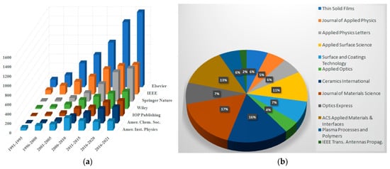
Figure 1. Publication dynamics on dielectric coatings and their breakdown by publishers (a), and the set of the journals publishing articles on “dielectric coatings” (b).
Beam-plasma methods of creating multifunctional dielectric coatings in vacuum or a rarefied gas, such as magnetron spattering, vacuum arc plasma deposition, laser ablation, electron-beam evaporation, and plasma-enhanced chemical methods, are used for addressing a wide range of practical problems related to surface modification of various materials. Among the extensive nomenclature of beam-plasma technologies, the electron-beam synthesis of coatings is characterized by a faster deposition rate and, hence, higher productivity [7]. Creation of dielectric coatings by electron-beam evaporation is hampered due to the electrical charging of the evaporated surface of the target. To neutralize the charging, it is necessary, at least at the initial stage of the technological process, to employ special methods and approaches [8] that complicate the equipment and diminish control over the process and its efficacy.
Forevacuum plasma electron sources are capable of generating electron beams in the previously inaccessible forevacuum range of elevated pressure (1–100 Pa). They have the same usual advantages of conventional plasma electron sources: high current density, reliability, they are non-sensitive to rough vacuum conditions and the presence of active gases. The plasma formed in the electron-beam transport region at an elevated pressure of the forevacuum range effectively neutralizes the surface charging of non-conductive materials by the electron beam [9]. This opens up a principal opportunity for using forevacuum plasma electron sources for electron-beam evaporation of dielectric materials and creating coatings [10]. Additionally, the beam plasma, generated in the forevacuum pressure range, can be used to provide ion-plasma assistance for electron-beam synthesis of dielectric coatings or modification of the surface properties of dielectric materials [11,12].
2. Synthesis of Dielectric Coatings using Forevacuum Plasma Electron Sources
2.1. Forevacuum Plasma Electron Sources: Basic Principles of Operation
The so-called forevacuum plasma electron sources represent a modern development trend of electron sources, based on the emission of electrons from the low-temperature plasma [101]. Sources of this type provide efficient generation of electron beams in the previously inaccessible range of elevated pressure from a few to over a hundred of pascal [102]. The move to the region of higher pressure values needs to consider the operation of discharge-emission plasma electron sources and solve a number of scientific and engineering problems related to the stable work of electron sources with the electron-beam parameters that are attractive for real-world applications.
Unlike for conventional plasma electron sources, for forevacuum plasma electron sources, it is virtually impossible to create a pressure drop between the region of the emission plasma generation and the beam formation regions. Besides, the parameter pd (p—pressure, d—the gap length) for the accelerating gap of forevacuum plasma electron sources is closer to the minimum of the Paschen curve, which significantly increases the probability of gap breakdown. Note also the fact that in the region of elevated forevacuum pressure, the effect of a parasitic high-voltage glow discharge in the accelerating gap and the back ion flux from the beam plasma on the generation of the electron beam is significantly stronger [103].
The problem of the stable generation of an electron beam by a forevacuum plasma electron source in the isobaric regime has been successfully solved by creating special conditions for effective synthesis of emission plasma in the discharge system and simultaneous suppression of ionization processes in the regions of electron acceleration and beam formation. Thus, to form focused continuous electron beams at an elevated pressure, which are most suitable for electron-beam evaporation of materials, forevacuum plasma electron sources make use of a hollow cathode glow discharge for generation of emission plasma [104]. Electrostatic confinement of electrons inside the cathode hollow provided, as a result of their multiple oscillations, a high rate of ionization and, consequently, a high electron emission current density from plasma. The use of plane-parallel accelerating gap, whose electrodes are placed at a minimal possible distance from each other, restricted ionization processes in the gap to a great degree and significantly increased its dielectric strength [101]. Additionally, to ensure a high dielectric strength of the accelerating gap, forevacuum plasma electron sources use specially designed accelerating systems [101] that inhibit the breakdown along the so-called “long paths” and diminish the effect of the back ion flux from the parasitic high-voltage glow discharge and beam plasma.
The electrode diagram of a forevacuum plasma source of a continuous electron beam based on a hollow cathode glow discharge [101] is shown in Figure 2.
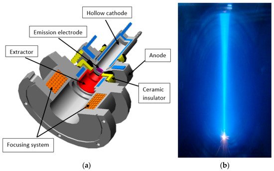
Figure 2. Electrode diagram of the electron source (a) and a photograph of the electron beam (b) [101].
The hollow cathode of the discharge system of the plasma electron source is made of stainless steel; its diameter is 15–30 mm and length 40–60 mm. The flat anode is also made of stainless steel. Electrons are extracted from the plasma through an emission window of a diameter of about 10 mm cut in the anode. To stabilize the plasma emission surface and ensure the stable operation of the electron source, the emission window is draped with a fine-structured tungsten grid with high geometric transparency, or a perforated tantalum electrode is used. The electron beam is focused by a magnetic lens.
In the operational pressure range of the forevacuum plasma electron source, a hollow cathode discharge current can amount to 1.0–1.5 A at a burning voltage of 500–600 V. As of today, maximal parameters of the forevacuum plasma electron source of a continuous focused electron beam based on a hollow cathode discharge are as follows [105,106]:
- -Accelerating voltage up to 30 kV;
- -Beam current up to 450 mA;
- -Beam power up to 10 kW;
- -Power density up to 106 W/cm2;
- -Operating pressure up to 100 Pa (argon), 160 Pa (helium).
The attained electron-beam parameters of the forevacuum plasma electron source are of almost the same level as those of conventional plasma electron sources that operate in the pressure range of one or two orders of magnitude lower than the forevacuum. This makes it possible to use electron sources of this type for thermal treatment of various materials. As will be shown below, forevacuum sources are unique in that they are capable of directly processing materials with low electrical conductivity; this includes melting and evaporation of high-temperature ceramics for the purpose of dielectric coating deposition.
2.2. Beam-Plasma Parameters and Characteristics
Low-temperature plasma finds a plethora of technological applications, such as plasma-chemical synthesis, coating deposition, modification of materials, sterilization of medical tools and instruments, etc. [107]. Plasma is usually generated in a certain type of gas discharge. To achieve the required plasma parameters in the gas discharge and be able to vary them within a wide range is quite a complicated task. This is due to the fact that the ionization processes in a gas discharge and the related steady-state plasma parameters, first of all, provide the stable burning of the discharge at a given current. Control over the plasma parameters by varying the discharge current is in many cases accompanied by a change in the discharge burning voltage, which determines the temperature of plasma electrons and thereby their ionization capacity. The burning voltage is also affected by the pressure and type of gas, by the presence of a magnetic field, and by a number of other factors. This all produces a disproportional influence of the current and external conditions of discharge burning on the discharge plasma parameters and thereby hinders the control over the plasma parameters.
Generation of plasma by an electron beam provides wider control over the plasma parameters. This is not only because the beam current and the accelerating voltage, which determines the electron energy, can be varied independently. It is fundamentally important that the beam-plasma parameters do not significantly affect the characteristics and parameters of the electron beam.
The maximum working pressure of conventional thermal emission or plasma cathode electron sources is limited by a level of 10−1 Pa [101]. At such a pressure, the possibilities of effective generation of beam plasma are limited. The move to the region of higher pressure requires creating special conditions for the pressure separation of the regions of the electron-beam formation and transport.
The advent and development of the so-called forevacuum plasma electron sources [101] that can form stable beams at a pressure of 1–100 Pa in an atmosphere of various gases, including chemically active oxygen, nitrogen, and others, made it possible to effectively generate a beam plasma and use it for ion-plasma surface modification of various materials, polymer, and ceramics [108]. As noted in [109], practically important parameters such as plasma concentration, ion flux, and energy, as well as the plasma potential relative to the working chamber walls, directly depend on the basic plasma parameters: The electron temperature Te and concentration ne. For this reason, experimental studies of the dependence of these parameters on the experimental conditions are of great importance.
Paper [110] reports the measurements of the electron concentration and temperature of the beam plasma generated during a free propagation of a beam with energy of 3 keV in the chamber with argon at a forevacuum pressure of 2–13 Pa (Figure 3).
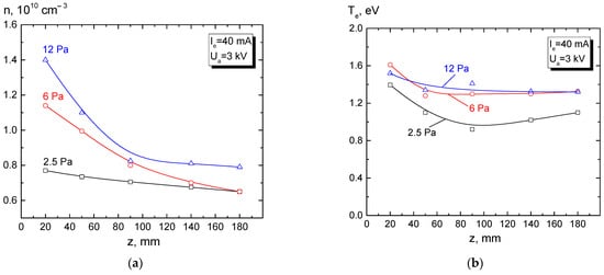
Figure 3. Longitudinal distributions of the concentration (a) and temperature (b) of the beam plasma generated during a free beam propagation in the chamber. Emission current Ie = 40 mA, beam energy Ua = 3 keV, argon [110].
The plasma concentration decreases along the beam propagation direction for both low (2.5 Pa) and higher pressure (12 Pa). Despite the concentration fall, the electron temperature (Figure 3b) weakly depends on the longitudinal coordinate. As noted in [111], a relatively weak change in the temperature may be caused by high thermal conductivity of electron gas. It is shown in [112] that the beam-plasma concentration increases with increasing beam current and its energy.
Paper [113] discusses the dependence of the electron temperature on the plasma concentration and on the beam energy recorded at a fixed position of a single Langmuir probe, Figure 4.
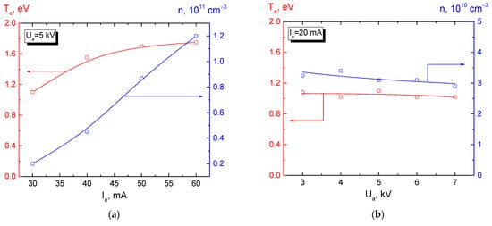
Figure 4. Dependence of parameters (n, Te) of the plasma generated in helium (5 Pa) during free beam propagation, on the beam current (a) and the beam energy (b). The probe is located 4 cm off the beam axis approximately half way on the beam transport path (z ≈ 92 mm) [113].
The results shown in this figure demonstrate a noticeable increase in the plasma concentration with an increase in the beam current. This can be related to the proportional dependence of the ionization on the beam current [114]. A smooth growth of the electron temperature with increasing beam current, as noted in article [108], may be related to a general increase in the fraction of the high-energy plasma electrons due to an increase in the concentration of beam electrons. It should be noted that the plasma concentration and electron temperature virtually do not depend on the beam energy (Figure 4b). The authors of [115] showed that with an increase in the pressure from 1 to 15 Pa, at a fixed current of about 30 mA and beam energy of up to 5 keV, the beam-plasma concentration increases, while the electron temperature decreases. Their calculations demonstrated that the cooling of plasma electrons, even disregarding inelastic collisions, mostly occurred through collisions with neutral molecules. The predominant mechanisms through which plasma electrons lose their energy are collisions with gas and the heat transfer from plasma by the electron flux. Thus, in the forevacuum pressure range of 1–15 Pa, using a focused electron beam, it is possible to create a plasma with a temperature of about 1 eV and a concentration of 109–1010 cm−3, the parameters of which can be controlled by several independent quantities: The beam current and energy, the pressure, and the type of gas.
Paper [116] reports the experimental studies of the spatial distribution of the concentration and temperature of electrons of the beam plasma created by a continuous ribbon electron beam with energy of up to 2 keV in an argon atmosphere at a pressure of 6 to 9 Pa. The electron beam, formed by the forevacuum plasma electron source, had a cross section of 10 mm × 250 mm. When propagating in the argon medium, the beam created a plasma which was confined in the electron-beam propagation region by creating a longitudinal magnetic field. It was demonstrated that the distributions of the electron concentration and temperature directly depend on the related distribution of the current density over the beam cross section, and the plasma parameters are essentially affected by the pressure in the vacuum chamber. Thus, with increasing pressure, the beam-plasma concentration increases to amounts up to 1010 cm−3 at a current density of 15 mA/cm2. A similar increase occurs with increasing beam current. The magnetic field strength affects the cross-section width of the “plasma sheet”. With increasing voltage, the plasma cross-section width decreases and simultaneously its concentration in the middle beam plane increases.
The parameters of the beam plasma, generated by a forevacuum plasma electron source of a ribbon electron beam with an energy of 2 keV and a beam size of 10 cm × 1 cm, transported without a magnetic field at a pressure of 5–10 Pa, are given in [117]. Unlike the case of plasma generation in the presence of a magnetic field [116], two beam-plasma interaction regimes are possible here. At relatively low beam currents (150–200 mA), the beam propagation in the transport region is characterized by a low concentration of the beam plasma (about 5 × 10¹⁵ m−3) and a low electron temperature (0.5 eV). A twofold increase in the beam current brings about a significant increase in the electron concentration and temperature, up to 1.5 × 10¹⁶ m−3 and 2 eV. The increase in the concentration is accompanied by an enhanced plasma glow [118]. Paper [119] presents the measurements of the parameters of the beam plasma generated during the propagation of a focused electron beam with an energy of up to 15 keV and a beam current of up to 300 mA in a helium atmosphere at a pressure of up to 50 Pa. The schematic diagram of the setup and the distribution of plasma concentration is shown in Figure 5.
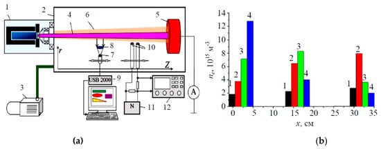
Figure 5. Experimental setup (a) and the beam-plasma parameters (b) [118,119]. Diagram: 1—plasma electron source, 2—vacuum chamber, 3—forevacuum pump, 4—electron beam, 5—collector, 6—beam plasma, 7—converging lens, 8—receiving part of the spectrometer, 9—optical spectrometer with a computer, 10—double Langmuir probe, 11—sawtooth voltage generator, 12—oscilloscope. Concentration distribution along the beam for an accelerating voltage of 14 kV and different positions of the beam crossover: 1—without crossover, 2—crossover near the collector, 3—crossover in the central part of the beam transport, 4—crossover near the electron source.
It has been demonstrated that the position of the region of intense interaction between the electron beam and plasma can be controlled by varying the beam current density, which is achieved by changing the position of the beam crossover. In the absence of a crossover, i.e., when the beam electrons move towards the collector along almost parallel trajectories, the concentration of plasma electrons varies weakly along the propagation path. By changing the beam focusing parameters and placing the crossover near the collector (at a distance of about 2 cm), or in the middle between the collector and the electron source, or near the electron source, one can observe in the corresponding area a maximum of the plasma electron concentration: The plasma concentration in this area increases by three times or more compared to the propagation of a uniform beam without a crossover (Figure 5). This article also demonstrates another effect related to the interaction of an electron beam and plasma: The formation of alternating bright and dark bands in the beam-plasma glow (Figure 6). The alternating bands were observed along the beam axis for a relatively narrow range of the beam parameters: at a beam current close to 200 mA, an accelerating voltage range of 8–14 kV and the beam crossover position of 5–7 cm from the collector (Figure 6b).
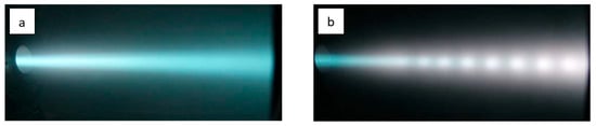
Figure 6. Photograph of a helium beam-plasma glow in the absence (a) and in the presence (b) of alternating bands. Beam current: a—180 mA, b—200 mA. Accelerating voltage 10 kV, pressure 40 Pa [119].
The observed phenomenon resembles strata, i.e., static or movable fringes of uneven luminosity alternating with dark bands in the positive column of a low-pressure gas discharge [120,121]. As noted by the authors in [119], the observed alternation of dark and bright bands, similar to strata, exists in a very narrow interval of the beam current and electron energy and may be related to the emergence of beam instability.
Injection of an electron beam into a dielectric cavity under high vacuum conditions is only possible if the negative charge brought by the beam is removed [122]. The use of forevacuum plasma electron sources allows one to bypass this physical limitation. The possibility of generating beam plasma entirely in a dielectric space has been demonstrated in [123], which reports the measurement of parameters of the beam plasma created during the injection of an electron beam into a cylindrical thin-walled quartz bulb with an inner diameter of 4 cm and a length of 20 cm (Figure 7). Experimental studies of the parameters of the generated beam plasma showed that the plasma potential inside the vessel was negative and increased with increasing pressure; and the beam-plasma concentration in the vessel was found to exceed the concentration of the plasma created by the beam in the free space of the vacuum chamber. In an earlier paper [124], it has been shown that there exist operational modes, in which the plasma occupies the entire space of the cavity even in the absence of any electrodes to remove the electric charge inside. In this case, the current is closed by a reverse flux of secondary electrons from the cavity surface, as well as through the beam plasma to the grounded parts of the vacuum chamber. It has been found in [124] that there exist generation regimes in which the plasma takes up the dielectric volume only partially (Figure 7a). With increasing pressure, the plasma fills the entire volume (Figure 7b). In addition, it has been shown for the first time that varying the gas pressure and the energy of the injected beam changes the character of the longitudinal distribution of the plasma concentration. With optimal parameters, the non-uniformity of concentration can be reduced to about 10% [118].
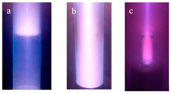
Figure 7. Plasma glow created in a dielectric cavity at a beam energy of 7 keV and a beam current of 20 mA, air pressure: (a)—1.5 Pa, (b)—4 Pa [124]. Beam-plasma sterilization: (c)—medical glass bottle of 10 mL.
The increased concentration has been explained based on the developed numerical model [125,126], which incorporates a numerical balance model that explains the increased concentration and the temperature of the beam-plasma electrons in the dielectric cavity by the additional energy contribution of secondary electrons knocked out by the beam electrons and plasma ions from the inner cavity surface and accelerated in the near-wall and near-bottom layers. It has been shown that the contribution of secondary electrons to ionization sharply increases in the gas’s lower range of pressure, whereas the contribution of plasma electrons remains negligibly small. Thus, the beam plasma in a confined space can be used for sterilization of medial glass and plastic bottles and vials (Figure 7c) [127].
2.3. Potential of a Dielectric Target Irradiated by an Electron Beam in Forevacuum
The beam plasma generated in the forevacuum pressure range, during the transport of the accelerated beam, can neutralize the electron-beam charging of electrically non-conductive surfaces (dielectrics). We modeled the plasma neutralization of the dielectric surface in the experiments on the electron-beam interaction with an insulated metal target [128]. The experimental setup is shown in Figure 8.
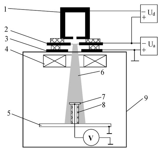
Figure 8. Experimental setup for irradiation of an insulated metal target by a cylindrical beam generated by a forevacuum plasma electron source: 1—hollow cathode, 2—anode, 3—accelerating electrode, 4—magnetic lens, 5—collector, 6—electron beam, 7—metal target, 8—insulator, 9—vacuum chamber [128].
The key question set in in the experiment was to determine the steady-state potential of the insulated metal target irradiated by electrons. Electron beam 6 was generated by a forevacuum plasma electron source, whose electrode scheme consisted of hollow cathode 1, flat anode 2, and accelerating electrode 3 [101]. Magnetic lens 4 was used to focus the electron beam. The focused electron beam hit the insulated stainless steel target 7. The target steady-state potential relative to the grounded collector and the vacuum chamber was measured using a high-resistance voltmeter.
In all experiments, the measured potential of the insulated metal target irradiated by the electron beam remained negative. As expected, the steady-state value of this potential increased with increasing electron-beam current and energy of accelerated electrons (Figure 9). At forevacuum pressures, the gas pressure is the predominant factor that diminishes the absolute value of the target potential [129].
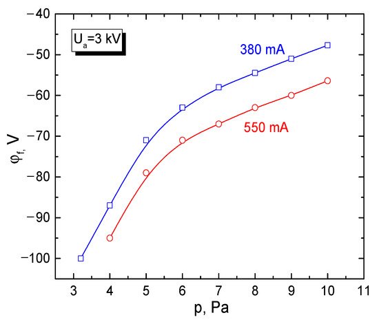
Figure 9. Dependence of the potential of insulated target on pressure. Working gas: helium. Electron-beam parameters: (Blue)—380 mA, 3 keV; (Red)—550 mA, 3 keV [129]. The potential is negative due to accumulation of negative charges on the surface.
As seen from the experimental dependences in Figure 9, already at a pressure of 10 Pa, under irradiation by an electron beam with an energy of 3 keV, the absolute value of the steady-state potential of the insulated target dropped down to 60–50 V. In the pulsed mode of operation of a forevacuum plasma electron source, at significantly higher electron-beam currents (for a microsecond pulse the electron-beam current amounts to tens of amperes), the absolute value of the potential is significantly higher and can reach 2500 V at an accelerating voltage of about 20 kV [130]. Note that according to experiments, at lower pressures, the electron beam charges the insulated metal target almost to the full magnitude of the accelerating voltage.
Thus, for the forevacuum pressure range, and all cases of the electron-beam action, the steady-state potential of the insulated metal target is either close to zero (low-current continuous electron beam) or much less than the accelerating voltage (high-current pulsed electron beam).
We have found from analysis of experimental data, theoretical estimates, and numerical modeling that in the forevacuum range, the steady-state potential of an insulated target is affected by the electron-beam parameters, and by the ion current to the target and secondary electron emission from the target surface [131]. An important additional factor that contributes to an increase in the ion flux to the insulated target is the discharge ignition between the negatively charged target and the vacuum chamber walls. In this case, the current of the discharge circuit closes via the electron beam. The discharge ignition manifests itself as an increase in the plasma glow in front of the insulated target, is accompanied by an increase in the plasma concentration in this area, and leads to a further decrease in the absolute value of the target potential [132].
When estimating the value of the steady potential of a dielectric target irradiated by an electron beam, one should account for a non-uniform distribution of the potential over the dielectric surface, as well as for the difference in the coefficients of secondary electron emission between metal and dielectric. Since the direct method of measuring the potential on a dielectric surface is virtually impossible, this potential was determined using indirect methods [133]. Thus, for measuring the potential on the alumina ceramic surface, a set of flat copper probes with a diameter of 3 mm was inserted into the dielectric target with a diameter of 30 cm [133]. The results for the target irradiated by an electron beam are shown in Figure 10. As follows from the data in Figure 10, the potential distribution over the surface of the dielectric target is non-uniform and, at the low-pressure value of forevacuum, the maximum value of the potential of a few kV is comparable to the accelerating voltage of 10 kV. However, a relatively slight increase in the pressure noticeably smoothens the potential distribution and significantly decreases the absolute value of its minimum.
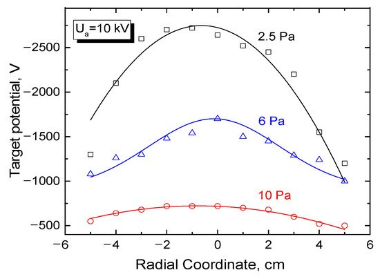
Figure 10. Distribution of floating potential of the set of probes installed in the dielectric target. Beam current 100 mA, electron energy 10 keV. Working gas is the residual atmosphere [133].
At a pressure as low as 10 Pa, the potential decreases to 700 V and almost compares with the case of the insulated metal target irradiated by an electron beam. As in the case of insulated metal target, an increase in the discharge current and in the accelerating voltage brings about the corresponding increase of the absolute value of the dielectric target surface potential. However, in this case, the potential stays well below the accelerating voltage that determines the electron energy.
Thus, the generation of dense beam plasma during the electron beam transport in forevacuum provides mostly complete neutralization by ions of the electron beam charging of the surface of an electrically non-conductive target. The charge compensation enables one to directly subject dielectric materials to the electron-beam processing, including the synthesis of dielectric coatings by electron-beam evaporation of dielectric targets.
2.4. Parameters and Characteristics of Dielectric Coatings
Electron-beam synthesis of dielectric coatings relies on using an electron beam for heating and evaporation of a dielectric target, followed by the deposition of evaporated products on the workpiece surface. As has been noted above, direct electron-beam evaporation of materials with low electrical conductivity can be implemented with the help of forevacuum plasma electron sources. In this case, the beam plasma generated by electron-beam evaporation can provide the ion-plasma assistance in coating deposition, while the use of chemically active gases as a working medium can affect the composition and structure of coatings and, therefore, their properties and parameters. The choice of optimal parameters of an electron beam is connected with thermal properties of the evaporated material of the dielectric target. The electron-beam optimal parameters, as well as thermal regimes of the electron-beam exposition, may greatly differ for different target materials. In this section, the electron-beam synthesis of dielectric coatings is presented using examples of the evaporation of alumina ceramics, boron, and silicon carbide.
2.4.1. Ceramic Coatings
Let us consider the process of heating, melting, and evaporation of a dielectric target using the example of aluminum oxide ceramics. An electron beam with a current of 150 mA and energy of up to 20 keV was focused on a diameter of 4 mm on a ceramic target (a cube with an edge of 1 cm). The evaporated ceramic sample, besides aluminum and oxygen, contained impurities of sodium, nitrogen, iron, silicon, and carbon (Figure 11). The ceramic cube was placed in a tantalum crucible. In the process of the electron-beam heating of the ceramic target, plasma was created nearby, which contained, together with the ions of the gas atmosphere, the ions of the evaporated material. The fraction of ions of the target material directly depends on the electron-beam power [134].
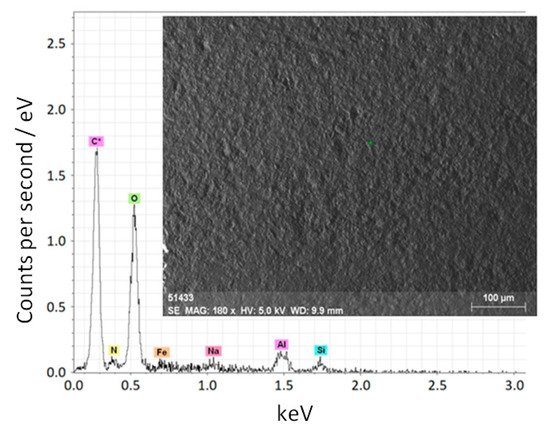
Figure 11. Elemental composition and micrograph of the initial aluminum oxide ceramics [134].
Using the experimental dependencies in Figure 12 of the ion composition on the electron-beam power density, one can see how the beam-plasma composition is changing during heating, melting, and evaporation of the ceramic target throughout the entire process of deposition (in this case, the entire cycle takes up to 1 min) [10]. At relatively low values of the beam power density (p = 2–4 kW/cm2) and accordingly of the electron-beam power during the ceramic sample heating, the sodium and potassium peaks in the mass spectra increase, together with the growth of the energy of the bombarding particles. The presence of these elements is due to their content in the raw materials, feldspars, used to manufacture ceramics, and because of their low molar heat of evaporation (Na—98 kJ/mol, K—77 kJ/mol) and a lower boiling point (Na—882.95 °C, K—773.85 °C) compared with aluminum (284.1 kJ/mol, 2518.85 °C). As a result, sodium and potassium are the first to evaporate from the surface layer of the ceramics into the vacuum chamber space. Relatively low values of ionization potentials of these elements (Na+—5.14 eV, K+—4.3 eV) provide effective ionization.
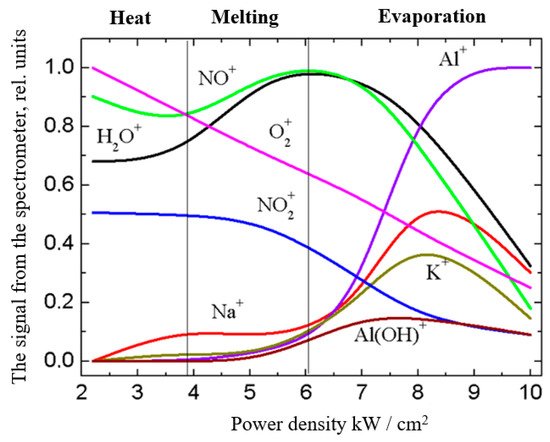
Figure 12. Mass-to-charge composition of the beam-plasma ions in the full cycle of coating deposition. Experimental parameters: Ie = 150 mA; Ua = 1–15 kV; p = 8 Pa [10].
With a further increase in the beam power density from 4 to 6 kW/cm2, the ceramic sample melts. In this range of power density, no noticeable change in the ion composition of the “ceramic” plasma is observed, and the amplitudes of sodium and potassium peaks remain at the same level. At a power density of above 6 kW/cm2, the sample temperature is high enough for evaporation and ionization of aluminum and its compounds. The peak amplitudes of sodium and potassium increase, which may be related to the evaporation of these elements from the bulk of the sample. At a power density of above 6 kW/cm2, the spectra show a sharp increase in the peaks of the elements contained in the ceramics. In this case, the peaks of the “ceramic” plasma ions begin to dominate over the “gas” plasma ions, which is indicative of the increased concentration of ceramic ions in the regions of registration of the beam-plasma ions and the substrate location. The peaks of the sodium and potassium curves at a beam power density of 8 kW/cm2 can be related to the evaporation of all additives used in the ceramic manufacture. At an electron-beam power density above 8.5 kW/cm2, the peaks of aluminum ions dominate the spectra [10].
Figure 13 shows micrographs of the ceramic coating and its elemental composition. As seen, the elemental composition of the coating deposited on the substrate almost matches the composition of the ceramic target (see Figure 11). The ratios of the components in the evaporated target and in the deposited coating differ.
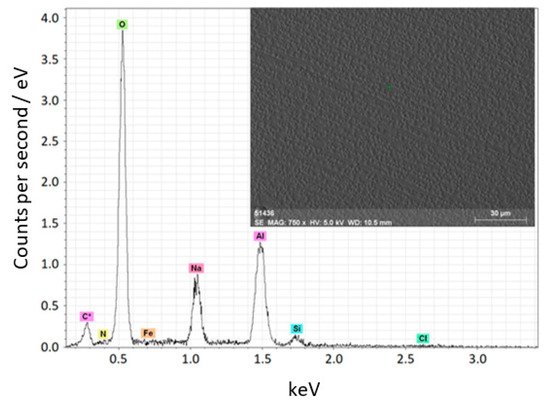
Figure 13. Elemental composition and micrographs of the coating deposited on a titanium substrate [134].
The experimental results in Figure 14 distinctly show two regions with a relatively slow and a faster increase in the rate of the target material evaporation with increasing electron-beam power. In the first case, the increase in the evaporation rate can be related to an increased temperature in the melt pool, as well as with the expansion of the pool’s area. In the second region, the sharp increase in the evaporation rate is connected with intense boiling of the material in the melt zone with the formation of the droplet fraction in the evaporated flux. Each of the ceramic target samples has a threshold power density at which a noticeable droplet fraction with a characteristic drop size of up to 20 µm appears. Depending on the composition of alumina ceramics and its thermal physical properties, the threshold power density for the appearance of the droplet fraction ranges from 1 to 10 kW/cm2. The presence of droplets in the evaporated flux degrades the quality of coatings. For this reason, the maximum electron-beam power density in the electron-beam synthesis of dielectric coatings must be restricted. It appears that the threshold value of the electron-beam power density for a particular evaporated material is a physical limitation imposed on the possibility of obtaining uniform ceramic coatings using the electron-beam evaporation in forevacuum. The target evaporation at a power density below the threshold enables one to form a uniform film on the substrate surface (Figure 15a).
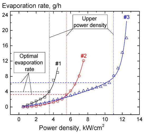
Figure 14. Evaporation rate during electron-beam evaporation of the target of a type of alumina ceramics vs. the electron-beam power density. Beam current up to 200 mA; pressure 10 Pa, beam diameter 5 mm.
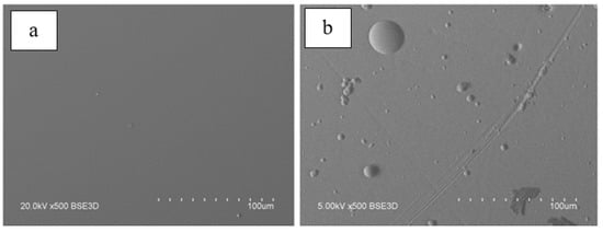
Figure 15. Surface micrographs of the coating based on alumina ceramics of different composition synthesized at different power densities: (a)—1 kW/cm2; (b)—10.5 kW/cm2.
At the maximum possible electron-beam power of 10 kW/cm2, the target evaporation rate is 5 g/h. With the electron-beam power density being the decisive factor that affects the evaporation rate, the coating thickness is normally controlled only by the process duration. In this case, it should be taken into account that for intensive evaporation, different ceramics must be heated up to different temperatures. Table 1 shows the coating thickness for evaporation of alumina ceramics of different compositions and corresponding deposition rates.
Table 1. Coating thickness and deposition rates.
| Sample 1 | Sample 2 | Sample 3 | Sample 4 |
|---|---|---|---|
| Coating Thickness, µm | |||
| 2.44 | 1.78 | 1.82 | 1.98 |
| Deposition Rate, nm/min | |||
| 1218 | 888 | 912 | 990 |
The obtained rate of the electron-beam deposition of ceramic coatings falls short of the characteristic values for electron-beam evaporation of metals. Nevertheless, it is much higher than that for the alternative method of magnetron sputtering of dielectric targets.
Figure 16 shows a photograph of a cross-section of a ceramic coating on a titanium substrate and the distribution of the elemental composition with the sample depth [135]. The high uniformity of the coatings and the absence of pores are connected with the high migration ability of the coating atoms at a high substrate temperature (over 700 °C) due to radiation heating. The high substrate temperature stimulates the formation of the crystal structure of coatings with the presence of Al2O3 γ- and α-phases. It should be noted that the elemental composition is constant with the depth, which is indicative of stability and uniformity of the deposition process.
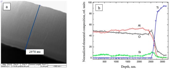
Figure 16. (a) A cross-section photograph of a ceramic coating on titanium. Experimental parameters: Ie = 150 mA; Ua = 1–15 kV; p = 8 Pa. (b) The elemental composition of the ceramic-based coating vs. the sample depth. Experimental parameters: p = 7.5 kW/cm2; p = 8 Pa [135].
The surface profile of this coating is shown in Figure 17. As seen, the roughness amplitude of the original sample is about 1 µm, and after the coating deposition, diminishes to 0.8 µm, which is over 20%. The width of non-uniformity peaks also decreases by over 60%, which indicates that the roughness of the sample surface reduces (Figure 17a) [135].
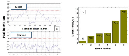
Figure 17. Surface profile of a ceramic-based coating on titanium: (a)—original and coated samples; (b)—micro-hardness of the original titanium sample and with the deposited Al2O3 coatings of different compositions [135].
The maximum micro-hardness amounts to 16 GPa, which almost matches the micro-hardness of aluminum oxide ceramics (Figure 17b). The coatings synthesized from the impurity-free ceramics possess the highest hardness. Such coatings have the most pure elemental composition, with only traces of oxygen and aluminum, and possess a granular surface structure. They also have higher Young’s modulus, though with an increased surface roughness.
Comparison of the electrical insulating parameters of the coating with those of the evaporated target material indicates their proximity (Table 2).
Table 2. Dielectric parameters of the original target and the deposited coating.
| Physical Parameter | VK-94-1 Ceramics | Coating |
|---|---|---|
| Dielectric constant at 20 °C and 10 kHz/10 MHz | 10.3/10.3 | 9/7.8 |
| Dielectric loss tangent tgδ·10−4 at 20 °C and 1 MHz | 6 | 5.9 |
| Volume resistivity, Ω·cm | 1013 | 1.2 × 10¹² |
One of the application examples of such dielectric coatings is their use of a heat sink from the integrated circuit surfaces [136].
2.4.2. Boron-Containing Coatings
Plasma with a high content of boron ions can be effectively generated and used for coating deposition by evaporation of a boron-containing target using a continuous focused electron beam of a forevacuum plasma source at a pressure of about 10 Pa. One of the specific features of boron at room temperature is its high electric resistivity (~106 Ω·cm). This resistivity drops sharply with increasing temperature. So, one should expect certain peculiarities of electron-beam evaporation of a boron sample regarding this feature, which should be taken into account when selecting the optimal evaporation regime for the synthesis of boron-based coatings.
A typical experimental setup for electron-beam evaporation of pure crystalline boron and boron nitride is shown in Figure 18 [137]. The electron source provided the generation of an electron beam with a current of up to 200 mA and energy of 1–20 keV. As a rule, the experimental cycle includes three stages. First, an electron beam of 100 mA and an accelerating voltage of up to 5 kV heats up the target to prevent it from cracking due to thermal stress. Then, the accelerating voltage slowly rises from 1 to 10 kV. When the critical electron-beam power is reached, the target begins to melt, and at a beam current of 200 mA and an accelerating voltage of 15–20 kV, the solid-body target evaporates, with the target temperature at this point being about 2500 °C.
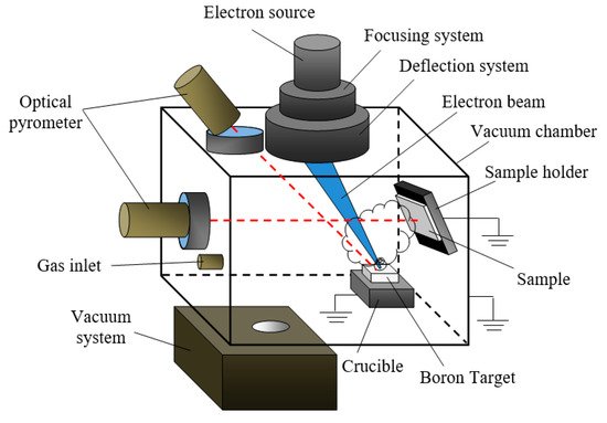
Figure 8. Experimental setup for depositing boron-containing coatings.
The temperature dependence of the boron target on the electron-beam power density is shown in Figure 19 [138].
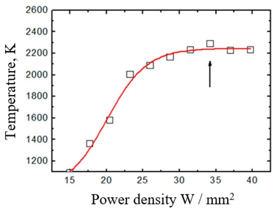
Figure 19. Temperature dependence of the boron target on the electron-beam power density: Ib = 80 mA; Db = 5 mm; p = 7 Pa [138]. Temperature saturates due to intensive evaporation after reaching the melting temperature (~ 2300 K).
The duration of the entire process was 5 to 20 min depending on the target composition (B or BN). Simultaneously with the deposition of coatings, it was possible to monitor the mass-to-charge composition of the beam plasma using a modified RGA-300 quadrupole mass-spectrometer [139,140]. Figure 20 shows photographs of the obtained boron-based coatings at different electron-beam power densities, and the distribution of micro-hardness with the depth of the coatings deposited during evaporation of boron and boron nitride in different gases. The data in the graphs allow one to indirectly determine the coating thickness. Since all graphs in the plots reach “saturation” at a pressure of ~1 GPa, which corresponds with the known tabular value of titanium Vickers micro-hardness (1 GPa), one can estimate the thickness of the coatings obtained from boron nitride in an atmosphere of different gases to be 3.5 µm. The thickness of the coating synthesized from boron in the residual atmosphere amounts to 5 µm.
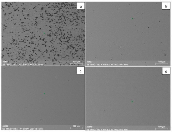
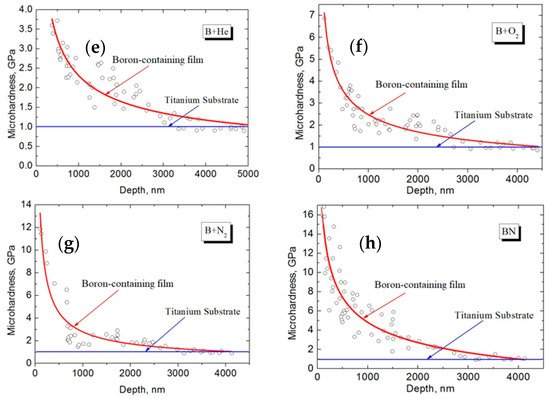
Figure 20. Photographs of boron-based coatings at different electron-beam power densities: (a) 30 kW/cm2; (b) 25 kW/cm2; (c) 20 kW/cm2; (d) 15 kW/cm2. Graphs [139] represent a micro-hardness of boron-containing coatings vs. depth during evaporation of boron in helium (e), oxygen (f), nitrogen (g), and of boron nitride in the residual atmosphere (h).
The conducted studies have shown that, despite approximately the same thickness, the boron-based coatings deposited in a gas medium, unlike boron nitride coatings, follow the substrate surface profile. There are visible long scratches left by the initial polishing of titanium substrates. As seen from the 3D surface profiles (Figure 21), the boron-based coatings deposited in different gas atmospheres contain many ridges and depressions. Their surfaces accommodate elements of a needle-like structure with a size of 0.1–0.5 µm, which can be caused by local chipping and destruction of thin surface layers due to internal stress.
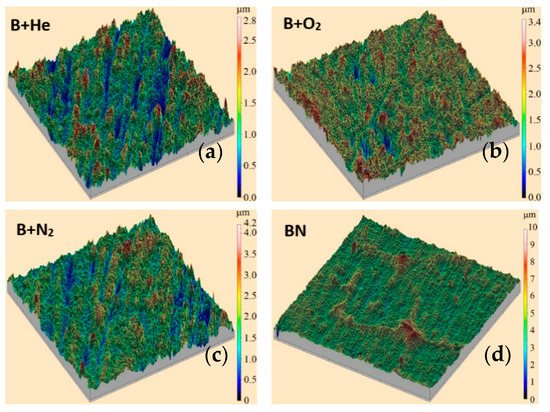
Figure 21. Three-dimensional profiles of the boron-based coatings synthesized during evaporation of boron in helium (a), oxygen (b), and nitrogen (c), and of boron nitride in the residual atmosphere (d) [139].
The presented profiles show that for the boron-based coating, the maximum profile height is 2.5 µm in the helium atmosphere, and about 3 µm in oxygen and nitrogen; while for boron nitride it is characterized by the presence of large inclusions with peaks of about 8 µm. The typical photographs and the elemental composition of the boron-containing and boron nitride coatings are shown in Figure 22. X-ray fluorescence analysis carried out on an XRD-7000S diffractometer (Shimadzu, Japan) showed (see Figure 22 a,c) that the boron-based coatings, fabricated by electron-beam evaporation of a pure boron target in an inert gas atmosphere, contain predominantly boron and oxygen. The spectra also contain lines of the substrate material (titanium).
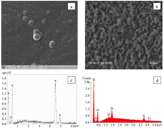
Figure 22. Surface photographs and the corresponding elemental composition of the boron-containing coating (a,c) and the boron nitride coating (b,d) [139].
The presence of oxygen is connected with its content in the residual atmosphere of the vacuum chamber and on the surface of the titanium substrate, which promoted its concentration both inside and outside of the fabricated films. The peaks of titanium and oxygen prevail over the boron lines, which is indicative of small thickness of the boron-containing layer. On the contrary, for boron nitride coatings (see Figure 22b,d), there is observed the highest peak corresponding to boron and weak lines of titanium and oxygen, which indicates a sufficiently thick boron-containing coating capable of absorbing the characteristic radiation of the substrate (titanium). The small amplitude of the oxygen line can be explained by the fact that the substrate is saturated with oxygen to a greater degree than the boron-containing coating or its surface layer. The presence of a large amount of impurities (magnesium, calcium, aluminum, and silicon) is due to the production method used to manufacture boron nitride targets, where magnesium is used as a production stimulator. The impurity lines have small amplitude, which indicates their insignificant content in the fabricated coating. The small amplitude of the nitrogen line is apparently associated with high absorption of characteristic nitrogen radiation by the formed coating, so that the spectrum contains only the lines of nitrogen atoms located predominantly in the near-surface layers [141].
Qualitative analysis of the coating showed that it contains atoms of boron, oxygen, carbon, and nitrogen (Figure 23). The presence of a considerable amount of boron (about 30–35%) throughout the entire coating thickness prompts the possibility of using forevacuum plasma electron sources for electron-beam evaporation of boron and deposition of a uniform boron coating.
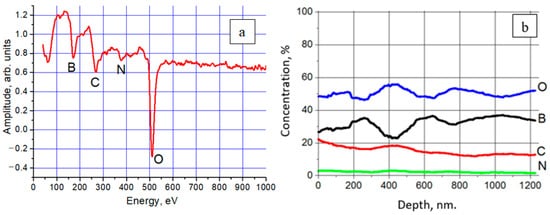
Figure 23. Elemental composition of the coating recorded using the Auger spectroscopy method from the sample surface (a) and its depth (b) [138].
It should be noted that the elemental composition of the coating is constant with the thickness, which confirms the stability and uniformity of the deposition process. The absence of the substrate elements in the coating at a depth of about 1 µm and a short deposition time (1 min) are indicative of a high deposition rate. The numerical values of the coating surface parameters are summarized in Table 3.
Table 3. Main surface parameters of coatings.
| Amplitude | Coating | |||
|---|---|---|---|---|
| B + He | B + O2 | +N2 | BN | |
| Root mean square roughness Sq, µm | 0.41 | 0.403 | 0.498 | 0.711 |
| Arithmetic roughness Sa, µm | 0.325 | 0.312 | 0.391 | 0.497 |
| Maximum surface relief height Sz, µm | 2.5 | 2.94 | 3.71 | 7.89 |
| The highest peak Sp, µm | 1.49 | 1.41 | 1.5 | 4.49 |
| The deepest depression Sv, µm | 1.08 | 1.7 | 3.93 | 3.69 |
| Asymmetry Ssk | 0.413 | –0.128 | 3.32 | 1.02 |
| Kurtosis Sku | 3.08 | 3.61 | 3.71 | 8.29 |
The parameter Sq, which is more sensitive to extreme values of roughness than Sa, made it possible to reveal the presence of individual sharp rough areas distinctly seen in the layout of the boron nitride coatings. Besides, there are artifacts in the form of larger peak-like violations of the surface uniformity. The profiles with a positive asymmetry coefficient are dominated by micro roughnesses with sharp high peaks that stand out from the average height. Negative values of Ssk characterize the surfaces with sharp deep depressions, such as the surfaces of the coatings obtained in the mixture of oxygen and nitrogen. This agrees with the graph in Figure 21. The combination of kurtosis and asymmetry can identify the surfaces which have relatively uniform high and low extreme points, such as, for example, the boron coatings in helium and nitrogen atmospheres.
2.4.3. Silicon-Carbon Coatings
Silicon-carbon coating (film) is a set of film structures that contains silicon and carbon atoms. These coatings are of interest to researchers and engineers due to a wide range of properties: chemical and thermal resistance, high Young’s moduli, low coefficient of thermal expansion, hardness, and high wear resistance. They usually have a low coefficient of friction, which is required for various moving mechanisms, and as such, silicon-carbon coatings are used as protective coatings in cutting tools, computer hard disks, and micro-electromechanical systems [142].
The experimental setup for the electron-beam synthesis of silicon-carbon coatings in principle does not differ from the experiments for production of ceramic or boron-based coatings. A high-temperature tantalum crucible, with a silicon carbide target inside, 0.5 cm thick and 1 cm in diameter, was placed at the bottom of the vacuum chamber. The SiC targets were prepared by uniaxial pressing at a pressure of 160–800 MPa at room temperature. Micrographs of the synthesized silicon-carbon coatings are shown in Figure 24. The rate of electron-beam evaporation of silicon carbide, and hence the deposition rate, increases with increasing electron-beam power density, so in order to avoid the formation of a droplet phase, the power density in experiments was restricted to a level of 7 kW/cm2. Morphology analysis of the surfaces of deposited coatings showed that the silicon-carbon film is a structure consisting of spherical grains ranging in size from hundreds of nanometers to a few micrometers. Similar results were previously obtained in [143], where the silicon-carbon coatings were produced using electrochemical deposition. Table 4 shows the data on micro-hardness and deposition time of silicon-carbon coatings in comparison with other deposition methods. As seen, the micro-hardness of the coatings obtained by electron-beam evaporation varies from 9 to 20 GPa and almost reaches the maximum for such coatings. Note that the synthesis by electron-beam evaporation of a 1000 nm coating takes only 10 min. As follows from the data in Table 3, this time is tens of times less as compared with alternative techniques. Note also the values of Young’s moduli (Figure 25).
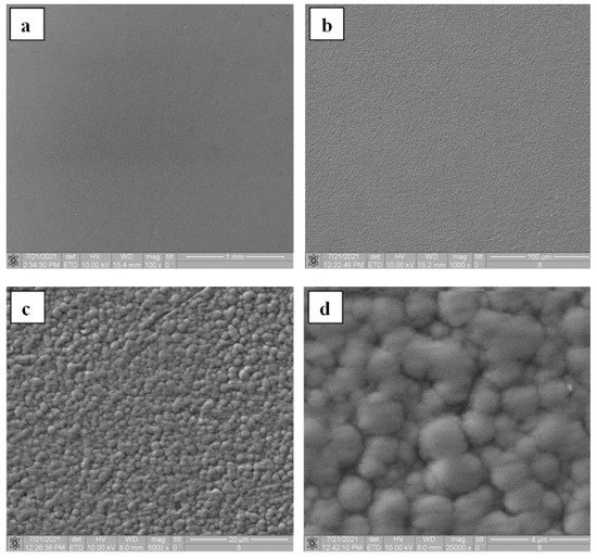
Figure 24. Micrographs of the obtained coatings at various magnifications: (a) 500×, (b) 1000×, (c) 5000×, (d) 25,000×.
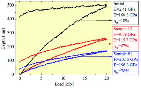
Figure 25. Test diagrams of the original and coated samples.
For the sample with a substrate temperature of 600 °C (Sample No. 1), Young’s modulus was about 200 GPa; for the sample with a substrate temperature of 300 °C (Sample No. 2), Young’s modulus was 115 GPa. Such a difference may be related to the elemental composition of the coatings (Figure 26). The coating of the sample with a higher temperature contains half as much oxygen and aluminum. These conclusions are in good agreement with the authors of [144].
Table 4. Comparison of micro-hardness and synthesis time of silicon-carbon coatings obtained by different methods.
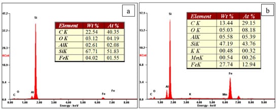
Figure 26. Elemental composition of obtained coatings: Sample No. 1 (a), Sample No. 2 (b).
Figure 25 shows the indenter loading curves for the original sample and for the samples with typical coatings. As seen from the figure, the obtained coatings have high values of elastic recovery, which may be indicative of an enhanced relaxation capacity of the material, especially stress relaxation under cyclic loads, which provides effective resistance to fatigue fracture [148].
Figure 26 shows the elemental composition of the obtained silicon-carbon coatings. The content of carbon ranges 30–40%, silicon 40–50%, oxygen 4–8%. It has been noticed that with an increase in the content of silicon, the hardness of coating decreases, which agrees well with the results of the authors of [144].
Figure 27 shows the results of tribological studies of the coated samples obtained at different substrate temperatures.
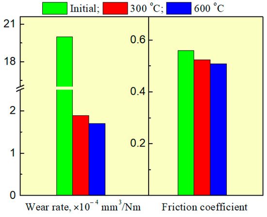
Figure 27. Results of tribological studies.
As seen, the synthesis of the silicon-carbon coating diminishes the coefficient of friction. The decrease in the coefficient of friction is greater with increasing substrate temperature. As a result, the surface wear resistance increases by over an order of magnitude. The use of forevacuum plasma electron sources for electron-beam evaporation of silicon carbide and the following deposition of vapor on the substrate make it possible to form silicon-carbide coatings with a thickness of several micrometers. The silicon-carbon coatings produced by this method have a coefficient of hardness of up to 20 GPa and Young’s modulus of about 200 GPa. The rate of the electron-beam deposition ensures that the required thickness of coating can be achieved in times that are tens of times shorter as compared with the known alternative techniques.
This entry is adapted from the peer-reviewed paper 10.3390/coatings12010082
This entry is offline, you can click here to edit this entry!