Silver (Ag), gold (Au), and copper (Cu) have been utilized as metals for fabricating metal-based inks/pastes for printed/flexible electronics. Among them, Cu is the most promising candidate for metal-based inks/pastes. Cu has high intrinsic electrical/thermal conductivity, which is more cost-effective and abundant, as compared to Ag. Moreover, the migration tendency of Cu is less than that of Ag. Thus, recently, Cu-based inks/pastes have gained increasing attention as conductive inks/pastes for printed/flexible electronics. We can divide Cu-based inks/pastes into four categories from the viewpoints of Cu sources: (i) traditional micron-sized flake/powder type, (ii) nanoparticle type, (iii) nanowire type, and (iv) precursor ion type. However, the disadvantages of Cu-based inks/pastes are their instability against oxidation under an ambient condition and tendency to form insulating layers of Cu oxide, such as cuprous oxide (Cu2O) and cupric oxide (CuO). The formation of the Cu oxidation causes a low conductivity in sintered Cu films and interferes with the sintering of Cu particles. The surface and interface designs for Cu-based conductive inks/pastes are important strategies for the oxidation resistance of Cu and low-temperature sintering to produce highly conductive Cu patterns/electrodes on flexible substrates. The surface control approaches include surface designs by polymers, small ligands, core-shell structures, and surface activation. The Cu-based mixed inks/pastes offer improved performances compared with the single use of each component.
- copper
- nanoparticles
- complexes
- inks
- pastes
- printed electronics
- flexible devices
Copper (Cu)
Copper (Cu) is one of the significant metals in the industry that can be used in various applications. It has several excellent properties, including electrical conductivity, thermal conductivity, and antimicrobial activity [1]. An alloy can be fabricated using Cu in combination with other elements, such as gold (Au), silver (Ag), aluminum (Al), nickel (Ni), tin (Sn), and zinc (Zn), to improve its properties, such as corrosion resistance or machinability. Besides, the ease of fabrication and the cost-effectivity of Cu are also important in industrial applications. The high electrical conductivity (i.e., low resistivity, ~1.68 Wcm) is the most attractive characteristic of Cu as an electronic material [1]. For the last 10 years, novel electronic forms have been developed from their traditional rigid/bulky forms to soft/thin forms which are flexible, bendable, and stretchable. The softness is attributed to the use of flexible substrates, such as polymers (polyethylene terephthalate (PET), polyethylene naphthalate (PEN), polyimide (PI), and polycarbonate (PC)), paper, textiles, and rubber. Recent printing technologies, including flexography, offset, gravure, screen printing, and inkjet printing, offer the direct deposition of conductive materials on flexible substrates for the cost-effective/large-scale fabrication of flexible electronics [2].
Conductive Inks/Pastes for Printed/Flexible Electronics
Printed electronics are essential to facilitate the widespread use of flexible electronics and, more recently, stretchable electronics, such as sensors, electronic displays, solar cells, thin-film transistors, and supercapacitors [3–14]. Printable conductive electrodes on flexible substrates require the following characteristics for the application of printed electronics: (i) a high conductivity, (ii) cost-effectiveness, (iii) durability under extreme environmental conditions (heat and moisture), and (iv) printing processability on low-cost plastic substrates (indispensably, PET for productive roll to roll (R2R) processes). In the printing process, conductive materials dispersed in solvents (i.e., ink/paste) are deposited on flexible substrates in pre-designed patterns. Numerous types of conductive inks/pastes have been developed by using various conductive sources, such as graphene, carbon (C) nanotubes, metal (Ag, Au, and Cu) nanoparticles/nanowires, metal oxide (Zn, Al, and Sn) nanoparticles, conducting polymers, and organic-metal complexes, for different applications [15–17]. These conductive materials have advantages and disadvantages for conductive inks/pastes. Conductive organic inks/pastes (i.e., polymers and carbon) are suitable for flexible electronics owing to their natural softness. Moreover, they are well compatible with polymer substrates. However, their electrical conductivities are not ideal for electronic applications. Metal-based inks/pastes have advantages in terms of their high electrical/thermal conductivities. However, their flexibility and extensibility are insufficient to fabricate flexible and stretchable devices. Besides, the binding of metals to polymer substrates is weak without the use of an adhesive. Solving such problems remains challenging for conductive inks/pastes in printed/flexible electronics.
Copper-Based Conductive Inks/Pastes
Ag has been utilized as a metal for fabricating metal-based inks/pastes for printed/flexible electronics. Ag has a high electrical conductivity among various metals, and it is relatively cost-effective compared with Au. The oxidation of Ag occurs slowly, slightly affecting the conductivity of Ag-based inks/pastes over time. Besides, Ag nanoparticle-based inks can produce conductive films at low-temperature sintering (less than 150 °C), and this is the advantage of the formation of conductive patterns on flexible substrates with a low heat resistance. For these reasons, Ag-based inks/pastes have been frequently used as metal-based inks/pastes and commercialized by numerous companies. The current challenge is the replacement of Ag by other cheaper conductive metals, such as Cu, Al, or Ni. Among these metals, Cu is the most promising candidate for metal-based inks/pastes. Cu has a high intrinsic electrical/thermal conductivity (similar to Ag and higher than Au), and it is more cost-effective and abundant (about 1% of the price of Ag and 1000 times abundant than Ag). More importantly, the migration tendency of Cu is less than that of Ag. Recently, therefore, the Cu-based inks/pastes for printed/flexible electronics have gained increasing attention. However, the disadvantages of Cu-based inks/pastes include their instability against oxidation under an ambient condition and their tendency to form insulating layers of Cu oxide, such as cuprous oxide (Cu2O) and cupric oxide (CuO). The formation of the oxidation layer causes a low conductivity of sintered films and interference in the sintering process of Cu particles.
In the past decade, thus, numerous researchers have developed stable Cu-based inks/pastes[18-21]. Herein, we adopt the viewpoints of the surface and interface designs for Cu-based inks/pastes, as summarized in Figure 1. The surface control approaches include surface designs by polymers (polyvinyl pyrrolidone (PVP), gelatin, polyethylene glycol (PEG), small ligands (oleylamine, alkanolamine, lactic acid, ascorbic acid, citric acid, oleic acid, and alkanethiols), core-shell structures (metal shell/alloy, carbon, Cu oxide), and surface activation. The Cu-based mixed inks/pastes offer improved performances compared with the single use of each component, such as Cu nano/microparticles, metal-organic decomposition (MOD)/Cu particles, Cu nanowires/Cu nano or MOD inks, and carbon nanotube/Cu-based Inks.
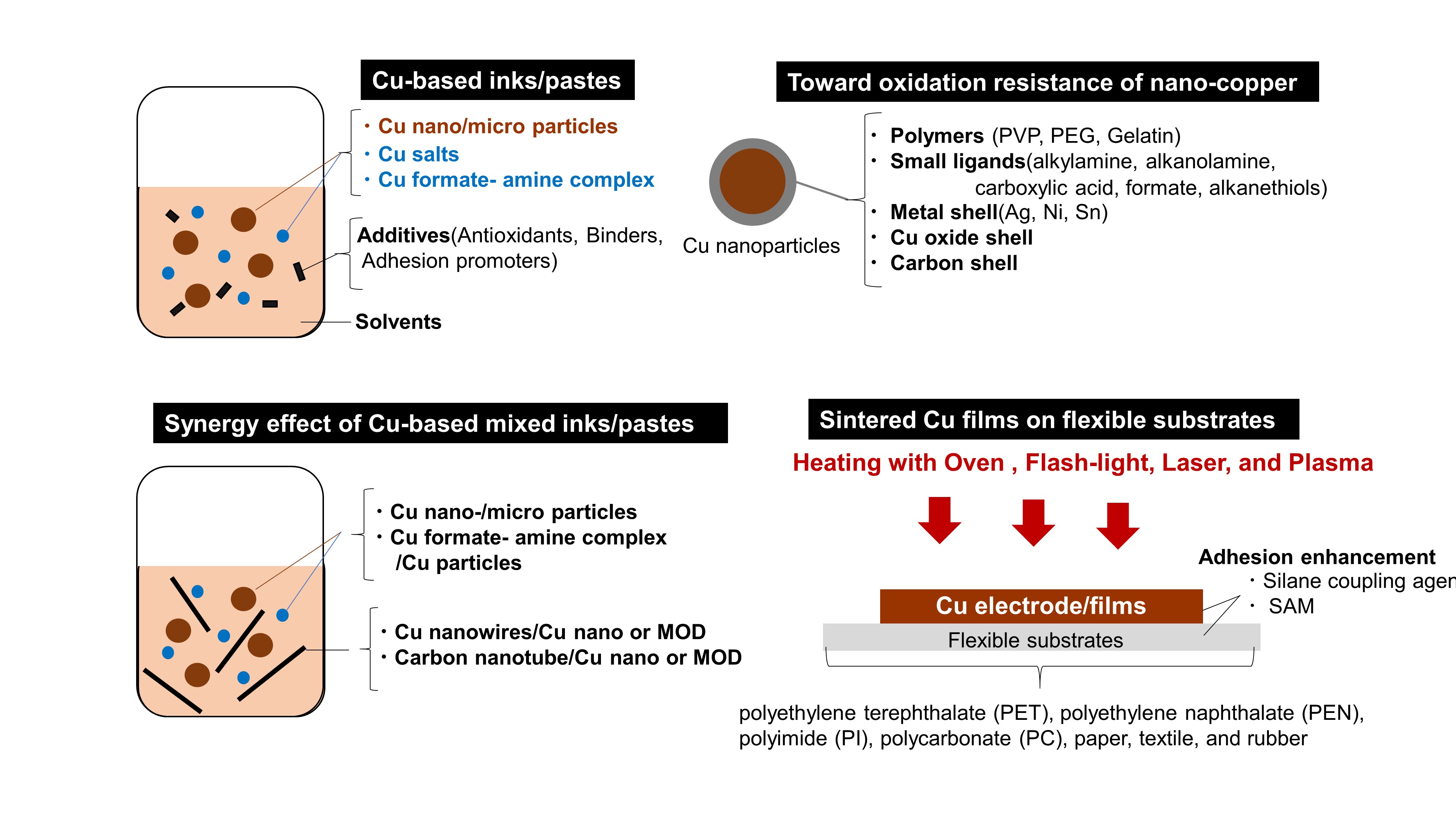
Figure 1. Strategies for Cu oxidation resistance and low-temperature sintering by the surface and interface designs in Cu-based conductive inks/pastes.
Main components of Cu-Based Inks/Pastes
The main components of Cu-based inks/pastes are as follows:(i)Cu particles or their precursors (e.g., Cu salts or Cu formate-amine complex) as conductive fillers. (ii) Solvents for the stable dispersion of Cu particles or dissolution of their precursors, facilitation of transport/drying of the ink/pastes, and control of viscosity/surface tension for printing. Besides, reductive solvents, such as ethylene glycol (EG), can be used for Cu-based inks/pastes to suppress Cu oxidation at high temperatures. (iii) Dispersion and protective agents for the dispersion stability of Cu particles and the Cu oxidation resistance. (iv)Other additives to enhance or modify the properties of the ink/paste (e.g., antioxidants, binders, and adhesion promoters).
Categories of Cu-Based Inks/Pastes
We can divide Cu-based inks/pastes into four categories from the viewpoints of Cu sources (Figure 2): (i) traditional micron-sized flake/powder type, (ii) nanoparticle type, (iii) nanowire type, and (iv) precursor ion type. The sintering temperature ranges from 50 to 80% of the melting temperature of the material, but for nanosized powders, the sintering temperature can be much lower, i.e., 20 to 30% of the melting temperature [22]. Thus, the application of micron-sized powder-based pastes is limited to low-temperature sintering. Compared with micron-sized Cu powders, nanoparticle-based inks have a much lower sintering temperature (<250 °C). When the particle size of a metal reaches the nanoscale, its melting point decreases [23], thus resulting in the reduction in the sintering temperature of the Cu nanoparticles. The reduction in the total interfacial energy causes this sintering process of Cu nanoparticles via the densification–reduction in the solid/liquid interfacial area. Using Cu nanoparticle-based inks, we can obtain sintered Cu films at low-temperature (<150 °C) sintering on the thermal-sensitive flexible substrates (e.g., polymer, paper, textile, and rubber). The Cu precursor ink (category iv) is also useful for reducing the process temperature. Cu precursors are metals in oxidized forms, which can be organic Cu complexes, such as Cu formate complexes with various alkylamines. During the thermal process, the Cu precursor is decomposed and causes the in-site formation of Cu nanoparticles at temperatures less than <150 °C, resulting in the conductive Cu film on flexible substrates. Flexible electrical devices should maintain their electrical performances under some mechanical deformations, such as bending, twisting, and stretching. However, sintered metallic NPs films tend the strain fracture by these mechanical deformations. Besides, sintered Cu films often involve porosity and micro-cracks within the film. Such defects could accelerate the initiation and growth of cracks, which could result in a lower mechanical strength of the film. Cu nanowires (Cu NWs) can improve the microstructure, conductivity, and mechanical stability of the sintered Cu films owing to their high mechanical strength and electrical conductivity
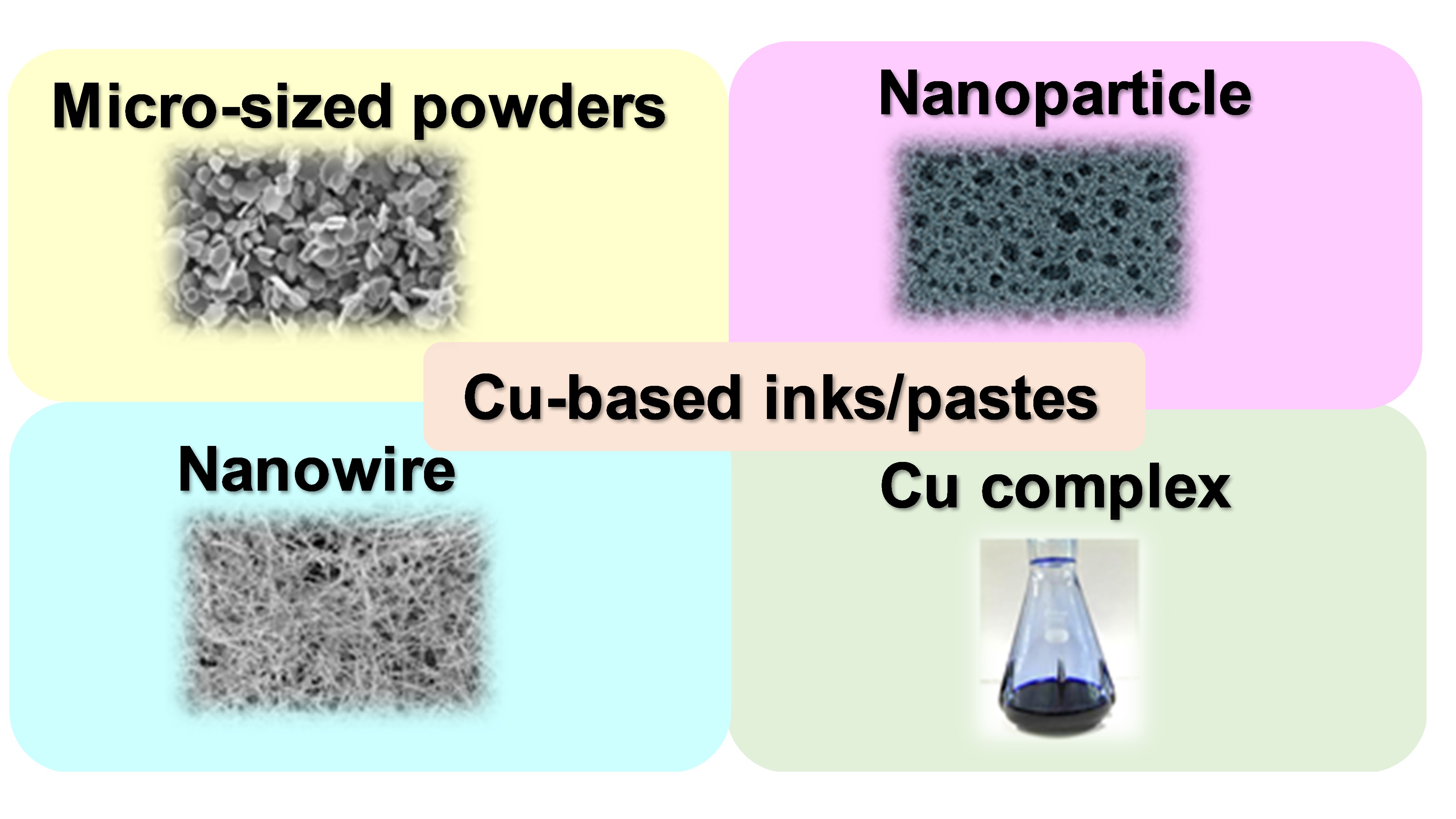
Figure 2. Categories of Cu-based inks/pastes.
Applications
The Cu-based inks/pastes would allow a real application of flexible devices such as smart robotics, electronic skin, optoelectronics, human motion, health monitoring systems, and human–machine interactive systems. Human-friendly stretchable electronics, combined with analytical biosensing, are extending the concept of healthcare and enabling much more accurate and comfortable monitoring in real-time. High-power semiconductor devices, such as SiC and GaN, with wideband gaps, are expected to function for an extended period at temperatures above 200 °C, even 350 °C, which is too high for the traditional die-attach materials that are currently used widely. Cu-based inks/pastes have high potentials for low-temperature Cu–Cu bonding for high-power semiconductor devices as the next-generation die-attach nanomaterials.
References
- Davis, J.R. Asm Specialty Handbook: Copper and Copper Alloys; ASM international: Novelty, OH, USA, 2001.
- Khan, Y.; Thielens, A.; Muin, S.; Ting, J.; Baumbauer, C.; Arias, A.C. A New Frontier of Printed Electronics: Flexible Hybrid Electronics. Mater. 2020, 32, 1–29, doi:10.1002/adma.201905279.
- Sreenilayam, S.P.; Ahad, I.U.; Nicolosi, V.; Acinas Garzon, V.; Brabazon, D. Advanced Materials of Printed Wearables for Physiological Parameter Monitoring. Today 2020, 32, 147–177, doi:10.1016/j.mattod.2019.08.005.
- Yu, Y.; Nyein, H.Y.Y.; Gao, W.; Javey, A. Flexible Electrochemical Bioelectronics: The Rise of In Situ Bioanalysis. Mater. 2020, 32, 1–25, doi:10.1002/adma.201902083.
- Ma, Y.; Zhang, Y.; Cai, S.; Han, Z.; Liu, X.; Wang, F.; Cao, Y.; Wang, Z.; Li, H.; Chen, Y.; et al. Flexible Hybrid Electronics for Digital Healthcare. Mater. 2020, 32, 1–23, doi:10.1002/adma.201902062.
- Kim, D.C.; Shim, H.J.; Lee, W.; Koo, J.H.; Kim, D.H. Material-Based Approaches for the Fabrication of Stretchable Electronics. Mater. 2020, 32, 1–29, doi:10.1002/adma.201902743.
- Gerislioglu, B.; Dong, L.; Ahmadivand, A.; Hu, H.; Nordlander, P.; Halas, N.J. Monolithic Metal Dimer-on-Film Structure: New Plasmonic Properties Introduced by the Underlying Meta. Nano Lett. 2020, 20, 3, 2087–2093, doi:10.1021/acs.nanolett.0c00075.
- Gerislioglu, B.; Bakan, G.; Ahuja, R.; Adam, J.; Mishra, Y.K.; Ahmadivand, A. The Role of Ge2Sb2Te5 in Enhancing the Performance of Functional Plasmonic Devices. Today Phys. 2020, 12, 2542–5293, doi:10.1016/j.mtphys.2020.100178.
- Xue, Z.; Song, H.; Rogers, J.A.; Zhang, Y.; Huang, Y. Mechanically-Guided Structural Designs in Stretchable Inorganic Electronics. Mater. 2020, 32, 1–32, doi:10.1002/adma.201902254.
- Yao, S.; Ren, P.; Song, R.; Liu, Y.; Huang, Q.; Dong, J.; O’Connor, B.T.; Zhu, Y. Nanomaterial-Enabled Flexible and Stretchable Sensing Systems: Processing, Integration, and Applications. Mater. 2020, 32, 1–31, doi:10.1002/adma.201902343.
- Kim, K.; Kim, B.; Lee, C.H. Printing Flexible and Hybrid Electronics for Human Skin and Eye-Interfaced Health Monitoring Systems. Mater. 2020, 32, 1–22, doi:10.1002/adma.201902051.
- Xiang, L.; Zeng, X.; Xia, F.; Jin, W.; Liu, Y.; Hu, Y. Recent Advances in Flexible and Stretchable Sensing Systems: From the Perspective of System Integration. ACS Nano 2020, 14, 6449–6469, doi:10.1021/acsnano.0c01164.
- Sajedi-Moghaddam, A.; Rahmanian, E.; Naseri, N. Inkjet-Printing Technology for Supercapacitor Application: Current State and Perspectives. ACS Appl. Mater. Interfaces 2020, 12, 34487−34504, doi:10.1021/acsami.0c07689.
- Li, H.; Liang, J. Recent Development of Printed Micro-Supercapacitors: Printable Materials, Printing Technologies, and Perspectives. Mater. 2020, 32, 1–19, doi:10.1002/adma.201805864.
- Naghdi, S.; Rhee, K.Y.; Hui, D.; Park, S.J. A Review of Conductive Metal Nanomaterials as Conductive, Transparent, and Flexible Coatings, Thin Films, and Conductive Fillers: Different Deposition Methods and Applications. Coatings 2018, 8, 278, doi:10.3390/coatings8080278.
- Nayak, L.; Mohanty, S.; Nayak, S.K.; Ramadoss, A. A Review on Inkjet Printing of Nanoparticle Inks for Flexible Electronics. Mater. Chem. C 2019, 7, 8771–8795, doi:10.1039/c9tc01630a.
- Joo, H.; Jung, D.; Sunwoo, S.H.; Koo, J.H.; Kim, D.H. Material Design and Fabrication Strategies for Stretchable Metallic Nanocomposites. Small 2020, 16, 1–19, doi:10.1002/smll.201906270.
- Abhinav, K., V.; Rao, R., V.K.; Karthik, P.S.; Singh, S.P. Copper Conductive Inks: Synthesis and Utilization in Flexible Electronics. RSC Adv. 2015, 5, 63985–64030, doi:10.1039/c5ra08205f.
- Cano-Raya, C.; Denchev, Z.Z.; Cruz, S.F.; Viana, J.C. Chemistry of Solid Metal-Based Inks and Pastes for Printed Electronics–A Review. Mater. Today 2019, 15, 416–430, doi:10.1016/j.apmt.2019.02.012.
- Feng, Y.; Zhu, J. Copper Nanomaterials and Assemblies for Soft Electronics. China Mater. 2019, 62, 1679–1708, doi:10.1007/s40843-019-9468-5.
- Li, W.; Sun, Q.; Li, L.; Jiu, J.; Liu, X.Y.; Kanehara, M.; Minari, T.; Suganuma, K. The Rise of Conductive Copper Inks: Challenges and Perspectives. Mater. Today 2020, 18, 100451, doi:10.1016/j.apmt.2019.100451.
- Groza,J.R. Nanosintering. Nanostructured Materials 1999, 12, 987–992, doi:10.1016/S0965-9773(99)00284-6.
- Allen, G. L.; Bayles, R. A.; Gile, W. W.; Jesser, W.A. Small particle melting of pure metals. Thin Solid Films 1989, 144, 197-308, doi.org/10.1016/0040-6090(86)90422-0.
This entry is adapted from the peer-reviewed paper 10.3390/nano10091689