Interpenetrating bulk heterojunction (IBHJ) quantum dot solar cells (QDSCs) offer a direct pathway for electrical contacts to overcome the trade-off between light absorption and carrier extraction. However, their complex three-dimensional structure creates higher requirements for the optimization of their design due to their more difficult interface defect states control, more complex light capture mechanism, and more advanced QD deposition technology. ZnO nanowire (NW) has been widely used as the electron transport layer (ETL) for this structure. Hence, the optimization of the ZnO NW morphology (such as density, length, and surface defects) is the key to improving the photoelectric performance of these SCs.
1. Introduction
The world environmental and energy crisis calls for the imminent development of renewable or nonconventional energies. As the most abundant source of clean energy on the planet, solar energy is an important approach to achieving the goal of carbon neutrality in the future [
1]. To date, three generations of solar cells have been evolved to harvest solar energy as efficiently as possible [
2], but they are still fundamentally limited in terms of solar cell efficiency, including thermalization losses from the absorption of high-energy photons, the non-absorption of low-energy photons, extraction losses due to unavoidable charge carrier recombination, and other mechanisms of energy loss [
3].
Quantum dot solar cells offer the advantage of a zero-dimensional structure [
4]. Due to their remarkable multiple exciton generation [
5,
6], hot carrier effect [
7], possible intermediate band cell structure [
8,
9,
10], and multi-junction cell structure [
11,
12], QDSCs offer the real possibility of boosting energy conversion efficiency beyond the Schockley and Queisser (SQ) limit of 32% for traditional silicon-based SCs [
13]. In the past few decades, QDs have been widely researched and integrated in various kinds of SCs, such as Schottky junction colloidal quantum dot (CQD) SCs [
14,
15], depleted heterojunction CQDSCs [
16,
17,
18], quantum junction CQDSCs [
19,
20,
21], and quantum dot-sensitized solar cells (QDSSCs) [
22,
23,
24]. However, the PbS QDSCs that have been widely studied have only reached a record efficiency of 13.3% [
25], which is far from the theoretical efficiency of 45% for a single-junction solar cell [
26]. The main reason for this situation is that various sub-band gap trap states could be introduced in the synthesis and ligand exchange processes of CQD materials. CQDSCs are still limited by the trade-off between carrier extraction and light absorption. A typical planar n-p-p
+-type PbS QDSC usually features an absorption layer that is only about 300 nm thick, while a thickness of QD film of about 1 μm is required to achieve the full absorption of solar radiation. Generally, limited carrier diffusion length (L
D) and depletion width (W
D) are the main factors limiting the thickness of the absorption layer [
27]. Thus, maximizing the recombination lifetimes of both charge carriers and their transport properties, which are related to L
D and W
D, is essential to achieve further advances in the thickness of the absorption layer. The IBHJ structure is considered to be another effective solution. IBHJ QDSCs feature a driving force to separate and transport the carriers with band bending and, at the same time, orthogonalize the direction of light absorption and electron–hole pair (EHP) separation, so that the absorber layer is thick enough to produce photocarriers that can be utilized [
18]. Their n-type metal oxide acceptor is composed of 1D NWs (usually TiO
2 or ZnO; here, we mainly focus on ZnO, since it easily synthesizes various nanostructures and offers higher electron mobility than TiO
2). Simulation studies have shown that compared with planar solar cells, this type of cell structure is particularly advantageous when the optical absorption depth is comparable to the thickness of the device and the rate of carrier recombination in the depletion region is relatively large [
28,
29]. In addition, 3D structures have been shown to reduce surface optical reflection and enhance the absorption efficiency of SCs [
30,
31]. Moreover, the bending durability of ZnO NW arrays may offer promising prospects to meet the demands of flexible photovoltaic devices. Under bending conditions, interpenetrating structures can effectively release stress and thus resist the performance degradation caused by bending better than comparable planar devices [
32]. Recently, a record short-circuit current density (JSC) of 33.2 mA cm
−2 with a power conversion efficiency (PCE) of 10.62% was demonstrated for a PbS IBHJ QDSC employing the luminescence down-shifting method [
33]. Further improvements of device performance require fine control of the morphology of NWs. For instance, in a piezoelectric strain sensor, inclined nanowires respond well to vertical contact forces, while vertically aligned nanowires are more sensitive to surface flow [
34]. In IBHJ QDSCs, a better vertical arrangement of NWs can prevent the formation of large voids during the deposition of QDs [
35]; the density, length, and surface defects of NWs directly affect the final performance of SCs. Besides, in real-world applications, different synthesis methods often feature different levels of morphology control precision, and the synthesis method must be considered to adapt to the application system of QDSC mass production. Therefore, it is necessary to review the preparation process of NW and analyze the morphology optimization mechanism of NWs.
2. Optimization Strategies of IBHJ QDSCs Based on ZnO NWs
2.1. Geometrical Morphology Optimization of Nanowires
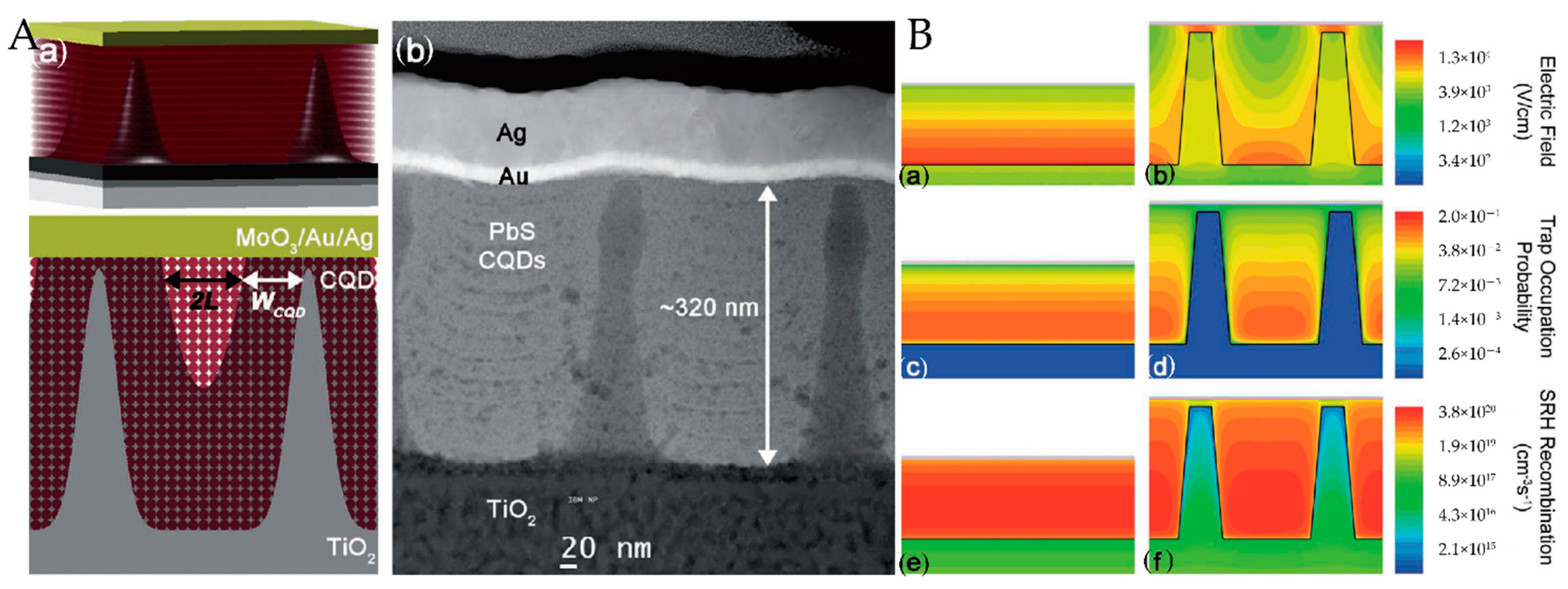
The original intention to develop this bulk heterojunction structure was to increase the electrical contact area between the donor and the acceptor so that the photocarriers can be collected before they are captured by trap states. Moreover, NWs allow the light absorption and carrier extraction to be controlled independently [
83]. Therefore, our core aim can be summarized as obtaining efficient carrier extraction and the increased thickness of light-absorbing materials. As early as 2012, Kramer et al. [
96] proposed the spacing of nanopillars in their research on TiO
2 NWs QDSCs (
Figure 7). However, longitudinal carrier collection is neglected, and this process often affects the overall thickness of the SCs.
Figure 7. (
A) (
a) Schematic and (
b) SEM images of CQDSCs; (
B) electric field distributions, trap occupation, and SRH recombination of planar and nanopillar architectures [
96].
Considering the efficient collection of photocarriers, it is necessary to distinguish between the electron and hole collection processes. To collect photogenerated electrons efficiently, the pitch size of the NWs should meet the following requirements (Figure 8),
where dnp–np is the average spacing of NWs and dtop is the distance from the top of the NW to the back electrode. Notably, dtop is an upper bound on collection length. The depletion situation at the top of the nanowires is usually more complicated. Electrons are mainly collected horizontally, whereas holes often need to be transported vertically to the host electrode to form photocurrents. Therefore, the limited collection length of holes directly limits the length of the NWs and, thus, the thickness of the light-absorbing layer material,
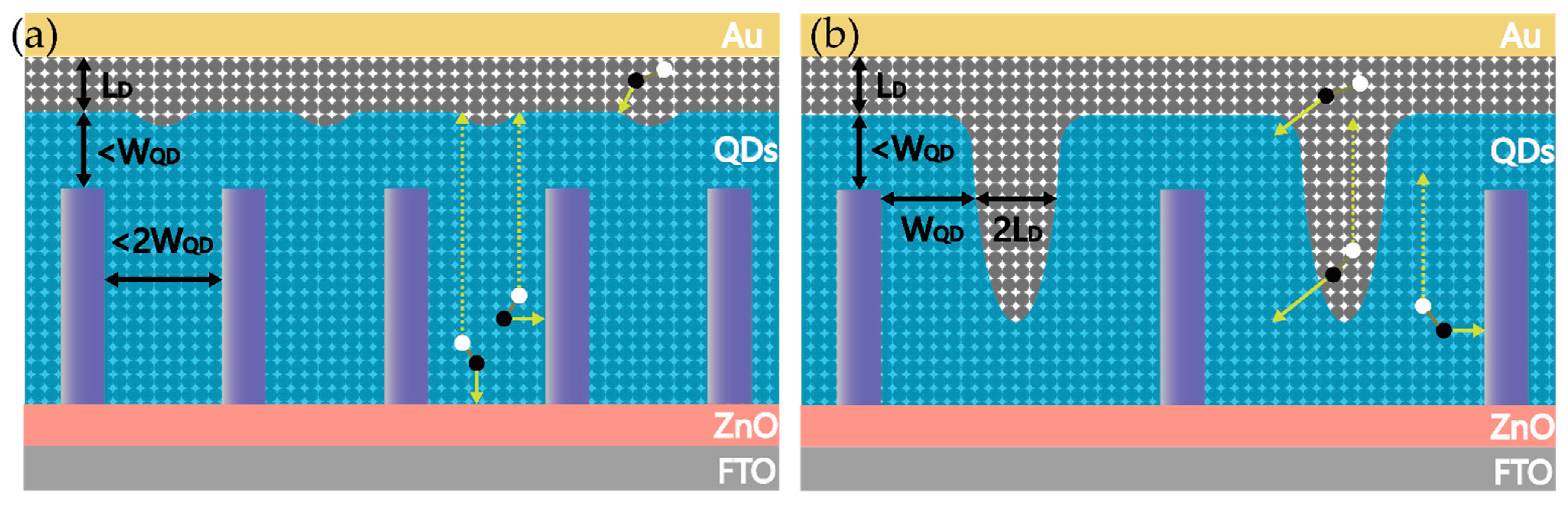
Figure 8. (a) IBHJ structure based on hydrothermal method; (b) ideal IBHJ structure.
Table 3. Characteristic parameters of several lead chalcogenide QD material layers.
| Ligand |
CQD Material |
CQDSC Structure |
Doping Density (cm−3) |
Depletion Width (nm) |
Diffusion Lengths (nm) |
PCE (%) |
| Organic ligand |
PbS-MPA
[95] |
- |
- |
- |
30 |
- |
PbS-MPA
[97] |
- |
- |
- |
70 |
- |
| Halide ligand |
PbS-PbX2
[98] |
ITO/ZnO/PbS-PbX2/PbS-EDT/Au |
9.94 × 10¹⁶ |
165 |
52 |
7.2 |
PbO-PbS-TBAI
[99] |
ITO/ZnO/PbS-TBAI/PbS-EDT/Au |
- |
- |
61 |
9.4 |
PbAc-PbS-TBAI
[99] |
ITO/ZnO/PbS-TBAI/PbS-EDT/Au |
- |
- |
95 |
10.8 |
PbS-TBAI
[95] |
- |
- |
- |
70 |
- |
PbS-TBAI
[94] |
ITO/ZnO/PbS-TBAI/PbS-EDT/Au |
7.3 × 10¹⁶ |
61.0
(at maximum PCE) |
85 |
8.7 |
PbS-I2 + TBAI
[94] |
ITO/ZnO/PbS-I2 + TBAI/PbS-EDT/Au |
6.8 × 10¹⁶ |
62.5
(at maximum PCE) |
115 |
10.1 |
| Hybrid ligand |
PbS-MPA + CdCl2
[100] |
FTO/ZnO/PbS-MPA +CdCl2/MoOx/Au/Ag |
1 × 10¹⁵–1 × 10¹⁶ |
- |
80 |
7.6 |
PbS-PbX2 + MPE
[98] |
ITO/ZnO/PbS-PbX2 + MPE/PbS-EDT/Au |
1.96 × 10¹⁶ |
288 |
94 |
9.6 |
PbS-MPA/CdCl2
[97] |
- |
- |
- |
230 |
- |
As the main geometric parameter, the diameter of the nanowires has rarely been mentioned. Generally, the diameter of the NWs should not be too small, despite their high doping relative to QD materials. To achieve the maximum depletion width in the radial direction of the NWs, the diameter of the nanowire must be at least twice the depletion width of the ZnO NW [
29]. Moreover, NWs that are too thin are easy to break during assembly due to their poor mechanical properties. In order to satisfy these conditions, the light trapping effect should receive sufficient attention. A high LHE can be achieved by adjusting the density and length of the NWs. This process, however, is often associated with the surface area of the nanowires. Striking a balance between low surface area and optimized light capture is also a critical issue. The final consideration is the surface passivation of the NWs, which is discussed in the next section.
2.2. Passivation of Defects in Nanowires
ZnO NWs prepared using the low-temperature HT procedure usually feature more defect states, including shallow-level trapping states originating in the vacancies or interstitials of zinc [
101]; and deep level trapping states, which are formed by oxygen vacancy, hydroxyl groups, and excess oxygen [
102]. Studies have shown that shallow defect states in ZnO can not only improve the electron mobility of ZnO, but also act as an additional path for electron injection from the QD layer to the NWs in some cases [
103]. Instead, the deep-level trapping states are the critical target of defect passivation because they mainly serve as the recombination centers of photocarriers [
104]. Generally, green and yellow emissions in the PL spectra of ZnO are assigned to deep-level defects (red emissions are associated with either surface oxygen or surface OH groups), while violet and blue emissions are related to shallow defects [
101]. A relevant description is presented in the article by Vempati et al., as shown in
Figure 9a. Hence, we can estimate the defect density of ZnO NWs from these emissions.
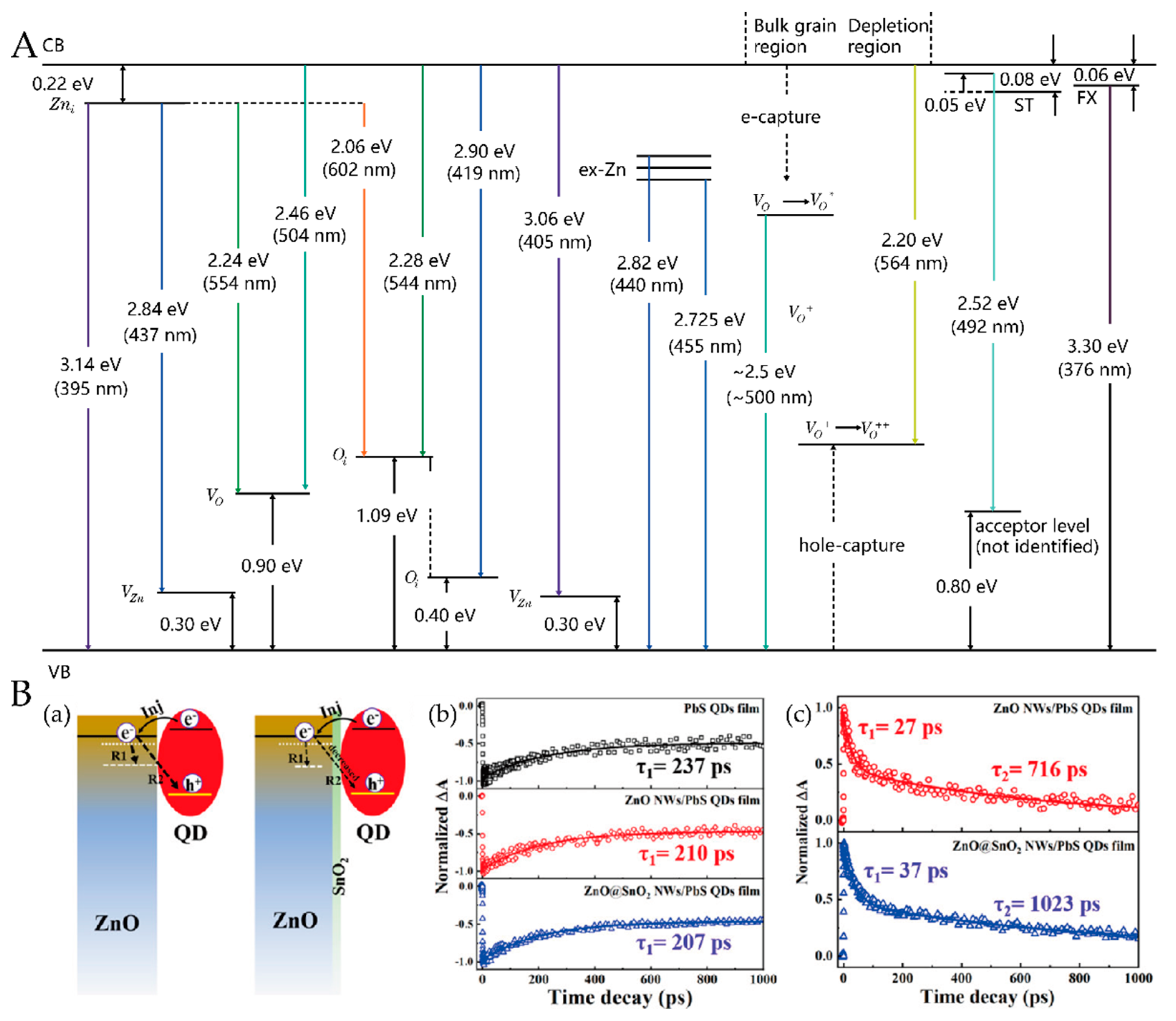
Figure 9. (
A) Energy level diagram showing some of the principal defect levels in ZnO [
101]; (
B) (
a) charge dynamic processes occurring at the ZnO NW/QD film interface. TA decay curves of the PbS QD film, ZnO NW/PbS QD film, and ZnO@SnO
2 NW/PbS QD film with a pump light of 470 nm and probe lights of (
b) 960 and (
c) 1500 nm [
104].
The defect concentrations of HT-grown ZnO NWs can be significantly reduced by annealing [
105]. Xu et al. [
106] successfully eliminated or passivated the defect-related PL emissions of ZnO NWs by employing sealed post-annealing treatment. Concerning again the surface defects of NWs, Kim et al. [
107] successfully reduced the number of excess-oxygen-related defects through thermal annealing in an
H2
ambient atmosphere above 300
℃. The excess-oxygen-related deep-level emissions were quenched completely, while the near band-edge emissions were greatly enhanced when H atoms were incorporated into ZnO NWs. These H atoms are most likely to exist in the form of shallow donors and may be removed after annealing at 400
℃ [
108,
109,
110]. Concerning the desorption of hydroxyl groups, Shi et al. [
108] confirmed that annealing at 150
℃ results in the removal of OH groups, but it may also introduce other hydrogen-related impurities. In a study of the overall performance of devices, Chang et al. [
86] found that 350
℃
might be the optimal annealing temperature, and the lowest defect emission and sufficient ZnO crystallinity were obtained at this temperature.
More recently, Tavakoli Dastjerdi et al. [
93] passivated ZnO NW surface states using the hydrogen plasma treatment. Compared with the untreated NWs, the PL spectrum of the H-plasma-treated ZnO NWs showed a clear enhancement of near-band emissions and a remarkable quenching of the visible emission peak. Through X-ray electron spectroscopy (XPS) analysis, the authors found an increase in the number of hydroxyl groups and attributed this to the passivated O-dangling bonds. Despite the increase in hydroxyl groups, reduced surface oxygen defects and possible H doping may lead to an improved overall performance [
93,
107]. Shi et al. [
35] obtained a 9.3% PCE by introducing ABA-modified ZnO NW arrays in QDSCs. In addition to the passivation of ZnO surface defect states, ABA modification can change the interfacial dipole momentum between ZnO NWs and CQDs, thus effectively increasing the vacuum level.
Parallel to the class of passivation strategies for post-annealing and surface treatment, depositing organic/inorganic coatings to passivate the surface of ZnO NWs were also investigated [
91,
109]. Zhang et al. [
104] clarified in detail the influence of surface
SnO2
passivation on the charge dynamic process in ZnO NWs by employing time-resolved photoluminescence (TRPL) and transient absorption (TA) spectroscopy techniques, as shown in
Figure 9b. After
SnO2 passivation, the PL intensity of the deep-level defects related emission clearly decreased and the time constants of the two recombination pathways (R1 pathway, in which free electrons are trapped by defect states, and the R2 pathway, in which free electrons are recombined with the holes of PbS QDs) increased, which confirmed the positive effect of the surface passivation layer. Interestingly, Zang et al. [
89] revealed the possibility of insulating interfacial modification with a Mg(OH)
2 interlayer; the performance of the IBHJ QDSCs improved, with a V
OC and PCE of 520 mV and 5.04%, respectively. Through the chemical reaction between ZnO and the TiO
2 precursor, Chang et al. [
86] fabricated
TiO2-passivated ZnO NW CQDSCs. They provided direct proof of the reduced recombination in the surface-passivated cell by transient open-circuit photovoltage decay measurements. The results showed that the
TiO2-passivated cells exhibited much slower decay processes than those of the bare unpassivated cells. More recently, Cheng et al. [
91] significantly minimized
VOC losses by passivating a ZnO nanowire surface with ALD
TiO2. Compared with unpassivated devices, the surface-passivated NW devices featured higher
Jsc and
VOC
, which was attributed to the passivated surface defects. The performance comparison before and after the passivation process can be seen intuitively in Table 4.
Table 4. Performance optimization of IBHJ QDSCs with passivation strategies.
| Passivation Strategy |
CQDSC Structure |
- |
Jsc (mA/cm2) |
Voc (mV) |
FF |
PCE (%) |
| H-plasma-passivation [93] |
ITO/ZnO NWs/PbS-TBAI/PbS-EDT/Au |
non-treated |
30.0 |
591 |
0.56 |
9.9 |
| H-plasma treated |
31.1 |
610 |
0.57 |
10.8 |
| ABA-passivation [35] |
ITO/ZnO NWs/PbS-TBAI/PbS-EDT/Au |
non-treated |
27.4 |
510 |
0.60 |
8.41 |
| ABA-treated |
27.5 |
540 |
0.64 |
9.52 |
| Mg(OH)2 [89] |
FTO/ZnO NWs/PbS-TBAI/PbS-EDT/Au |
without Mg(OH)2 |
22.62 |
390 |
45.66 |
4.03 |
| with Mg(OH)2 |
21.51 |
520 |
45.08 |
5.04 |
| SnO2 [92] |
FTO/ZnO NWs/PbS-CTAB/Au |
without SnO2 |
20.4 |
580 |
0.47 |
5.55 |
| with SnO2 |
23.2 |
603 |
0.56 |
7.78 |
| CBD-TiO2 [86] |
FTO/ZnO NWs/PbS-CTAB/Au |
without TiO2 |
28.7 |
279 |
0.430 |
3.50 |
| with TiO2 |
30.7 |
420 |
0.478 |
6.16 |
| ALD-TiO2 [91] |
FTO/ZnO NWs/PbS-TBAI/PbS-EDT/Au |
without TiO2 |
25.3 |
505 |
0.54 |
6.9 |
| with TiO2 |
26.0 |
497 |
0.56 |
7.2 |
4.3. Other Optimization Strategies
The effective infiltration of QDs in NW arrays is an important means of reducing interfacial defects. However, an important fact is that IBHJ QDSCs may feature a large number of voids, and these voids could cause a sharp decline in the performance of devices. Recently, more and more evidence has shown that the deposition method exerts an important effect on the morphology of thin films. Although the traditional spin-coating deposition method features advantages in small-scale fabrication due to its simplicity and practicability, it may be difficult to control the morphology due to the uneven shear stress distribution during the coating process [
86]. In addition, it is still debatable whether mechanical fractures occur in the process of high-speed rotation of NW arrays, which aggravate the deterioration of the performance. A new deposition method based on the meniscus was proposed. “Meniscus-guided” means that the meniscus is shifted across the substrate by a coating head or viscous force to effectively guide and control film deposition [
110]. Due to the inherent directivity of the coating process, the QDs can be effectively deposited by penetration. This method is appropriate for large-scale use. By simultaneously controlling the growth orientation of the NWs and introducing convective assembly as the CQD deposition technique, the dense packing and efficient infiltration of CQDs can be effectively improved. In this way, Shi et al. produced a finely interpenetrating OBHJ structure between ZnO NW arrays and PbS CQDs, and demonstrated a PCE of 9.92% in the devices [
35].
QDSC design for stability is also an important subject for PV commercialization. Without considering the NW light aggregation effect and similar structural issues, IBHJ QDSCs are similar to planar QDSCs in that their device lifetime is mainly dependent on the QD material itself. Current synthesis and defect passivation techniques have been effective in reducing the oxidation sites associated with the stability of materials. PbS QDSCs can maintain their initial PCE in air with no encapsulation for 30 days [
108]. In another study, ZnO NW-based CQDSCs exhibited excellent stable properties (the PCE was almost constant) after being stored in air for 250 days [
92]. Further stability optimization strategies need to consider the mechanism of ambient factors (such as oxygen, water, and increased temperatures or high intensities of illumination) affecting the QDs. The intrinsic properties of the QDs themselves and their interplay with other materials are also factors to be considered [
110].
3. Conclusions
IBHJ QDSCs form a 3D depletion region for the high-efficiency utilization of solar energy, which allows the incorporation of more QD material while maintaining efficient charge collection. As ETLs, ZnO NW structures should offer optimal electric continuity and need to be relatively transparent to visible light to avoid photon loss. In this study, an assessment was performed on the previous research into the preparation of ZnO NWs, and the effect of the ZnO NW morphology on performance and the optimization strategies of IBHJ QDSCs were summarized. The conclusions and outlooks are as follows:
- (1) The HT method is more suitable for the large-scale application of IBHJ QDSCs due to its advantages of low temperature, high yield, and easy processing. The morphology of HT-grown NWs is influenced by the seed layer properties, growth time, concentration, temperatures, PH, and post-treatment conditions. However, it is necessary to investigate the mechanism of these influencing factors for the preparation of NWs with controllable morphologies. Furthermore, the optimization of surface defects and internal defects and the reliability of HT-doping elements also need to be studied further to improve the performance of the ETL and to tune the band-gap arrangement.
- (2) The density of the NW affects the filling volume of QD materials. High-density NW arrays not only feature a large VOC loss due to their large interface area, but also cause high reflectivity in the SCs, reducing the light absorption. The length of the nanowires determines the depth of the carrier collection and further affects the thickness of the SCs. However, long NWs often result in poor hole collection and increase the interface area. In addition, the length of the nanowires affects the light trapping effect of the 3D structure, and may cause the aggregation of light absorption and ultimately affect the recombination of the carriers.
- (3) The geometric morphology of the NW exerts a great influence on the transmission and collection of photocarriers. The optimization of NW spacing needs to take account of the transverse collection of electrons, while the length of the NW and the thickness of the SC absorption layer need to be determined after comprehensively analyzing the longitudinal aggregation of holes. In order to satisfy the carrier collection conditions as far as possible, reducing the NW density can increase the filling volume of QD light absorption material.
- (4) In order to further optimize the 3D structure, more accurate carrier transport mechanism analysis needs to be carried out in combination with electrical simulation to determine the optimal electrical structure. The light-trapping effect caused by NWs also needs to be more accurately analyzed, since poor light scattering may lead to local light aggregation and thus affect the distribution and collection efficiency of photocarriers.
- (5) The passivation of the NW surface is an important way to improve the VOC of IBHJ QDSCs. Passivation strategies commonly include post-annealing, H-plasma treatment, and ABA surface treatment. Moreover, the addition of Mg(OH)2, SnO2, and TiO2 buffer layers on the surface of NWs also effectively improves the performance of SCs. However, the effects of the passivation layer (including the passivation mechanism of the defects and the band arrangement of the battery) on the three-dimensional heterojunction remain to be explored. A comparative study of different passivation layers may be helpful in this regard.
This entry is adapted from the peer-reviewed paper 10.3390/nano12010114