Your browser does not fully support modern features. Please upgrade for a smoother experience.
Please note this is an old version of this entry, which may differ significantly from the current revision.
Sensors based on single-photon avalanche diodes (SPADs) are nowadays employed in a wide variety of single-photon counting and fast-timing applications, e.g., high-energy physics; time of flight (TOF) ranging and 3D imaging; Raman spectroscopy; and bio-medicine, including fluorescence-lifetime imaging microscopy and positron emission tomography (PET), to name a few. SiPMs are the most common sensors in PET applications, where they detect the light produced by the interaction between gamma photons and scintillator crystals.
- silicon photomultipliers
1. Introduction
Sensors based on single-photon avalanche diodes (SPADs) are nowadays employed in a wide variety of single-photon counting and fast-timing applications, e.g., high-energy physics [1,2]; time of flight (TOF) ranging and 3D imaging [3]; Raman spectroscopy [4]; and bio-medicine, including fluorescence-lifetime imaging microscopy [5,6] and positron emission tomography (PET) [7,8,9], to name a few. When implemented in CMOS image sensor technologies, SPAD sensor architectures benefit from the combination of per-pixel and per-chip processing and control circuitry with good-enough photodetectors [7,10,11]. Particularly, as Figure 1 illustrates, digital SiPMs employ micro-cells consisting of SPADs and embedded processing circuitry to directly encode SPAD avalanches into digital values, thus providing large flexibility for system implementation [12].
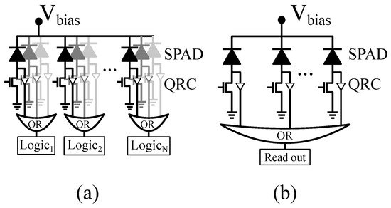
Figure 1. (a) Segmented digital silicon photomultiplier (SiPM) and (b) digital SiPM with common readout.
SiPMs are the most common sensors in PET applications, where they detect the light produced by the interaction between gamma photons and scintillator crystals, as it is schematically shown in Figure 2. Even though for this analysis, we will focus on monolithic crystal blocks attached to an array of SiPMs [13], the issues encountered for this configuration can be partially extrapolated to detectors consisting of pixelated crystals [14,15,16,17]. For a monolithic crystal, the scintillation photons are spread all over the array and, as a result, the amount of photons over each sensor is relatively small. These optical photons contain information about the arrival time of the incident particle, the energy transfer to the crystal, and the first interaction point within the crystal. Therefore, it is essential to maximize their detection to improve the reconstruction of the gamma event and, ultimately, the quality of the PET image.
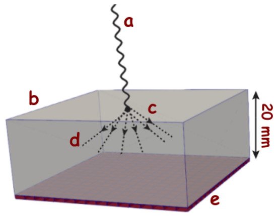
Figure 2. Schematical representation of an incident gamma ray (a) that interacts with a scintillating crystal (b) of typical size (50 × 50 × 20 mm2) at the point (c), producing optical photons (d) (which are of the order of 105/MeV depending on the crystal) that are detected by the photodetector placed at (e) that is optically coupled (i.e., with optical grease) to the scintillator.
For pixelated crystal detector configurations, the intrinsic spatial resolution is determined by the pixel’s size. However, as the gamma photon normally suffers from Compton scattering before being totally absorbed, the optical photons are spread over more than one SiPM pixel, similar to the previous case. Hence, for this configuration also, we need a good timing resolution in order to determine the first interaction point and reduce the Compton noise that affects the resolution of the reconstructed medical image. In addition, both pixelated and monolithic detectors require good timing resolution to achieve satisfactory coincidence time resolution (CTR) and enable the inclusion of TOF information for PET scanners. This can be achieved with a smaller SiPM pixel size with independent TDCs.
2. Trade-Offs in SiPM Design for PET and SPECT
For PET and SPECT imaging, one needs to reconstruct the interaction point in the scintillating crystal. However, before a gamma ray is totally absorbed through a photoelectric effect, it usually undergoes previous Compton scattering in a non-negligible percentage of cases. In Figure 3, we see (from a Monte Carlo simulation) a typical example of Compton scattering (C) previous to a photoelectric absorption (P). Ideally, in order to perform an accurate image reconstruction, one would need to extract the first interaction point (C). However, with current technology, this is a rather challenging task, and the estimated interaction point normally corresponds to the center of mass (CM) of the energy distribution of the optical photon readout. A good timing resolution together with an independent timestamp readout of each pixel would allow us to disentangle the two interactions and their chronological order and therefore recognize the first interaction point. We shall briefly comment on these aspects in the following paragraphs.
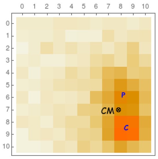
Figure 3. Representation of a 10×10 matrix of 1 × 1 mm2 pixels (coupled to a scintillating crystal as in Figure 2, but with a smaller size) for a typical event with a Compton interaction (C) previous to a photoelectric absorption (P). The electronic readout normally associates the coordinates of this gamma ray event to the center of mass of the energy distribution (CM). Higher-intensity colors correspond to a higher number of detected optical photons.
The spatial resolution and sensitivity of molecular imaging scanners, such as PET or SPECT, has been drastically improved by reducing the SiPM sizes down to 1 × 1 mm2, reaching depth resolutions down to 0.7–0.8 mm for tomographic images, corresponding to small animal PETs used for pre-clinical applications [18,19]. However, an even bigger challenge is to provide such scanners with a better time resolution and to incorporate TOF information in the image reconstruction algorithm even for standard PET scanners. This can further improve the resolution of the final reconstructed image [20,21], which in turn would allow a patient dose reduction—and all the associated benefits to a lower exposure to gamma ray radiation. Improving the time resolution also helps distinguishing the first interaction point of the gamma photon to push the limits of the depth scanner resolution. This is achieved by reducing the random events leading to false PET coincidences, and the Compton noise represents the gamma ray interactions that take place in the scintillator crystal before it is finally absorbed through a photoelectric effect.
Generally, during the design of SiPMs for single-photon counting applications, such as PET and Čerenkov Telescopes, the photon detection efficiency (PDE) is chosen as a driving figure of merit (FOM). Since PDE is the product of the PDP and the fill factor, designers are forced to implement SPAD pitches from 30 to 60 μm—while keeping the quenching and logic area as small as possible—to achieve fill factors ranging from 50 to 70% [7,22] in order to maximize light detection. The use of PDE as a reference in PET-TOF scanners is further motivated by the fact that the uncertainty in determining the arrival time of the gamma photon is strongly limited by the number of detected photons rather than being dominated by the SPAD jitter or the single shot precision of the time to digital converter (TDC) [23,24]. Despite the relevance of the active area for these sensors, the fill factor losses due to defective SPADs—the ones that must be turned off due to their noise—are not usually considered during the design. This leads to an overestimation of the actual PDE in digital SiPMs.
This entry is adapted from the peer-reviewed paper 10.3390/s22010122
This entry is offline, you can click here to edit this entry!