Because of having high aspect ratio nanowires(NWs) structures offer great advantages in many sensing and biological systems. Magnetic/non-magnetic multilayered NWs were fabricated by electrochemical deposition, usually by using potentiostatic, galvanostatic techniques, and they were seen to be kinetic or diffusion control. By using optimized deposition parameters i.e presence of additives, potential, solution concentration, hydrogen evolution and confinement effect of nanopore wall, one can successfully fabricate NWs with well-defined segmented structures for single, bilayer or even tri layer thickness. Structural and chemical compositional of the multilayer NWs was observed by using various characterization techniques i.e electron microscopy, spectroscopy, and x-ray diffraction. Studying the kinetics of the phase transformation of NWs between stable or metastable phases reveals basic thermodynamical information and essential for future various applications.
- electochemical deposition
- multisegmented nanowires
- transmission electron microscopy
It is clear from the previous research work that the deposition parameters affects the growth mechanism of metal NWs, and it has technological and fundamental interests. The studies of Tian et al. [112] showed two important points: (1) At low deposition potential Cu, Ag and Au are single crystalline with preferred orientation [110], having an fcc structure, and using high deposition potential polycrystalline structure was obtained; (2) the Ni NWs have a polycrystalline nature and are rather insensitive to deposition potential. They explained that, at lower deposition potential larger critical nuclei are formed, which helped in formation of single crystalline NWs. However, Pan et al. [113] formed single crystalline Ni NWs using high deposition potential, with preferred orientation along [109] direction, they explained that the adsorption of H adatoms on cathode favors [109] growth orientation. Likewise, some other research groups claimed that the electrolyte pH (i.e., from 2 to 6) has no effect on orientation of Ni NWs [114,115]. The formation of fcc Ni, and Ag NWs along [109] was also observed by other researchers [116–118]. The growth of single crystalline metal NWs was very well demonstrated by Tan Ming and Xinqi Chen [119]; according to them, the growth of single crystalline NWs occurs on atomically rough planes like hcp [1010] and fcc [110] rather than smooth planes like hcp [0001] and fcc [111]. The reason for this is because the sites for dehydration on atomically rough planes are larger in number than smooth planes [119]. The change in phase transformation of Co NWs was seen (i.e., from hcp to fcc) by changing the deposition parameters [120–122], and a group of studies by Mukhtar et al.[123–127] showed that the smaller grain size of Co favors the formation of fcc Co NWs, and larger grain size favors the formation of hcp Co NWs. Similarly, the mixture of hcp and fcc phases was observed in Co NWs, which seems to crystallize in early stage of deposition, and later with the increase in deposition time as the length of Co NWs increases, they crystallize into the hcp phase [128]. Wang et al. [129] studied the expansion behavior of hcp Co NWs arrays along the (1010) plane and fcc Co NWs arrays along the (220) plane. The amount of change in the interplanar spacing of the hcp Co NWs array was found to be larger than the variation in the interplanar spacing of the fcc Co NWs array. The ability to control the thermal expansion of Co NWs is expected to provide new opportunities for the design of magnetic nano-devices.
By having the knowledge of growth of single NWs, as explained in the paragraph above, one can likely understand the growth of multilayer nanostructure. As mentioned in Table 2, the current density, potential and pulse time are the important parameters to form the distinct interface of multilayer NWs, and by controlling these parameters a distinct interface of multilayers could be formed. XRD is a significant tool to study the coherence in multilayers, because if they are coherent there are a lot of them to produce a strong Bragg diffraction peak. Satellites should appear on both sides of Bragg diffraction in the case if the structures are supper-lattice as shown in Figure 6a [130]. The angular shift between the satellites and the Bragg diffraction peak can be explained by , where λ is the wave length of X-ray photon, and Δθ is the angular shift, and Λ is the periodicity of superlattice structure. The main peak was seen as intermediate between the diffraction peaks for Ni and Cu, and satellites can specify that the thickenss of the layers are nearly equal, and they are reproduced by repeating the same experimental conditions cycle by cycle [130]. A lot of work has been done recently on Ni, Co, Fe, Pt and their alloys with Au, Ag, Cu segments [131–134]. High resolution TEM images allow us to study the cross sectional shape of NWs, which is absoultely cylindrical, but in some studies it deviate from the original shape due to defects in the porous template (Figure 6b,c). Advanced SEM intruments like the Zeiss ULTRA 55 [96] are able to detect the interface defects of multi-segments very clearly, as shown in Figure 6d,e. Both energy-dispersive X-ray spectroscopy (EDS) and energy loss spectroscopy (EELS) gives the chemical composition NWs. The EDS mapping in TEM provides better and higher spatial resolution than the EDS in SEM, and EELS technique even gives more detailed chemical mapping about nanostructure [95,135]. Scanning transmission electron microscopy(STEM) with high angle annual dark field detector depends on material atomic number under study, as the atomic number of magnetic segment (Co) is lower than non-magnetic segment (Au), the magnetic segment appears darker and non-magnetic layer appear as a bright segment (see Figure 2a of [136]). Further analysis of High resolution transmission electron microscopy (HRTEM) showed the polycrystalline nature of Co-Au multilayers, and the growth orientation of Co was interestingly different on [011] and [002] at both sides between Au [210] plane [136]. Figure 7a show the SEM image of CoFe/Au/CoFe NWs, and Figure 7b,c,d show the EDX mapping of Co, Fe and Au NWs. Similarly, the phase change occurred in NiFe-Au multilayers NWs in NiFe segment from fcc to bcc as the concentration of Fe ions in solution increases [134,137], and for Ni30Fe70/Cu NWs the increase in Cu thickness from 4 nm to 12 nm and the phase change from bcc (110) to fcc (111) was observed [138].
Co-Cu is the most studied system among the tailored multilayerd nanostructures. According to previous studies[1] [2]the direct-current deposition of Co-Cu alloy results in to mixture of fcc and hcp phase, while pulse deposition of multilayered CoCu/Cu films the dominant fcc phase was obtained with little hcp crystals(>2%). Cziraki et al.[3] studied the structural evolution in CoCu/Cu films, study show that at the initial time of deposition nano-size small hcp and fcc crystallites was formed with high internal stress, after this initial polycrystalline region the size of crystals increases, and finally a fcc super-lattice columnar structure was formed. During the deposition process the bending of layer was observed[4], this bending of layers was also observed by the Co/Au and Co/Pd multilayers[5]. While studying NiCo-Cu NWs same phenomena was observed by S. Zsurzsa et al.[6], authors suggested that the bending may occur because of the restricted growth of NWs inside the pore wall, which may act as the grain boundaries, as the interface do in the columnar growth, which results in convex curvature. Meanwhile, depositing the multilayer Co-Cu NWs, the control over deposition parameters, the fcc phase of multilayer NWs was formed [120,139–141], which is highly desirable for magnetic applications. 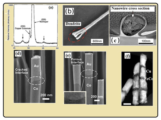
Figure 6. (a) X-ray diffraction image of Ni-Cu multilayer composite and two downward arrows with the main central peak show the typical satellites of Ni-Cu multilayer. Reprinted with permission from [130] Copyright “Elsevier”, (b) SEM image of NW with dendrite structure, (c) Transmission electron microscopy (TEM) image show the cross section of NW. Reproduced from Reference [142] used in accordance with the Creative Commons Attribution (CC BY 4.0) license, (d,e) SEM of Co-Au NWs shows the defected interface of Co and Au, indicated the porous and cracked interface. Reprinted with the permission from [96] Copyright (2014) “American Chemical Society”, (f) Scanning transmission electron microscopy (STEM) image of FeCo-Cu. Reprinted with the permission from [102] Copyright (2015) “American Chemical Society”.
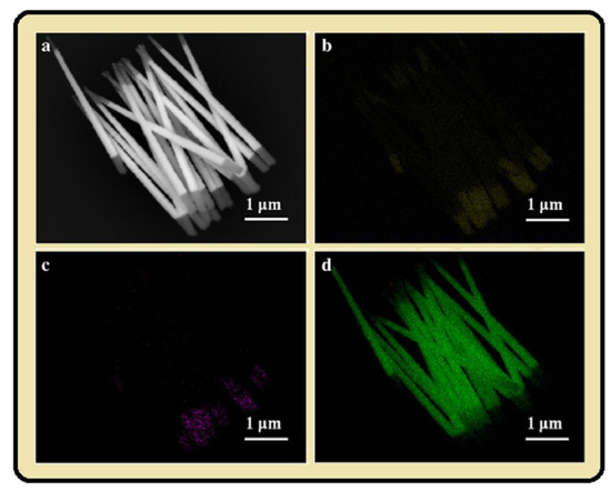
Figure 7. (a) SEM image of CoFe/Au/CoFe NWs, EDX mapping of (b) Co, (c) Fe, and (d) Au concentration. Reprinted with permission from [143] Copyright (2013) “Elsevier”.
This publication can be found here:https://www.mdpi.com/1996-1944/12/23/3908
References
- S. Zsurzsa; E. Pellicer; J. Sort; L. Péter; I. Bakonyi; Electron Microscopy Characterization of Electrodeposited Homogeneous and Multilayered Nanowires in the Ni-Co-Cu System. Journal of The Electrochemical Society 2018, 165, D536-D542, 10.1149/2.0571811jes.
- Á. Cziráki; L. Peter; B. Arnold; J. Thomas; H.D. Bauer; K. Wetzig; I. Bakonyi; Structural evolution during growth of electrodeposited Co–Cu/Cu multilayers with giant magnetoresistance. Thin Solid Films 2003, 424, 229-238, 10.1016/s0040-6090(02)01126-4.
- L. Peter; Z. Kupay; Á. Cziráki; J. Pádár; J. Toth; I. Bakonyi; Additive Effects in Multilayer Electrodeposition: Properties of Co−Cu/Cu Multilayers Deposited with NaCl Additive. The Journal of Physical Chemistry B 2001, 105, 10867-10873, 10.1021/jp011380t.
- Á. Cziráki; L. Peter; B. Arnold; J. Thomas; H.D. Bauer; K. Wetzig; I. Bakonyi; Structural evolution during growth of electrodeposited Co–Cu/Cu multilayers with giant magnetoresistance. Thin Solid Films 2003, 424, 229-238, 10.1016/s0040-6090(02)01126-4.
- F. Hakkens; W. Coene; F.J.A. Den Broeder; Micro- and Nanostructure of Co/Pd and Co/Au Multilayers Studied with Transmission Electron Microscopy. MRS Proceedings 1991, 231, 397-404, 10.1557/proc-231-397.
- L. Péter; A. Cziráki; L. Pogány; Z. Kupay; I. Bakonyi; M. Uhlemann; M. Herrich; B. Arnold; T. Bauer; K. Wetzig; et al. Microstructure and Giant Magnetoresistance of Electrodeposited Co-Cu/Cu Multilayers. Journal of The Electrochemical Society 2001, 148, C168-C176, 10.1149/1.1346606.
- F. Hakkens; W. Coene; F.J.A. Den Broeder; Micro- and Nanostructure of Co/Pd and Co/Au Multilayers Studied with Transmission Electron Microscopy. MRS Proceedings 1991, 231, 397-404, 10.1557/proc-231-397.