Your browser does not fully support modern features. Please upgrade for a smoother experience.
Please note this is an old version of this entry, which may differ significantly from the current revision.
Subjects:
Nanoscience & Nanotechnology
With the rise of topological insulator samarium hexaboride (SmB6), rare-earth hexaboride (RB6) nanowires are the focus of the second wave of a research boom. Recent research has focused on new preparation methods, novel electronic properties, and extensive applications.
- nanowire
- field emission
- chemical vapor deposition
1. Introduction
Rare-earth hexaborides (RB6) have received substantial attention thanks to their high electrical conductivity, high melting points, and high chemical stability. Meanwhile, the strong correlation effect of 4f–5d electrons of rare-earth elements also brings some newfangled physical properties of RB6 [1,2,3]. For example, yttrium hexaboride (YB6) is a superconductor with a Tc of 7.2 K, which is the second highest transition temperature among all borides [4]. Moreover, lanthanum hexaboride (LaB6), possessing low work function of 2.7 eV, is a famous thermionic electron emission material with high current density and stability [5]. Cerium hexaboride (CeB6) is an antiferromagnetic heavy-fermion metal, but recently, it was found to demonstrate low-energy ferromagnetic fluctuation [6]. Furthermore, as a ferromagnetic semimetal, europium hexaboride (EuB6) recently exhibited a colossal magnetoresistance effect [7]. In recent years, the emergent topological insulator has increased interest in samarium hexaboride (SmB6), which possesses both insulating bulk state and metallic surface state due to the inversion of the d and f bands. Experimental evidence proves that SmB6 is the first strongly correlated 3D topological Kondo insulator [8].
Due to the small size effect and quantum confinement effect, one-dimensional (1D) nanomaterials have new properties compared with bulk crystals. With the rise of 1D nanomaterials, RB6 experienced the first wave of a research boom from 2005 to 2015, and many RB6 nanowires were prepared by chemical vapor deposition (CVD) [9,10,11,12,13,14,15,16,17,18,19,20]. These RB6 nanowires achieved excellent field emission properties and mechanical properties [21,22,23,24,25,26,27,28,29]. From 2016, the second wave of research boom of RB6 began as SmB6 proved to be a topological insulator, and researchers began to explore the difference in topological properties between nanowires and bulk single crystals [8].
2. Properties and Applications of RB6 Nanowires
2.1. Electronic Transportation
As an emerging topological insulator, many experiments and theoretical studies have been conducted on bulk SmB6 single crystals [8]. From 2016, researchers began to investigate the novel electronic transport and magneto-transport properties of SmB6 nanowires [37,38,53,58,59,60,61,62]. In 2017, Kong et al. reported the spin-polarized surface state transport of single SmB6 nanowires (Figure 1a–c) [58]. Under 5 K, the resistance appears saturated and flat, indicating that the surface states control the transport behavior. The appearance of topological surface states is caused by the reversal of d and f electrons. The fitting of a temperature-dependent resistance curve reveals that SmB6 nanowire has a bulk gap ~3.2 meV, which is opened by the hybridization of the 4f bands and 5d bands in SmB6 nanowires. As shown in Figure 1c, the magnetoresistance (MR) of SmB6 nanowires is negative and the MR shows no sign of saturation at high magnetic field up to 14 T. The negative MR indicates that this transport behavior is spin-dependent. Furthermore, the nonlocal tests reveal that the surface state transport of SmB6 nanowires is spin-polarized. In another interesting work, Zhou et al. reported the positive planar Hall effect (PHE) of SmB6 nanowires (Figure 1d–f) [59]. They found that as the temperature decreases, the amplitude increases sharply, but saturates at 5 K. This positive PHE is due to the surface states of SmB6. In other studies, the researchers found the anomalous magnetoresistance and the hysteresis of magnetoresistance in SmB6 nanowires [60,61,62].
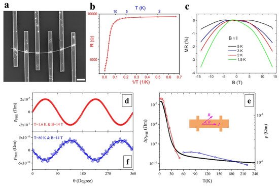
Figure 1. (a) SEM image of a SmB6 nanowire device, the scalebar is 2 μm. (b) Temperature-dependent resistance of the SmB6 nanowire. (c) Magnetoresistance curves under a parallel magnetic field at various temperatures [58]. Copyright 2017, American Physical Society. (d) Planar Hall resistivity with various angles at 1.6 K. (e) PHE amplitude and resistivity. Inset is the definition of tilting angle θ. (f) Planar Hall resistivity with various angles at 80 K [59]. Copyright 2019, American Physical Society.
In the RB6 family, like SmB6, YbB6 is proposed to be a mixed-valent (Yb2+/Yb3+) topological insulator and demonstrates new quantum phenomena [63,64,65]. In 2018, Han et al. reported the semiconductor–insulator transition behavior in a YbB6 nanowire (Figure 2) [55]. As shown in Figure 2b, as the temperature decreases from 300 to 2 K, the resistivity of the YbB6 nanowire device undergoes a dramatic 49-fold increase (ρ2 K/ρ300 K = 49). They propose that the semiconductor–insulator transition is due to a small band gap opening at a low temperature induced by the slightly boron-rich or boron-deficient segments in YbB6 nanowires. Furthermore, the magnetoresistance (MR) of the YbB6 nanowire was tested with perpendicular magnetic field B = 0–7 T at various temperatures. As displayed in Figure 2c, the MR shows no sign of saturation at high magnetic field up to 14 T and has a linear dependence with B2 at 2 K and 10 K, which follows Kohler’s law. Because a semiconductor–insulator transition occurred at 2 K for YbB6 nanowires, the hole-dominant transport is credible at 2 K and the transport at 10 K is electron-dominant.
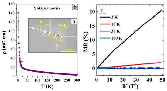
Figure 2. (a) SEM image of the YbB6 nanowire device. (b) Resistivity as a function of temperature from 2 to 300 K. (c) Magnetoresistance (MR) as a function of B2 at various temperatures [55]. Copyright 2018, Elsevier Science B.V.
Of all the metal borides, YB6 bulk crystals have the second highest superconducting transition temperature of 7.2 K after MgB2. More superconducting properties have been studied in bulk YB6 single crystals, but the superconducting properties of YB6 nanowires have not been reported. Recently, Wang et al. reported the synthesis of 1D YB6 nanowires by a high-pressure solid-state method and studied their magnetic properties (Figure 3). The temperature-dependent magnetization under zero-field cooling and field cooling revealed that the YB6 nanowires have a superconducting transition with Tc = 7.8 K. Meanwhile, they found that the YB6 nanowires exhibited a peak effect in the superconducting state observed from the magnetic hysteresis loops obtained at 2 K and 10 K, indicating that YB6 nanowires pertain to a type-II superconductor.
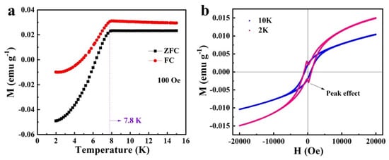
Figure 3. (a) The temperature-dependent magnetization under zero-field cooling and field cooling modes of superconducting YB6 nanostructure. (b) The magnetic hysteresis loops obtained at 2 K and 10 K [57]. Copyright 2021, Elsevier Science B.V.
LaB6 bulk single crystals have been applied in commercial scanning electron microscopy and transmission electron microscopy. For RB6 nanowires, the most attractive application is also the field emitter of an electronic gun of an electron microscope (Figure 4) [66,67,68]. Published in Nature Nanotechnology, Zhang et al. reported the first application of a single LaB6 nanowire to scanning electron microscopy, revealing excellent performance [66]. Their LaB6 nanowire electron source shows low work function, is chemically inert, and has high monochromaticity. When assembled into a field-emission gun of SEM, it demonstrates ultra-low emission decay, and its current density gain is three orders of magnitude higher than traditional W tips. By this LaB6 nanowire-based SEM, they obtained low-noise and high-resolution images, better than W-tip-based SEM. Recently, published in Nature Nanotechnology in 2021, Zhang et al. reported the installation of a single LaB6 nanowire into an aberration-corrected transmission electron microscope [67]. The LaB6 NW-based TEM achieved atomic resolution and probe-forming modes at 60 kV energy. Compared with the state-of-the-art W (310) electron source, the nanostructured electron source provides higher temporal coherence at a spatial frequency of 105 pm, showing a higher contrast transfer amplitude of 84% and a spectral energy resolution of 35%. The first demonstration of the LaB6 nanowire electron source in SEM and TEM reveals that the RB6 nanowires have notable application prospects and commercial value both in electron microscopy and other electron-emitting devices.
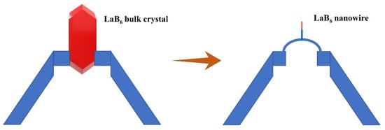
Figure 4. Illustrations of the LaB6 bulk crystal and nanowire electron-emission sources in electron microscopy.
2.2. Optoelectronic Properties
Most of the RB6 crystals are metals with zero band gap, and thus, they are not suitable for semiconductor devices, such as field effect transistors and photodetectors. However, as a topological Kondo insulator, SmB6 shows a small gap (3 meV), evidenced by electrical transport measurements, and may have potential in fabricating devices. Recently, Zhou et al. [69] first reported the self-powered SmB6 nanowire photodetectors with broadband wavelengths covering from 488 nm to 10.6 μm (Figure 5). They claimed that the photocurrent stemmed from the interface of SmB6 nanowire and Au electrodes owing to the built-in potential, proved by the spatially resolved photocurrent mapping. The current on/off ratio, responsibility, and specific detectivity are 100, 1.99 mA/W, and 2.5 × 10⁷ Jones, respectively. The demonstration of a SmB6 nanowire photodetector reveals its application potential in mid-infrared photodetectors.
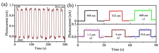
Figure 5. (a) Current–time measurement of SmB6 nanowire photodetector under illuminating of 10.6 μm light source. (b) Current–time curves of SmB6 nanowire photodetector under illuminating with different light wavelengths [69]. Copyright 2018, AIP Publishing.
2.3. Electrochemical Performances
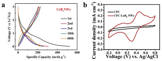
RB6 crystals show excellent metal-like conductivity (>103 S m−1) and they are suitable for active electrochemical electrode materials for energy storage. Recently, Wang et al. [52] reported the application of CeB6 nanowires as lithium-ion battery anode materials, and they obtained a capacity of ~225 mA h g−1 after 60 cycles (Figure 6a). The kinetic analysis shows that the Li+ storage mechanism mainly comes from the surface capacitive behavior. Xue et al. [70] reported the LaB6 nanowires on carbon fiber as electrode materials for supercapacitors (Figure 6b). The LaB6 electrode materials showed a high areal capacitance of 17.34 mF cm−2 and revealed suitable cycling stability after 10,000 cycles. The successful application of RB6 nanowires in batteries and capacitors demonstrates their potential in the field of electrochemical energy storage.
This entry is adapted from the peer-reviewed paper 10.3390/su132413970
This entry is offline, you can click here to edit this entry!