Your browser does not fully support modern features. Please upgrade for a smoother experience.
Please note this is an old version of this entry, which may differ significantly from the current revision.
Subjects:
Energy & Fuels
An evaluation of the degradation effects on photovoltaic modules is essential to minimise uncertainties in the system operation. Bifacial photovoltaic technology is attracting attention due to the capacity of generating energy from the front and rear sides. The term degradation is defined as a gradual deterioration of the characteristics of a material, component, or system. This deterioration may cause an impact on the system capacity to operate within the expected limits and therefore impact directly on their operating conditions.
- degradation
- photovoltaic
- PV losses
- Mismatch
- PV
- Solar Energy
1. Encapsulant Discoloration and Delamination
C-Si PV modules correspond to the largest proportion of the market share worldwide, occupying a total of 95% [1]. These modules are composed of a front glass, solar cells, and metal contacts involved by a polymeric encapsulant and a back sheet. The module encapsulant places an important role in the bonding multiple layers that compose a PV module. This encapsulant must have high optical transmittance, provide good adhesion to the different materials within a PV module, and have the capability to support mechanical stress due to expansion caused by different thermal coefficients, as well as good dielectric properties [2]. These characteristics are essential to improve the solar irradiance reaching the PV cell’s surface and the resilience of the PV module exposed to outdoor conditions. In the PV market, Ethyl Vinyl Acetate (EVA) is the most used encapsulant material due to its low cost and high thermal stability [3]. This material has the disadvantage of yellowing or browning when exposed to UV light and high temperature for a long period [2]. This change in the color impacts the material transmissivity and reliability of the PV module as described in Figure 1.

Figure 1. Encapsulant discoloration causes and effects [4].
One of the initial effects is the reduction of the transmissivity of the encapsulant caused by the change of the encapsulant color as represented in Figure 2b. This effect occurs when the module is exposed to UV radiation and temperatures above 50 ∘C [5]. The intensity of the discoloring varies from yellow shade, brown, and dark brown. This discoloration impacts the amount of solar irradiance that reaches the surface of the solar cell. As a consequence of the lower irradiance levels, the short-circuit current Isc of the cell/module reduces, as seen in the I-V curve in Figure 3. impacting directly on the module’s efficiency [3][4].
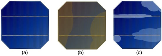
Figure 2. Degradation of PV module. (a) Ideal cell, (b) Discolouring effect, (c) Delamination effect.
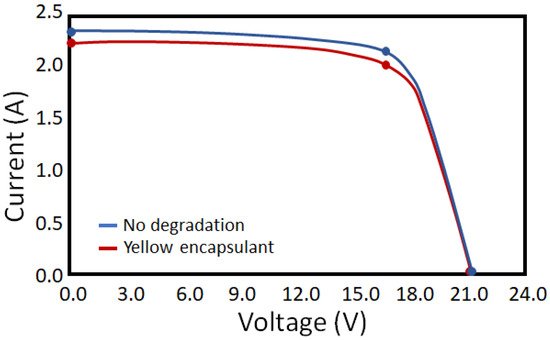
Figure 3. Encapsulant degradation effect on I-V curve [6].
Another problem caused by the degradation of the encapsulant results in a chemical effect. In the degradation process of the EVA, acetic acid and other volatile gases are produced. These gases get trapped within the layers of the PV module, creating bubbles and causing the delamination of the layers as represented in Figure 2c. This impacts significantly on the performance, safety, and reliability of the PV module. Additionally, acetic acid causes corrosion of the metallic contacts of the solar cells, which increase the losses due to the increase of the module’s series resistance (Rs) [4][7]. The change in colour of the encapsulant and the appearance of bubbles, delamination, and corrosion, do not appear evenly on the surface of the module.
For partially yellowed modules, the short-circuit current showed a reduction of 6–8% below the nominal value; while for complete yellowed modules, the short-circuit current can be from 10 to 13% less than the nominal value. Consequently, the module maximum power is also reduced according to the intensity of the discolouring [6] as seen in Figure 3.
Indoor tests performed on bifacial cells without the encapsulant and exposing the front and rear side to the same irradiance levels, showed that the rear side passivation layer is more sensitive to UV light than the front side. In PERC type cells, the degradation caused a significant drop in the Isc [8]. The power loss of the rear side showed to be 2.4% per year while the front side only 1.4% per year [8]. Although, with EVA encapsulant and outdoor conditions, the front side of the module receives a higher dose of irradiance compared to the rear side. Albadwawi et al. [9] found that in extreme desert conditions, the front side discoloration can cause a degradation of 1.3–1.88% per year while for the rear side, this degradation is around 0.39–0.78% per year. Additionally, as BPV modules use common double glass technology, they showed to be more likely to trap acetic acid and gases produced during the degradation of the encapsulant as the glass layer is less breathable than a back sheet [10].
Strategies to minimise the effect of discoloration and the formation of acetic acid commonly found in EVA encapsulants have been the focus of many studies [11][12]. One of the solutions would be the replacement of the EVA as the encapsulant for Polyolefin elastomers (POE) or Thermoplastic elastomers (TPO) which are starting to be used as encapsulants in small scale. The benefit of using these material is the higher transmittance and the higher chemical inertness compared to EVA. No hydrolysis or acetic acid occurs using POE or TPO encapsulants [12].
2. Microcracks
Microfissure or microcracks can occur at different stages of the solar PV module’s lifetime. The fabrication, transport, and handling of PV modules require attention due to the risks of mechanical impact, which can create small cracks on the PV cell [13]. Microcracks in PV cells can appear or worsen during transportation, installation, load, environmental stresses, or even improper cleaning or maintenance. On the field, the modules in operation are exposed to climate conditions, which might threaten the performance of the device, such as high-speed wind, rain, and snow. These factors can cause mechanical stress and/or thermal stress, which can damage the cells and create microcracks [14]. This issue increases the likelihood of power loss and even the occurrence of hot-spots [15]. Table 1 shows the main environmental and mechanical stresses that can lead to microcracks on the PV module.
Table 1. Causes of microcracks.
| Environmental Causes | Mechanical Stress |
|---|---|
| Thermal cycling | Inappropriate packing |
| Humidity and freezing | Inappropriate transportation |
| Wind load | Unsuitable installation techniques |
| Snow fall/Hail stones |
These microcracks vary in size, shape, position, direction, and severity. Each classification affects the performance of the PV system in different intensities, as summarised in Figure 4. In terms of sizing, it is considered a microcrack when its width is inferior to 30μm. Fissures wider than 30μm are classified as macrocracks [16]. Regarding the shape, two main patterns are described, which is the line and start shape [17]. The line cracks are usually caused by scratches, which frequently initiates during the crystalline silicon (c-Si) wafer sawing or laser cutting. On the other hand, the star cracks originate from a point of impact, causing mechanical stress to the surface of the cell, which creates several line cracks in different directions and that normally cross each other [18]. The fissures can also be classified in terms of their position, which can be facial or subfacial. Facial (or visible) cracks are positioned on the surface of the cell, while subfacial cracks are located below the surface, or have their origin on the surface and propagate in-depth [17].

Figure 4. Classification of PV solar cell cracks according to the shape, directions, position, and severity of the cracks.
In terms of the direction of the cracks, it can be divided into six categories; which are diagonal cracks, parallel and perpendicular to busbars, ±45∘, dendritic and multiple directions, as can be seen in Figure 5.
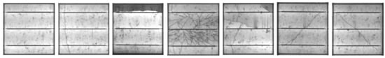
Figure 5. Classification of crack directions. Types of cracks from left to right: No crack, perpendicular crack, parallel crack, dendritic crack, multiple directional cracks, +45∘ cracks and −45∘ cracks (Reprinted from Renewable Energy, Vol 145, Lamprini Papargyri, Marios Theristis, Bernhard Kubicek, Thomas Krametz, Christoph Mayr, Panos Papanastasiou, George Georghiou, Modelling and experimental investigations of microcracks in crystalline silicon photovoltaics: A review, 2387–2408, Copyright (2021), with permission from Elsevier) [17].
Regarding the severity of the microcracks, Kontges et al. [13], classified microcracks into three different categories: Mode A, B, and C, as shown in Figure 6. Mode A fissures do not represent a significant power loss [13], as they do not generate inactive areas on the cell (electrically disconnected pieces), although they are a weak point on the cell and can eventually evolve to more severe cracks such as modes B and C when exposed to outdoor conditions with heat, wind, or snow [19].

Figure 6. Electroluminescence microcrack modes A, B, and C (Reprinted from Solar Energy Materials and Solar Cells, Vol 95, issue 4, Kntges, M., Kunze, I., Kajari-Schrder, S., Breitenmoser, X., Bjørneklett, B., The risk of power loss in crystalline silicon based photovoltaic modules due to micro-cracks, 1131–1137, Copyright (2021), with permission from Elsevier) [13].
The power loss caused by microcracks becomes significantly bigger when parts of the solar cell disconnect electrically from the rest of the cell, as the generation of a PV solar cell is directly proportional to the active area. Therefore, microcracks become a serious issue when portions of the cell become electrically isolated. This means that there will be areas with no current collected from the fingers to the bus bar of the cell. An inactive area of 50% or higher can lead to a power loss of one-third of the module’s power. This happens due to the activation of the module bypass diode, which shortcuts the portion of the PV module with a significant crack [20], as seen in Figure 7.

Figure 7. Bypassed cells due to cracks.
The effect of microcracks on C-Si cells can be seen in Figure 8. The presence of micro fissures on the cells can cause a reduction of the short circuit current and shunt resistance. When the cracking of the cells is not uniform throughout the module, the I-V curve is commonly stepped [21].
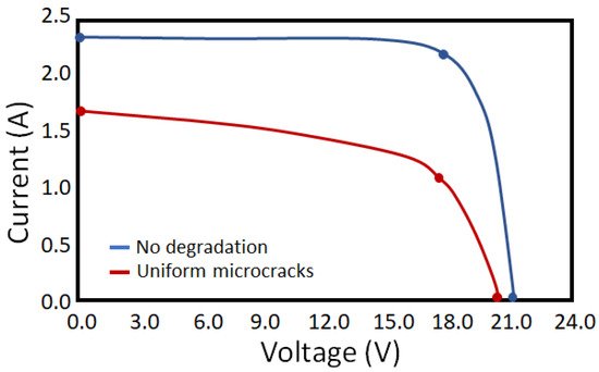
Figure 8. Microcracks degradation effect on I-V curve [21].
Strategies to overcome and reduce the occurrence of microcracks on the solar cell have been studied at the cell, module, and system levels. At the cell level, a common crack that occurs is when part of the effective area of the cell is lost as the crack occurs beyond the outer busbars and the edge of the solar cell. The current from the detached portion of the cell can not be collected by the busbars. On the other hand, when the crack is located between two busbars, the redundancy of the busbars allow the current from the cracked region to still be collected although an increase in the resistive losses in the fingers is expected. Therefore, an alternative to reduce the effects of power loss caused by microcracks is to increase the number of busbars and re-position the outer busbars closer to the cells edge [19]. At the module level, despite the soldering strategies to reduce the damage on the semiconductor, construction strategies such as glass-glass modules can be used to reduce the propagation of microcracks. With this technology the cell is positioned in a neutral point, and less likely to suffer tensile stress. At system level, maximum power point tracking (MPPT) strategies, the use of microinverters and charge controllers can help overcome the losses caused by under performing modules [17][19]
3. Potential Induced Degradation
The potential-induced degradation (PID) effect has been considered the most frequent problem in crystalline silicon cells [22][23]. This phenomenon originates from the movement of static electrical charge (leakage current) between the solar cell and the grounded structure of the module due to a large potential difference [24]. This failure can cause a substantial and rapid loss normally up to 30% of the initial power which leads to a considerable financial impact [23][24]. Studies have shown that PID can affect both p-type and n-type cells, although heterojunction cells seem to be more resilient to this degradation due to the conductive transparent conducting oxide layer [24].
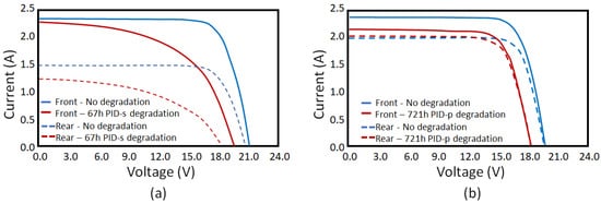
The difference of the electric potential between the solar cell and the module’s frame in p-type solar cells can cause the migration of sodium ions (Na+). These Na+ ions diffuse into stacking faults of the silicon lattice, reaching the semiconductor pn-junction. Consequently, direct metallic shunt paths are created, which reduces the cell’s shunt resistance. This reduction of the shunt resistance directly affects the fill factor (FF) of the I-V curve. In cases where the degradation level is up to 40%, the short-circuit current and open-circuit voltage are not affected. Although, any degradation above this value will make the short-circuit current and open-circuit voltage drop drastically [23]. This degradation was defined by Neymann et al. [25] as “PID of the shunting type” (PID-s). Another PID found in p-passivated emitter and rear cell (PERC) solar cells is the “PID of the polarisation type” (PID-p). This type of PID can increase the surface recombination by deteriorating the normal functioning of the passivation layer. This deterioration occurs due to the negative charge present in the AlOx present in the rear side passivation layer is canceled by the positive charges present in the Na+ ions [26][27]. This type of degradation can drop Isc and Voc significantly, but the decrease in FF is small [28]. Figure 9 shows the effect of PID-s and PID-p on the front and rear side I-V curves of BPV cells.
To generate energy from both sides of the module, bifacial cells have the rear side only partially covered with metal contacts. Although it allows a photocurrent to be generated from the irradiance incident on the rear side, it affects the electromagnetic shielding of of the passivating AlOx, SiNy layers and the bulk Si [30]. As a consequence, bifacial PV cells are more vulnerable to PID. Bifacial p-PERC cells affected by bifacial PID suffer from shunting of the pn-junction (PID of the shunt type - PID-s) and an increase in the surface recombination at the rear side (PID of the polarised type - PID-p) [23]. BPV modules with double glass and EVA encapsulant are more susceptible to PID as there is an increase in the availability of Na+ ions from the glass. The use of polyolefin encapsulants can prevent or reduce the occurrence of PID [31]. Additionally, studies have shown that the rear side of the bifacial cell is more affected by PID than the front side in both degradation level and degradation rate [22][23].
Both PID-s and PID-p can be reversible. To revert the degradation effects, the cell can be placed under a positive bias compared to the grounded frame or by increasing the module’s temperature, which is not easily feasible in outdoor conditions. Another solution to revert the PID-p effect on p-PERC cells is by exposing the module to light [22][23][28]. Additionally, PID can be prevented at different stages. At the cell level, increasing the refractive index of the anti-reflective coat can reduce the susceptibility of PID to occur [32][33][34]. For modules, different materials known as “PID resistant” or “PID-free” can be used as encapsulants, or materials such as borosilicate glass can be used in the fabrication process to protect the module against the PID effect. At a system level, the ground can be modified/configured to make the electrical field repel the Na+ ions move away from the solar cells [23][32].
4. Light Induced Degradation
The defects caused by classical impurities are widely explored and understood, on the other hand, degradation such as light-induced degradation (LID) and light and temperature-induced degradation (LeTID) still need attention and further studies especially with the improvement of the cell structure using surface passivation layers [35]. These degradations have shown to be more significant in the PERC technology. PERC technology improved the efficiency of the existing solar cells, enabling efficiency levels of 21–24% without a significant increase in price [36]. In PERC p-type multi-crystalline silicon cells, the effect of LID can cause a reduction in the power output of the module at the maximum power point (MPP) by around 10% [37][38]. This Light Induced Degradation (LID) is caused by the natural exposition of the PV modules to solar irradiance and an excess of carrier injection by above-bandgap illumination or forward biasing [39]. In the I-V characteristics of the solar cell or module, LID can be seen as a reduction of the short-circuit current and open-circuit voltage as shown in Figure 10. This behaviour in the I-V characteristic curve is due to the increase in minority-carrier recombination in the bulk of the c-Si [39]. Despite the extensive studies regarding LID, the actual recombination-active defects which are responsible for causing the degradation, are still not identified.

Figure 10. I-V curve of simulated PV module with LID [40].
The boron-oxygen molecules are generated due to the exposition of the cell to sunlight. This effect occurs during the first few hours of light exposure at ambient temperature and is detected by the monitoring of the system performance for the first week after installation [24]. These boron-oxygen molecules can absorb the photo-generated electron-hole pair, which leads to a reduction of the cell’s short-circuit current and maximum power [24]. BO-LID can be permanently deactivated by simultaneous illumination and annealing using one sun irradiance intensity at temperature levels of 60–300 ∘C [41]. This method can dissociate the B-O complex [42], although, as the temperature required for the reversion process is considerably high, it is unachievable in the field. Therefore, it makes the failure hard to recover for modules in operation. For this reason, to prevent this degradation, the manufacturer must perform preliminary light soaking tests on the cells/modules for the correct standard qualification according to the IEC 61215.
Another type of LID is related to the dissociation of iron-boron (FeB-LID) pairs and is more common in multi-crystalline silicon cells (mc-Si) [43]. Under dark condition, the positively charged atoms of iron associate with the negatively charged boron atoms. These Fe-B complexes that are formed do not affect cell efficiency and have very narrow energy levels. On the other hand, under illumination, there will be a shift in the Fermi level. This shift caused the neutralisation of the iron ions and the separation of the iron atoms from the boron atoms. The free iron atoms cause higher carrier recombination while the cell is exposed to sunlight. Therefore, the dissociation of the Fe-B pairs causes an efficiency loss, especially in cells with high iron contamination during the first few minutes of light exposure [40]. More research and a better understanding of both LID and LeTID are of extreme importance in order to potentially reduce the degradation effects caused by light or light and temperature-induced degradation, which increase the losses and the uncertainties regarding the performance of the system in the field.
5. Light and Elevate Temperature Induced Degradation
Another degradation effect caused by the exposure of the cell to light, is the Light and elevate Temperature Degradation (LeTID). This degradation was first discovered in 2012 [44] and it causes loss in module performance when the cells are exposed to both light and elevated temperature (>50 ∘C) for a long period. It has been reported that LeTID does not occur if the module operates at a temperature below 50 ∘C or if it operates above this temperature for a short period [24]. This degradation has been reported to appear if the manufacturing process of the solar cell involves a high-temperature exposure followed by an abrupt cooling [24]. Similarly to LID, LeTID affects solar cells dielectrically passivated on the rear side (PERC) more significantly than aluminium back surface field (Al-BSF) cells [45]. Although no method of detection and prevention has been agreed to date, studies have shown that LeTID happens at a much slower degradation rate than what has been experienced with LID [24]. It can take years of exposure to sunlight and elevate temperature until the cell start showing sings of LeTID.
The origin of LeTID is still unknown, although numerous studies have suggested a relation between high concentration of weakly bonded hydrogen in the region near the passivation layers of the cell as a cause of LeTID [37][46][47]. The hydrogen is released from the hydrogen rich SiNx:H (Hydrogen-Rich Silicon Nitride) layer during the rapid thermal annealing (RTA) and its amount varies with the thickness and composition of the layer [48][49]. Under illumination and high temperature exposure for a long period, hydrogen atoms can bond to silicon atoms, which can give rise to a slow degradation of the maximum power which can reach values up to 7% [24]. This degradation caused by LeTID can be reversed naturally but sometimes not completely. The reversion process happens when the cell is exposed to the same high-temperature condition that causes the degradation for some time [24]. The occurrence of LeTID is independent of the dopant used in the cell, therefore it can affect both p-type or n-type silicon cells [46]. This degradation can take many years to recover in systems installed in field, which causes a significant loss in the energy yield over time [50].
At modules level, when exposed to 40 kWh/m2, both monofacial and bifacial PV modules had the same relative degradation of 1.3%. As the solar radiation levels increases to 100 kWh/m2, bifacial PV modules degradation only increase 0.1% while monofacial increased 0.6%. More research on the effects of LeTID in bifacial PV modules is needed, although, based on [51] it can be expected that the LeTID effects on bifacial modules will be less significant.
The LeTID recovery process requires the exposure of the cell to high temperature treatments. The higher the temperature, the cell is exposed to in the recovery process, the faster is the recovery process. However, it was found that high temperature recoveries can lead to an incomplete recovery of LeTID. Studies are still being performed to identify the threshold between time, temperature, and LeTID recovery [43].
6. Soiling
Also known as natural dust effect, it is caused by airborne particles of dust that deposit on the external parts of a PV module over a period of time. These particles vary on type and size from 1 μm to 500 μm [52]. Although soiling of the module is not standardized as a PV module failure[20], it significantly impacts the performance of a PV system by partially shading it. The dust particles can act as dielectrics by absorbing the irradiance, or by changing the angle of incidence of the irradiance on the surface of the module. Both issues result in the decrease of the total irradiance reaching the module’s surface [52]. For monofacial modules, it has been shown that the soiling degradation can reduce the power output from 2% to 60%. This variation depends on the time, the area with the particles accumulation, and the cleaning strategies [53]. The soiling effect becomes a higher threat in locations with high relative humidity, which may increase the stickiness of the soil particles. As a result, the cleaning capacity of wind and rain will be reduced [54]. The intensity of soiling varies for each specific location.
The solution to minimize the degradation effects caused by soiling is the application of strategic cleaning routines [55]. However, cleaning strategies are not the only solution to overcome soiling. Researchers have identified methods to remove the dust accumulated on the surface of the module by using electrodynamics screens (EDS), super hydrophobic plane (SHOP), and super hydrophilic plane (SHIP). In the EDS method, electrodes are positioned on the solar module and provide a self-cleaning strategy by the generation of an electric field. This method presents a 90% efficiency in less than 2 min cleaning and utilizes less than 0.1% of the energy generated by the collectors [56]. SHOP and SHIP strategies have the benefit of being passive cleaning methods, which means that there is no requirement of power input. The SHOP method uses a hydrophobic coat. This method shows high efficiency at cleaning under raining weather, although it is considered inefficient for dry dust [57]. The SHIP method uses a nano-film of titanium oxide, chemical coating, and nano-patterned fabrication of glass surface to create a super hydrophilic surface. This method has the benefits included in SHOP and it can chemically break down the organic particles of dust through a reaction with the UV light in a photocatalytic process [57]. It is more durable than SHOP. However, it acts as a dust suspender, therefore regular washings are still required to wash off the dust, especially in dry climates [57][58].
For bifacial, the cleaning process of the rear side is not as straight forward. Luque et al. [59], performed an analysis comparing the degradation rate between MPV and BPV modules in Chile by measuring the short-circuit current. It was found that the degradation rate from soiling is much lower for BPV technology (approximately 21.6%). The average soiling degradation rate for MPV was 0.301% whilst BPV was 0.236% on the front side. It was observed that soiling does not have much impact on the rear side, showing an average of 0.039%, nearly 85% lower than the front side. Bhaduri et al. [60] compared the effects of soiling in MPV and BPV mounted at a latitude tilt angle and vertically in Mumbai. The results showed that vertically mounted BPV modules are more resilient to soiling effects compared to vertical MPV modules and tilted MPV and BPV modules. The gain obtained from the vertically installed BPV module surpassed the tilted BPV after three weeks without cleaning. The soiling degradation rate for MPV and BPV modules mounted at a tilt are similar. For monofacial the average soiling loss rate per day was 0.40% whilst bifacial is 0.39%. On the other hand the degradation rate for BPV modules installed vertically was 0.02% per day.
This entry is adapted from the peer-reviewed paper 10.3390/en14237935
References
- VDMA. International Technology Roadmap for Photovoltaic, 11th ed.; ITRPV: Frankfurt am Main, Germany, 2020; p. 76.
- King, D.L.; Quintana, M.A.; Kratochvil, J.A.; Ellibee, D.E.; Hansen, B.R. Photovoltaic module performance and durability following long-term field exposure. AIP Conf. Proc. 2009, 462, 565–571.
- Mohan, B.V.G.; Mayandi, J.; Pearce, J.M.; Muniasamy, K.; Veerapandy, V. Demonstration of a simple encapsulation technique for prototype silicon solar cells. Mater. Lett. 2020, 274, 128028.
- Sinha, A.; Sastry, O.S.; Gupta, R. Nondestructive characterization of encapsulant discoloration effects in crystalline-silicon PV modules. Sol. Energy Mater. Sol. Cells 2016, 155, 234–242.
- Oreski, G.; Wallner, G.M. Evaluation of the aging behavior of ethylene copolymer films for solar applications under accelerated weathering conditions. Sol. Energy 2009, 83, 1040–1047.
- Kim, C.; Jeong, M.S.; Ko, J.; Ko, M.G.; Kang, M.G.; Song, H.J. Inhomogeneous rear reflector induced hot-spot risk and power loss in building-integrated bifacial c-Si photovoltaic modules. Renew. Energy 2021, 163, 825–835.
- Chattopadhyay, S.; Dubey, R.; Kuthanazhi, V.; John, J.J.; Solanki, C.S.; Kottantharayil, A.; Arora, B.M.; Narasimhan, K.L.; Kuber, V.; Vasi, J.; et al. Visual degradation in field-aged crystalline silicon PV modules in India and correlation with electrical degradation. IEEE J. Photovol. 2014, 4, 1470–1476.
- Sinha, A.; Hurst, K.; Ulicna, S.; Schelhas, L.T.; Miller, D.C.; Hacke, P. Assessing UV-Induced Degradation in Bifacial Modules of Different Cell Technologies. In Proceedings of the 48th Photovoltaic Specialists Conference (PVSC), Fort Lauderdale, FL, USA, 20–25 June 2021; pp. 0767–0770.
- Albadwawi, O.; Alhamadani, H.; Hassan, S.; John, J.J.; Alheloo, A.; Almheiri, A.; Alnuaimi, A. Investigation of Bifacial PV modules degradation under desert climatic conditions. In Proceedings of the 47th IEEE Photovoltaic Specialists Conference (PVSC), Calgary, AB, Canada, 15 June–21 August 2020; pp. 1505–1509.
- Sinha, A.; Sulas-Kern, D.; Owen-Bellini2, M.; Spinella, L.; Ulicna, S.; Ayala Pelaez, S.; Johnston, S.; Schelhas, L. Glass/Glass Photovoltaic Module Reliability and Degradation: A Review Manuscript version: Accepted Manuscript. J. Phys. D Appl. Phys. 2021, 41, 413002.
- Realini, A.; Cereghetti, N.; Chianese, D. Mean Time Before Failure of Photovoltaic Modules; Swiss Federal Office of Energy: Canobbio, Switzerland, 2002.
- Camino, B. Designing New Materials for Photocathodes. Ph.D. Thesis, Department of Chemistry, Imperial College London, London, UK, 2017.
- Köntges, M.; Kunze, I.; Kajari-Schröder, S.; Breitenmoser, X.; Bjørneklett, B. The risk of power loss in crystalline silicon based photovoltaic modules due to micro-cracks. Sol. Energy Mater. Sol. Cells 2011, 95, 1131–1137.
- Spataru, S.; Hacke, P.; Sera, D. Automatic Detection and Evaluation of Solar Cell Micro-Cracks in Electroluminescence Images Using Matched Filters. In Proceedings of the 2016 IEEE 43rd Photovoltaic Specialists Conference (PVSC), Portland, OR, USA, 5–10 June 2016; pp. 1602–1607.
- Bdour, M.; Dalala, Z.; Al-Addous, M.; Radaideh, A.; Al-Sadi, A. A Comprehensive Evaluation on Types of Microcracks and Possible Effects on Power Degradation in Photovoltaic Solar Panels. Sustainability 2020, 12, 6416.
- Ennemri, A.; Logerais, P.O.; Balistrou, M.; Durastanti, J.F.; Belaidi, I. Cracks in silicon photovoltaic modules: A review. J. Optoelectron. Adv. Mater. 2019, 21, 74–92.
- Papargyri, L.; Theristis, M.; Kubicek, B.; Krametz, T.; Mayr, C.; Papanastasiou, P.; Georghiou, G.E. Modelling and experimental investigations of microcracks in crystalline silicon photovoltaics: A review. Renew. Energy 2019, 145, 2387–2408.
- Wen, T.K.; Yin, C.C. Crack detection in photovoltaic cells by interferometric analysis of electronic speckle patterns. Sol. Energy Mater. Sol. Cells 2012, 98, 216–223.
- Gabor, A.M.; Janoch, R.; Anselmo, A.; Field, H. Solar Panel Design Factors to Reduce the Impact of Cracked Cells and the Tendency for Crack Propagation; NREL PV Module Reliability Workshop: Denver, CO, USA, 2015; pp. 1–11.
- Köntges, M.; Kurtz, S.; Packard, C.; Jahn, U.; Berger, K.; Kato, K.; Friesen, T.; Liu, H.; Van Iseghem, M. Review of Failures of Photovoltaic Modules; Photovoltaic Power Systems Programme; International Energy Agency: Paris, France, 2014; pp. 1–140.
- Ahmad, J.; Ciocia, A.; Fichera, S.; Murtaza, A.F.; Spertino, F. Detection of typical defects in silicon photovoltaic modules and application for plants with distributed MPPT configuration. Energies 2019, 12, 4547.
- Luo, W.; Khoo, Y.S.; Hacke, P.; Naumann, V.; Lausch, D.; Harvey, S.P.; Singh, J.P.; Chai, J.; Wang, Y.; Aberle, A.G.; et al. Potential-induced degradation in photovoltaic modules: A critical review. Energy Environ. Sci. 2017, 10, 43–68.
- Carolus, J.; Tsanakas, J.A.; van der Heide, A.; Voroshazi, E.; De Ceuninck, W.; Daenen, M. Physics of potential-induced degradation in bifacial p-PERC solar cells. Sol. Energy Mater. Sol. Cells 2019, 200, 109950.
- Pravettoni, M. Module Deployment and Energy Rating; Springer International Publishing: Berlin/Heidelberg, Germany, 2020; Volume 301, pp. 249–283.
- Naumann, V.; Lausch, D.; Hähnel, A.; Bauer, J.; Breitenstein, O.; Graff, A.; Werner, M.; Swatek, S.; Großer, S.; Bagdahn, J.; et al. Explanation of potential-induced degradation of the shunting type by Na decoration of stacking faults in Si solar cells. Sol. Energy Mater. Sol. Cells 2014, 120, 383–389.
- Halm, A.; Schneider, A.; Mihailetchi, V.D.; Koduvelikulathu, L.J.; Popescu, L.M.; Galbiati, G.; Chu, H.; Kopecek, R. Potential-induced Degradation for Encapsulated n-type IBC Solar Cells with Front Floating Emitter. Energy Procedia 2015, 77, 356–363.
- Green, M.A. The Passivated Emitter and Rear Cell (PERC): From conception to mass production. Sol. Energy Mater. Sol. Cells 2015, 143, 190–197.
- Luo, W.; Hacke, P.; Terwilliger, K.; Liang, T.S.; Wang, Y.; Ramakrishna, S.; Aberle, A.G.; Khoo, Y.S. Elucidating potential-induced degradation in bifacial PERC silicon photovoltaic modules. Prog. Photovolt. Res. Appl. 2018, 26, 859–867.
- Carolus, J.; Breugelmans, R.; Tsanakas, J.A.; van der Heide, A.; Voroshazi, E.; De Ceuninck, W.; Daenen, M. Why and how to adapt PID testing for bifacial PV modules? Prog. Photovolt. Res. Appl. 2020, 28, 1045–1053.
- Sporleder, K.; Turek, M.; Schüler, N.; Naumann, V.; Hevisov, D.; Pöblau, C.; Großer, S.; Schulte-Huxel, H.; Bauer, J.; Hagendorf, C. Quick test for reversible and irreversible PID of bifacial PERC solar cells. Sol. Energy Mater. Sol. Cells 2021, 219, 110755.
- Stein, J.S.; Reise, C.; Castro, J.B.; Friesen, G.; Maugeri, G.; Urrejola, E.; Ranta, S. Bifacial PV modules and systems Experience and Results from International Research and Pilot Applications. Report IEA-PVPS T13-14:2021; Photovoltaic Power Systems Programme; International Energy Agency: Paris, France, 2021; pp. 1–168.
- Pingel, S.; Frank, O.; Winkler, M.; Oaryan, S.; Geipel, T.; Hoehne, H.; Berghold, J. Potential induced degradation of solar cells and panels. In Proceedings of the 35th IEEE Photovoltaic Specialists Conference, Honolulu, HI, USA, 20–25 June 2010; pp. 2817–2822.
- Koch, S.; Nieschalk, D.; Berghold, J.; Wendlandt, S.; Krauter, S.; Grunow, P. Potential induced degradation effects on crystalline silicon cells with various antireflective coatings. In Proceedings of the 27th European Photovoltaic Solar Energy Conference and Exhibition, Frankfurt, Germany, 24–28 September 2012; pp. 1985–1990.
- Janssen, G.J.; Stodolny, M.K.; Van Aken, B.B.; Loffler, J.; Lamers, M.W.; Tool, K.J.; Romijn, I.G. Minimizing the Polarization-Type Potential-Induced Degradation in PV Modules by Modification of the Dielectric Antireflection and Passivation Stack. IEEE J. Photovol. 2019, 9, 608–614.
- Wilson, G.M.; Al-Jassim, M.; Metzger, W.K.; Glunz, S.W.; Verlinden, P.; Xiong, G.; Mansfield, L.M.; Stanbery, B.J.; Zhu, K.; Yan, Y.; et al. The 2020 photovoltaic technologies roadmap. J. Phys. D Appl. Phys. 2020, 53, 493001.
- Lin, D.; Hu, Z.; He, Q.; Yang, D.; Song, L.; Yu, X. New insights on LeTID/BO-LID in p-type mono-crystalline silicon. Sol. Energy Mater. Sol. Cells 2021, 226, 111085.
- Nakayashiki, K.; Hofstetter, J.; Morishige, A.E.; Li, T.T.A.; Needleman, D.B.; Jensen, M.A.; Buonassisi, T. Engineering Solutions and Root-Cause Analysis for Light-Induced Degradation in p-Type Multicrystalline Silicon PERC Modules. IEEE J. Photovol. 2016, 6, 860–868.
- Kraus, K.; Brand, A.A.; Fertig, F.; Rein, S.; Nekarda, J. Fast regeneration processes to avoid light-induced degradation in multicrystalline silicon solar cells. In Proceedings of the 2017 IEEE 44th Photovoltaic Specialist Conference, PVSC 2017, Washington, DC, USA, 25–30 June 2017; Volume 6, pp. 1–3.
- Lindroos, J.; Savin, H. Review of light-induced degradation in crystalline silicon solar cells. Sol. Energy Mater. Sol. Cells 2016, 147, 115–126.
- Luka, T.; Hagendorf, C.; Turek, M. Multicrystalline PERC solar cells: Is light-induced degradation challenging the efficiency gain of rear passivation? Photovolt. Int. 2016, 32, 37–44.
- Herguth, A.; Schubert, G.; Kaes, M.; Hahn, G. Investigations on the long time behavious of the metastable Boron-Oxygen complex in crystalline silicon. IEEE Trans. Fuzzy Syst. 2007, 20, 1114–1129.
- Sopori, B.; Basnyat, P.; Devayajanam, S.; Shet, S.; Mehta, V.; Binns, J.; Appel, J. Understanding light-induced degradation of c-Si solar cells. In Proceedings of the IEEE Photovoltaic Specialists Conference, Austin, TX, USA, 3–8 June 2012; pp. 1115–1120.
- Herguth, A.; Derricks, C.; Keller, P.; Terheiden, B. Recovery of LeTID by low intensity illumination: Reaction kinetics, completeness and threshold temperature. Energy Procedia 2017, 124, 740–744.
- Ramspeck, K.; Zimmermann, S.; Nagel, H.; Metz, A.; Gassenbauer, Y.; Birkmann, B.; Seidl, A. Light Induced Degradation of Rear Passivated mc-Si Solar Cells. In Proceedings of the 27th European Photovoltaic Solar Energy Conference and Exhibition, Frankfurt, Germany, 24–28 September 2012; pp. 861–865.
- Kersten, F.; Fertig, F.; Petter, K.; Klöter, B.; Herzog, E.; Strobel, M.; Heitmann, J.; Müller, J. Performance Loss Induced by LeTID in the Field. In Proceedings of the 33rd European Photovoltaic Solar Energy Conference, Amsterdam, The Netherlands, 25–29 September 2017; pp. 1418–1421.
- Chen, D.; Hamer, P.; Kim, M.; Chan, C.; Ciesla nee Wenham, A.; Rougieux, F.; Zhang, Y.; Abbott, M.; Hallam, B. Hydrogen-induced degradation: Explaining the mechanism behind light- and elevated temperature-induced degradation in n- and p-type silicon. Sol. Energy Mater. Sol. Cells 2020, 207, 110353.
- Inglese, A.; Focareta, A.; Schindler, F.; Schön, J.; Lindroos, J.; Schubert, M.C.; Savin, H. Light-induced Degradation in Multicrystalline Silicon: The Role of Copper. Energy Procedia 2016, 92, 808–814.
- Zhang, Y.; Yu, Y.; Meng, F.; Liu, Z. Experimental Investigation of the Shading and Mismatch Effects on the Performance of Bifacial Photovoltaic Modules. IEEE J. Photovol. 2020, 10, 296–305.
- Bredemeier, D.; Walter, D.C.; Heller, R.; Schmidt, J. Impact of Hydrogen-Rich Silicon Nitride Material Properties on Light-Induced Lifetime Degradation in Multicrystalline Silicon. Phys. Status Solidi Rapid Res. Lett. 2019, 13, 1–5.
- Jensen, M.A.; Zuschlag, A.; Wieghold, S.; Skorka, D.; Morishige, A.E.; Hahn, G.; Buonassisi, T. Evaluating root cause: The distinct roles of hydrogen and firing in activating light-and elevated temperature-induced degradation. J. Appl. Phys. 2018, 124, 085701.
- Zhang, D.; Wu, J. Comparison of Letid in Monofacial and Bifacial Multicrystalline PERC cells and modules. In Proceedings of the 37th European Photovoltaic Solar Energy Conference and Exhibition, Lisbon, Portugal, 7–11 September 2020.
- Urrejola, E.; Antonanzas, J.; Ayala, P.; Salgado, M.; Ramírez-Sagner, G.; Cortés, C.; Pino, A.; Escobar, R. Effect of soiling and sunlight exposure on the performance ratio of photovoltaic technologies in Santiago, Chile. Energy Convers. Manag. 2016, 114, 338–347.
- Hoffman, A.R.; Maag, C.R. Photovoltaic Module Soiling Studies May 1978–October 1980; May 1978–October 1980 DOE/JPL-1012-49; Jet Propulsion Laboratory: La Cañada Flintridge, CA, USA, 1980.
- Guo, B.; Javed, W.; Figgis, B.W.; Mirza, T. Effect of dust and weather conditions on photovoltaic performance in Doha, Qatar. In Proceedings of the 2015 1st Workshop on Smart Grid and Renewable Energy, SGRE 2015, Doha, Qatar, 22–23 March 2015.
- Maghami, M.R.; Hizam, H.; Gomes, C.; Radzi, M.A.; Rezadad, M.I.; Hajighorbani, S. Power loss due to soiling on solar panel: A review. Renew. Sustain. Energy Rev. 2016, 59, 1307–1316.
- Mazumder, M.; Horenstein, M.N.; Stark, J.W.; Girouard, P.; Sumner, R.; Henderson, B.; Sadder, O.; Hidetaka, I.; Biris, A.S.; Sharma, R. Characterization of electrodynamic screen performance for dust removal from solar panels and solar hydrogen generators. IEEE Trans. Ind. Appl. 2013, 49, 1793–1800.
- Deb, D.; Brahmbhatt, N.L. Review of yield increase of solar panels through soiling prevention, and a proposed water-free automated cleaning solution. Renew. Sustain. Energy Rev. 2018, 82, 3306–3313.
- He, G.; Zhou, C.; Li, Z. Review of self-cleaning method for solar cell array. Procedia Eng. 2011, 16, 640–645.
- Luque, E.G.; Antonanzas-Torres, F.; Escobar, R. Effect of soiling in bifacial PV modules and cleaning schedule optimization. Energy Convers. Manag. 2018, 174, 615–625.
- Bhaduri, S.; Kottantharayil, A. Mitigation of Soiling by Vertical Mounting of Bifacial Modules. IEEE J. Photovol. 2019, 9, 240–244.
This entry is offline, you can click here to edit this entry!