Silicon photonics has drawn increasing attention since recent decades and is promising to act as a key technology for future daily applications due to its various merits including ultra-low cost, high integration density owing to the high refractive index of silicon and compatibility with current semiconductor fabrication process. Optical interconnects is an important issue in silicon photonic integrated circuits to transmit light and fiber-to-chip optical interconnects is vital in application scenarios like data centers and optical transmission systems. There are mainly two categories of fiber-to-chip optical coupling, that is off-plane coupling and in-plane coupling. Grating couplers work under the former category while edge couplers function as in-plane coupling. In this paper, we mainly focus on edge couplers in silicon photonic integrated circuits. We deliver an introduction to the research background, operation mechanism and design principles of silicon photonic edge couplers. The state-of-the-art of edge couplers is reviewed according to different configurations as to the device structure, identifying the performance, fabrication feasibility and applications. In addition, a brief comparison between edge couplers and grating couplers is conducted. Packaging issue is also discussed and several prospective techniques for further improvements of edge couplers are proposed.
- silicon photonics
- optical interconnects
- fiber-to-chip coupling
- edge couplers
- inverse taper
1. Definition
Silicon photonics has drawn increasing attention in the past few decades and is a promising key technology for future daily applications due to its various merits including ultra-low cost, high integration density owing to the high refractive index of silicon, and compatibility with current semiconductor fabrication process. Optical interconnects is an important issue in silicon photonic integrated circuits for transmitting light, and fiber-to-chip optical interconnects is vital in application scenarios such as data centers and optical transmission systems. There are mainly two categories of fiber-to-chip optical coupling: off-plane coupling and in-plane coupling. Grating couplers work under the former category, while edge couplers function as in-plane coupling.
2. Introduction
As the size of electronic integrated circuits scales down to the physical limit and the demand for high data rates rises tremendously, photonic integrated circuits (PIC) has gradually taken the stage due to its inherent high speed and low power consumption. Silicon has the potential to construct compact devices benefiting from its high refractive index, and silicon-based devices are well compatible with current mature and standardized complementary metal oxide semiconductor (CMOS) platform. Thus, silicon is a promising material for novel PIC, and silicon photonics has been a hot research topic in recent years [1][2][3][4][5]. In cases of complex optical transmission systems, optical interconnects between fiber and the photonic integrated circuits happen frequently in the whole system [6], so efficient fiber-to-chip coupling is an important factor to pay attention to for system performance [7][8][9][10]. To date, the feature size of silicon waveguide can be as tiny as tens of nanometers while the typical diameter of a single mode fiber (SMF) is around 125 μm with a core diameter near 10 μm [11]. Figure 1 shows the huge size mismatch between a fiber core and the Si waveguide, which causes considerable optical transmission loss when light emitting from the fiber core enters the Si waveguide directly. Fiber-to-chip couplers are a type of key photonic component to deal with this issue in optical interconnects.
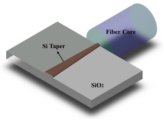
Figure 1. Schematic of optical interconnects between fiber and photonic chip.
Fiber-to-chip couplers can be applied in many application scenarios where optical interconnects are required. They are passive devices that can transmit and guide light. The operation mechanism is mainly the transmission and conversion of mode in the photonic waveguides. Generally, there are two main approaches of fiber-to-chip coupling, namely vertical coupling (or off-plane coupling) and butt coupling (or edge coupling/in-plane coupling) [12][13], according to the relative position of fiber and the photonic chip. For vertical coupling, grating couplers are mostly used, and fiber is placed above the device vertically or slightly slanted at a certain degree to ensure high coupling efficiency [14][15][16][17][18][19][20][21][22][23]. Grating couplers have some major advantages including compact size, wafer-level testing capability, and flexible coupling position, while there are also some drawbacks such as a relatively low coupling efficiency typically below 3 dB, narrow bandwidth, and high wavelength sensitivity. As for the butt coupling regime, under which the fiber is typically placed at the wafer facet and aligned with the Si waveguides horizontally, edge couplers are commonly applied [24][25][26][27][28][29][30][31][32]. Edge couplers can achieve rather high coupling efficiency, broad bandwidth, and polarization independence, but they also have some limitations including relatively a larger footprint than grating couplers, fixed coupling position, and more strict requirements of the coupling facet.
3. Data, Model, Applications and Influences
3.1. Operation Mechanism and Design Principles of Edge Couplers
Fiber-to-chip edge couplers have been widely investigated by researchers for decades, and the inverse taper structure plays an indispensable role in edge coupling [33]. Corresponding to the direction of light propagation, inverse taper refers to a tapering waveguide with a gradual increase in width along the mode propagation direction, which means the narrow end of the taper is close to fiber, while the wide end is connected with photonic waveguides. Modal distribution is determined by both the mode order and the waveguide structure. For a specific mode, only waveguides with a certain cross-section area can support the entire mode [34]. The fundamental transverse electric (TE) mode is mostly applied in optical communication applications to transmit information, and most of the researches on silicon photonic edge couplers studied the transverse electric mode. The most commonly used size of silicon photonic waveguide that can support the fundamental TE mode propagation at negligible loss is about 200 nanometers high and about 500 nanometers wide [35]. A waveguide with a too small cross-section area cannot support an entire fundamental mode, and thus the mode will partially distribute in the outer region of the waveguide. In contrast, a waveguide with a too large cross-section area will easily excite undesirable higher-order modes [36][37][38]. The taper is just appropriate for mode conversion, since a gradually varying cross-section area supports mode transformation and mode size variation. On this basis, the narrow end of the inverse taper has a smaller cross-section area than the expected modal size, so it is unable to confine the incident mode completely, and a considerable percentage of the electromagnetic field distributes surrounding the taper tip. As the taper width becomes larger, it can support the entire mode and confine the electromagnetic field inside the taper integrally. Overall, an edge coupler based on an inverse taper whose narrow tip is aligned to the fiber core can convert a large mode incident from the optical fiber to the compressed guided mode in photonic waveguides.
When evaluating the performance of an edge coupler, there are some general metric parameters including coupling efficiency (or coupling loss), device footprint, operating bandwidth, fabrication deviation tolerance, and misalignment tolerance [39]. Coupling efficiency is the most critical and fundamental parameter for an edge coupler, indicating the ratio of output power over the input power after light transmission and mode conversion inside the edge coupler. To achieve a high coupling efficiency is the main goal in designing optical couplers. The device footprint is another important parameter to define the advantage of an edge coupler considering the integration density, fabrication feasibility, and packing difficulty. Photonic devices with a compact size are desired for improving the integration density and reducing the cost. Since edge couplers generally consist of tapers that are longitudinal shaped, the main idea of achieving a compact edge coupler is to decrease the device length. When it comes to wavelength characteristics, an edge coupler has the inherent advantage of broad operating bandwidth, since it works based on the propagation property of light rather than the diffraction effect of light in grating couplers. The broad operating bandwidth implies that the edge coupler can work efficiently and stably in a wide wavelength range, insensitive to wavelength fluctuation. In addition, due to the structural symmetry and simplicity, edge couplers based on a single taper are easy and straightforward to fabricate and have good fabrication deviation tolerance and misalignment tolerance.
3.2. Structural Transformations of Edge Couplers in Horizontal Direction
An edge coupler based on one standard single inverse taper is the most basic and straightforward formation for all various types of edge couplers. When the thickness of the Si waveguide is constant while the width decreases gradually toward the fiber, the Si strip waveguide becomes a taper. Light cannot be confined properly within the narrow taper end. Thus, the mode is distributed in a larger area around the taper, which contributes to an enlarged modal size. As light emitting from the fiber is coupled into the Si taper and continues to travel along the widening taper, the mode tends to be better confined by the larger cross-section and can propagate with ultra-low loss into successive devices. As presented in Figure 2a, the linear profile is the most common form considering the contour of the inverse taper, but it may be not the most appropriate form to achieve the best performance. The main advantage of a linear-taper coupler is its simple structure and ease of fabrication, while this structural simplicity also leads to an extremely large size and limited coupling efficiency, especially for optical coupling to fibers with a large spot size. Research studies on different profiles of tapers have been conducted to realize better performance compared with linear-shape tapers in the aspects of smaller footprint, lower propagation loss, and broader bandwidth. Common transformations of linear tapers include multi-sectional tapers [40][41][42], parabolic tapers or quadratic tapers [43], and exponential tapers [44], as shown in Figure 2b–d separately. The mode propagation loss is dependent on multiple factors including taper length, taper tip width, and the slope of the contour profile.
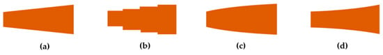
Figure 2. Schematic of the (a) linear; (b) multi-sectional; (c) parabolic; and (d) exponential Si inverse tapers (top view).
The multi-tip taper is widely applied to improve the modal overlap efficiency [45][46][47], and the schematic of a multi-tip taper is presented in Figure 3a. A superimposed mode can be formed at the taper facet of the single taper, which consists of multiple tips, and the modal field diameter (MFD) is thus increased to better match with the fiber mode regarding the aspect of modal size. The design parameters of a multi-tip taper include the number of tips, interval distance between adjacent tips, taper tip width, and taper length, which can be properly designed to achieve high modal overlap in different situations, and the shape of the multi-tip taper may resemble a fork or a comb. In the case of fiber-to-chip coupling, the edge coupler facet should be aligned with the fiber core accurately to ensure fine overlap; thus, coupling efficiency is highly sensitive to alignment condition. Since it is a set of multiple tips as a whole that interconnects with the fiber, the dependence on misalignment and fabrication deviation reduces, considering each single tip in a multi-tip taper coupler. A multi-tip taper with multiple tips can loosen the constraints of alignment and reach larger misalignment tolerance as well as fabrication deviation tolerance.
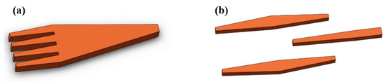
Figure 3. Schematic of Si photonic coupler based on (a) a multi-tip taper and (b) multiple tapers.
Inspired by the idea of the multi-tip taper, it is natural to propose another kind of edge coupler based on multiple tapers. The trident edge coupler with three separate tapers is the most common form among different types of edge couplers consisting of multiple tapers [48][49][50][51][52], and its structure is presented in Figure 3b. For trident edge couplers, light exiting from the fiber firstly enters the facet composed by two bilateral taper tips and is split into a superimposed mode due to the high refractive index contrast between Si and SiO2 when light continues to propagate along the edge coupler. A central Si taper appears and the mode exists in all the three tapers, and the proportion of mode confined by the central taper tends to increase as the width of the central taper becomes larger. Finally, when bilateral tapers end, the mode is totally converted into the central taper and then propagates into successive integrated circuits.
The concept of a subwavelength gratings structure (SWG) was proposed as an innovative concept in silicon photonic waveguide design more than one decade ago by researchers at the National Research Council of Canada [53] and has been widely adopted [54][55][56][57] due to its extraordinary characteristics in silicon photonic devices. The structure of a subwavelength grating is demonstrated in Figure 4a. As shown in Figure 4b, when the grating pitch is much larger than the wavelength, light is blocked by the Si blocks, and radiation happens at the facet, which prevents further light propagation along the grating. Only a certain component of light that satisfies the Bragg condition can go through the grating structure, which acts as a conventional diffraction grating. In circumstances where the wavelength and grating pitch are comparable in length, reflection occurs. As for gratings with small pitches under the subwavelength regime, light can directly propagate through the grating, as it behaves in a general continuous Si waveguide.
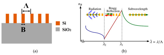
Figure 4. (a) Schematic of subwavelength gratings; (b) the relationship between effective index and wavelength-to-pitch ratio. Reproduced with permission from [58], Copyright John Wiley and Sons, 2014.
3.3. Structural Transformations of Edge Couplers in Vertical Direction
Typical silicon photonic integrated circuits are based on the SOI platform, which is composed of a thick silicon substrate, buried silicon dioxide for isolation, a photonic circuits layer, and top silica cladding for protection from bottom to top. It has the potential to make some changes in the vertical dimension within the buried silicon dioxide and the top cladding to improve the device performance. As for the vertical structural transformation of fiber-to-chip edge couplers, the main aim is to enlarge the effective modal area in the vertical direction to achieve a high modal match between the fiber core and the coupler facet. Figure 5shows an approach to obtain a large effective modal area where multiple waveguides are placed above the Si inverse taper [59][60]. Upper assisting waveguides are usually made of materials with a lower refractive index than silicon such as silicon nitride (SiN) and silicon oxynitride (SiON), which are also well compatible with the typical silicon photonic platform and CMOS fabrication process. Figure 5 demonstrates one type of pattern under which assisting multiple waveguides are introduced [61]. In principle, assisting waveguides should be placed above the appearance of an inverse taper so that the propagating mode distributed outside the narrow taper can be transmitted and confined upwards. Due to the existence of upper assisting waveguides with higher refractive indexes than the surrounding silicon dioxide cladding, light tends to be confined into the multiple assisting waveguides. Therefore, the lower Si inverse taper together with the upper assisting waveguides support a superimposed mode, and the modal area becomes enlarged and is comparable to that of the fiber core, which helps efficiently couple the light emitting from the fiber.
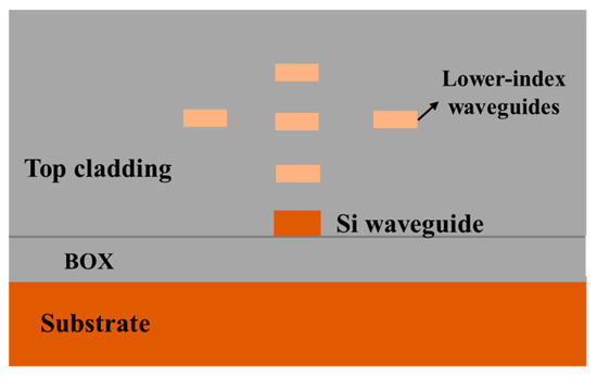
Figure 5. Silicon inverse taper assisted with multiple waveguides (cross-section view).
The last section shows the structural transformation of edge couplers in the vertical direction via assisting waveguides grown above the silicon inverse taper with an isolation layer of SiO2. Accordingly, it is also feasible to achieve a vertical transition of the propagating mode via cascaded tapers, as presented in Figure 6. An edge coupler based on multi-stage tapers consists of multiple unidirectional tapers in different layers with their wide end near the fiber and narrow end close to successive photonic waveguides. At the wide end where tapers in different layers merge, the edge coupler has a large cross-section area which is comparable with the fiber core, and light can couple into the coupler facet at a relatively low discrepancy. In the region of multi-stage tapers, the taper at the top layer has the shortest length, while the one at the bottom layer has the longest length. When light propagates in the cascaded multi-stage tapers and arrives at the first taper tip where the top-layer taper ends, light cannot be confined well in the top layer due to a too small cross-section area, and it inclines to transmit into the successive layer below, which has a higher refractive index than the surrounding SiO2 cladding. Likewise, light propagates in the second layer taper for a certain distance and then continues to transmit downwards when it propagates to the second taper tip until it reaches the bottom layer.
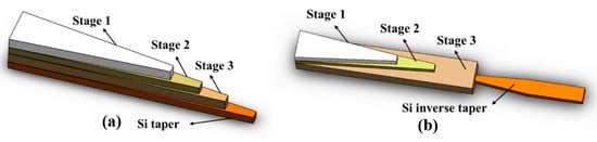
Figure 6. Two regimes of multi-stage tapers with (a) a forward taper and (b) an inverse taper.
Apart from edge couplers based on cascaded multi-stage tapers, there are also some research works about edge couplers with a Si inverse taper buried in index-matching claddings [62][63][64][65][66][67][68][69]. The typical structure of an edge coupler assisted with index-matching cladding is presented in Figure 7, and we can observe that unlike the Si layer underneath the SiO2 cladding, other kinds of materials including SiN, SiON, and polymers are utilized to engineer the refractive index between the value of the fiber core and silicon waveguides. In some cases, there may be an additional intermediate layer between the silicon waveguides and the top index-matching cladding.
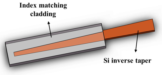
Figure 7. Sketch of silicon taper in index-matching cladding.
Typical tapers only have tapering profiles in the longitudinal and lateral dimension, while the thickness of the taper stays constant. However, it is possible to transmit light from the fiber through a three-dimensional taper (3D taper) that can gradually converge. As shown in Figure 8a, a 3D taper is aligned to fiber with its wide end, which is comparable with the fiber core in the aspect of structure size. Then, it begins to taper in both the vertical and horizontal dimensions to connect with the silicon waveguide. Generally, three-dimensional tapers can be divided into two main types: one is purely silicon-based 3D tapers, and the other is 3D tapers assisted with other kinds of intermedium materials. As for the purely silicon-based 3D tapers [70][71][72][73], there are also two different approaches to adjust the three-dimensional profile. In some previous works [70][73], the wide end of the taper becomes narrower in both the vertical and lateral directions until it forms a narrow end with the same thickness and width as the silicon waveguide as presented in Figure 8b. In some other works [71][72], the 3D taper firstly begins to reduce in thickness while the width remains unchanged. Then, the 3D taper transits into a thin silicon slab with the same thickness as the silicon waveguide, and then the lateral slab gradually tapers similar to a traditional two-dimensional taper, which connects with the silicon waveguide afterwards, as shown in Figure 8c.
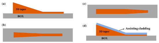
Figure 8. (a) Diagram of a Si 3D taper (side view); (b) and (c) two types of 3D taper profile (top view); (d) a 3D taper assisted with other material.
Several forms of vertical transformation of edge couplers have been depicted in previous sections including couplers assisted with multiple waveguides, couplers based on cascaded multi-stage tapers, couplers with index-matching cladding, and couplers based on three-dimensional tapers. Basically, these edge couplers have additionally designed structures upon the Si inverse taper. Typical SOI wafers use thick silicon as the substrate and grow a layer of silicon dioxide with a thickness of several microns as the buried oxide layer to isolate the device layer with the substrate. Intuitively, it is also applicable to design specific structures below the Si inverse taper. Cantilevers structures are commonly used in micro-electro-mechanical systems (MEMS), and they also play important roles in edge coupler design [74][75][76][77][78]. The schematic of such a structure is demonstrated in Figure 9. Based on initial single Si inverse taper, the BOX layer and the substrate underneath the BOX layer are partly undercut to a certain thickness, and a suspended beam of Si taper cladded with SiO2 is exposed. Several supporting beams are set to sustain the suspended arm to enable structure stability. A fiber is placed in the etched slot and aligned with the cleaved facet of the cantilever arm.
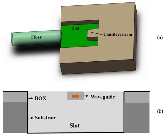
Figure 9. (a) Typical structure of edge couplers with cantilever; (b) cross-section of the cantilever.
4. Conclusion
Research works in recent years have witnessed the significance and practicality of silicon photonics in the field of photonic integrated chips. Optical interconnects in silicon photonic integrated circuits is a critical issue to focus on to achieve efficient data transmission. The two mainstream paradigms of fiber-to-chip optical interconnects, namely vertical coupling and edge coupling, have different characteristics, while edge coupling is superior in the aspects of higher coupling efficiency, broader operation bandwidth, and lower dependence on polarization status.
This entry is adapted from the peer-reviewed paper 10.3390/app10041538
References
- Jalali, B.; Fathpour, S. Silicon photonics. J. Lightwave Technol. 2006, 24, 4600–4615.
- Soref, R. The past, present, and future of silicon photonics. IEEE J. Sel. Top. Quant. 2006, 12, 1678–1687.
- Xu, D.X.; Schimid, J.H.; Reed, G.T.; Mashanovich, G.Z.; Thomson, D.J.; Nedeljkovic, M.; Chen, X.; Thourhout, D.V.; Keyvaninia, S.; Selvaraja. S.K. Silicon photonic integration platform—have we found the sweet spot? IEEE J. Sel. Top. Quant. 2014, 20, 189–205.
- Thomson, D.; Zilkie, A.; Bowers, J.E.; Komljenovic, T.; Reed, G.T.; Vivien, L.; Marris-Morini, D.; Cassan, E.; Virot, L.; Fédéli, J.-M.; et al. Roadmap on silicon photonics. J. Optics 2016, 18, 073003.
- Chen, X.; Milosevic, M.M.; Stankovic, S.; Reynolds, S.; Bucio, T.D.; Li, K.; Thomson, D.J.; Gardes, F.; Reed, G.T. The emergence of silicon photonics as a flexible technology platform. P. IEEE 2018, 106, 2101–2116.
- Xiao, X.; Li, Z.; Chu, T.; Xu, H.; Li, X.; Nemkova, A.; Kang, X.; Yu, Y.; Yu, J. Development of silicon photonic devices for optical interconnects. Sci. China Technol. Sci. 2013, 56, 586–593.
- Chen, X.; Li, C.; Tsang, H.K. Device engineering for silicon photonics. NPG Asia Mater. 2011, 3, 34–40.
- Subbaraman, H.; Xu, X.; Hosseini, A.; Zhang, X.; Zhang, Y.; Kwong, D.; Chen, R.T. Recent advances in silicon-based passive and active optical interconnects. Opt. Express 2015, 23, 2487–2510.
- Son, G.; Han, S.; Park, J.; Kwon, K.; Yu, K. High-efficiency broadband light coupling between optical fibers and photonic integrated circuits. Nanophotonics 2018, 7, 1845–1864.
- Vermeulen, D.; Poulton, C.V. Optical interfaces for silicon photonic circuits. P. IEEE 2018, 106, 2270–2280.
- Sunak, H.R.D. Single-mode fiber measurements. IEEE Insrtu. Meas. 1988, 37, 557–560.
- Dutta, H.S.; Goyal, A.K.; Srivastava, V.; Pal, S. Coupling light in photonic crystal waveguides: A review. Photonic. Nanostruct. 2016, 20, 41–58.
- Marchetti, R.; Lacava, C.; Carroll, L.; Gradkowski, K.; Minzioni, P. Coupling strategies for silicon photonics integrated chips. Photonics Res. 2019, 7, 201–239.
- Feng, J.; Zhou, Z. Polarization beam splitter using a binary blazed grating coupler. Opt. Lett. 2017, 32, 1662–1664.
- Xiao, Z.; Luan, F.; Liow, T.Y.; Zhang, J.; Shum, P. Design for broadband high-efficiency grating couplers. Opt. Lett. 2012, 37, 530–532.
- Qin, K.; Gao, D.; Bao, C.; Zhao, Z.; Zhou, X.; Lu, T.; Chen, L. High efficiency and broadband two-dimensional blazed grating coupler with fully etched triangular holes. J. Lightwave Technol. 2012, 30, 2363–2366.
- Xu, D.X.; Cheben, P.; Dalacu, D.; Delâge, A.; Janz, S.; Lamontagne, B.; Picard, M.J.; Ye, W.N. Eliminating the birefringence in silicon-on-insulator ridge waveguides by use of cladding stress. Opt. Lett. 2004, 29, 2384–2386.
- Bozzola, A.; Carroll, L.; Gerace, D.; Cristiani, I.; Andreani, L.C. Optimising apodized grating couplers in a pure SOI platform to -0.5 dB coupling efficiency. Opt. Express 2015, 23, 16289–16304.
- Zhang, J.; Yang, J.; Lu, H.; Wu, W.; Huang, J.; Chang, S. Polarization-independent grating coupler based on silicon-on-insulator. Chin. Opt. Lett. 2015, 13, 091301–091305.
- Wang, Y.; Shi, W.; Wang, X.; Lu, Z.; Caverley, M.; Bojko, R.; Chrostowski, L.; Jaeger, N.A. Design of broadband subwavelength grating couplers with low back reflection. Opt. Lett. 2015, 40, 4647–4650.
- Watanabe, T.; Ayata, M.; Koch, U.; Fedoryshyn, Y.; Leuthold, J. Perpendicular grating coupler based on a blazed antiback-reflection structure. J. Lightwave Technol. 2017, 35, 4663–4669.
- Wang, Y.; Yun, H.; Lu, Z.; Bojko, R.; Shi, W.; Wang, X.; Flueckiger, J.; Zhang, F.; Caverley, M.; Jaeger, N.A.F.; et al. Apodized focusing fully etched subwavelength grating couplers. IEEE Photonics J. 2015, 7, 1–10.
- Ho, C.P.; Zhao, Z.; Li, Q.; Takagi, S.; Takenaka, M. Tunable grating coupler by thermal actuation and thermo-optic effect. IEEE Photonic. Tech. L. 2018, 30, 1503–1506.
- Papes, M.; Cheben, P.; Benedikovic, D.; Schmid, J.H.; Pond, J.; Halir, R.; Ortega-Monux, A.; Wanguemert-Perez, G.; Ye, W.N.; Xu, D.X.; et al. Fiber-chip edge coupler with large mode size for silicon photonic wire waveguides. Opt. Express 2016, 24, 5026–5038.
- Romero-Garcia, S.; Marzban, B.; Merget, F.; Shen, B.; Witzens, J. Edge couplers with relaxed alignment tolerance for pick-and-place hybrid integration of III–V lasers with SOI waveguides. IEEE J. Sel. Top. Quant. 2014, 20, 369–379.
- Tao, S.H.; Song, J.; Fang, Q.; Yu, M.B.; Lo, G.Q.; Kwong, D.L. Improving coupling efficiency of fiber-waveguide coupling with a double-tip coupler. Opt. Express 2008, 16, 20803–20808.
- Hatori, N.; Shimizu, T.; Okano, M.; Ishizaka, M.; Yamamoto, T.; Urino, Y.; Mori, M.; Nakamura, T.; Arakawa, Y. A hybrid integrated light source on a silicon platform using a trident spot-size converter. J. Lightwave Technol. 2014, 32, 1329–1336.
- Lai, Y.; Yu, Y.; Fu, S.; Xu, J.; Shum, P.P.; Zhang, X. Efficient spot size converter for higher-order mode fiber-chip coupling. Opt. Lett. 2017, 42, 3702–3705.
- Yasuhara, K.; Yu, F.; Tshigure, T. Polymer waveguide based spot-size converter for low-loss coupling between Si photonics chips and single-mode fibers. In Proceedings of the 2017 Optical Fiber Communications Conference and Exhibition (OFC), Los Angeles, CA, USA, 19 March 2017.
- Snyder, B.; Lepage, G.; Balakrishnan, S.; Verheyen, P.; Pantouvaki, M.; Absil, P.; Campenhout, J.V. Broadband, polarization-insensitive lensed edge couplers for silicon photonics. In Proceedings of the 2018 IEEE 68th Electronic Components and Technology Conference (ECTC), San Diego, CA, USA, 29 May 2018.
- Jia, L.; Li, C.; Liow, T.-Y.; Lo, G.-Q. Efficient suspended coupler with loss less than −1.4 dB between Si-photonic waveguide and cleaved single mode fiber. J. Lightwave Technol. 2018, 36, 239–244.
- Larrea, R.; Gutierrez, A.M.; Griol, A.; Brimont, A.; Sanchis, P. Fiber-to-chip spot-size converter for coupling to silicon waveguides in the O-band. IEEE Photonic. Tech. L. 2019, 31, 31–34.
- Cardenas, J.; Luke, K.; Luo, L.W.; Poitras, C.B.; Morton, P.A.; Lipson, M. High coupling efficiency etched facet tapers in silicon. In Proceedings of 2012 Conference on Lasers and Electro-Optics, San Jose, CA, USA, 06 May 2012.
- Chuang, S. Physics of Photonic Devices, 2nd ed.; John Wiley & Sons, Inc.: Hoboken, NJ, USA, 2009; pp. 273–279.
- Chrostowski, L.; Hochberg, M. Silicon Photonics Design: From Devices to Systems, 1st ed.; Cambridge University Press: Cambridge, UK, 2015; pp. 10–14.
- Dong, P.; Preble, S.F.; Robinson, J.T.; Manipatruni, S.; Lipson, M. Inducing photonic transitions between discrete modes in a silicon optical microcavity. Phys. Rev. Lett. 2008, 100, 033904.
- Stern, B.; Zhu, X.; Chen, C.P.; Tzhuang, L.D.; Cardenas, J.; Bergman, K.; Lipsonm, M. On-chip mode-division multiplexing switch. Optica 2015, 2, 530–535.
- He, Y.; Zhang, Y.; Zhu, Q.; An, S.; Cao, R.; Guo, X.; Qiu, C.; Su, Y. Silicon High-Order Mode (De)Multiplexer on Single Polarization. J. Lightwave Technol. 2018, 36, 5746–5753.
- Kopp, C.; Bernabé, S.; Bakir, B.B.; Fedeli, J.M.; Orobtchouk, R.; Schrank, F.; Porte, H.; Zimmermann, L. Silicon photonic circuits: On-CMOS integration, fiber optical coupling, and packaging. IEEE J. Sel. Top. Quant. 2011, 17, 498–509.
- Fu, Y.; Ye, T.; Tang, W.; Chu, T. Efficient adiabatic silicon-on-insulator waveguide taper. Photonics Res. 2014, 2, 41–44.
- Suchoski, P.; Ramaswamy, R. Design of single-mode step-tapered waveguide sections. IEEE J. Sel. Top. Quant. 1987, 23, 205–211.
- Wang, J.; Qi, M.; Xuan, Y.; Huang, H.; Li, Y.; Li, M.; Chen, X.; Jia, Q.; Sheng, Z.; Wu, A.; et al. Proposal for fabrication-tolerant SOI polarization splitter-rotator based on cascaded MMI couplers and an assisted bi-level taper. Opt. Express 2014, 22, 27869–27879.
- Hettrick, S.J.; Wang, J.; Li, C.; Wilkinson, J.S.; Shepherd, D.P. An experimental comparison of linear and parabolic tapered waveguide lasers and a demonstration of broad-stripe diode pumping. J. Lightwave Technol. 2004, 22, 845–849.
- Ren, G.; Chen, S.; Cheng, Y.; Zhai, Y. Study on inverse taper based mode transformer for low loss coupling between silicon wire waveguide and lensed fiber. Opt. Commun. 2011, 284, 4782–4788.
- Liu, Y.; Yu, J. Low-loss coupler between fiber and waveguide based on silicon-on-insulator slot waveguides. Appl. Opt. 2007, 46, 7858–7861.
- Tu, X.; Fu, H.; Geng, D. Y-branch edge coupler between cleaved single mode fiber and nano-scale waveguide on silicon-on-insulator platform. In Proceedings of the 2014 Asia Communications and Photonics Conference, Shanghai, China, 11 November 2014.
- Mu, X.; Wu, S.; Cheng, L.; Tu, X.; Fu, H. High-performance silicon nitride fork-shape edge coupler. In Proceedings of the 2019 Frontiers in Optics; Washington, DC, USA, 15 September 2019.
- Hatori, N.; Urino, Y.; Shimizu, T.; Okano, M.; Yamamoto, T.; Mori, M.; Nakamura, T.; Arakawa, Y. Quantum dot laser for a light source of an athermal silicon optical interposer. Photonics 2015, 2, 355–364.
- Itoh, K.; Kuno, Y.; Hayashi, Y.; Suzuki, J.; Hojo, N.; Amemiya, T.; Nishiyama, N.; Arai, S. Crystalline/amorphous Si integrated optical couplers for 2D/3D interconnection. IEEE J. Sel. Top. Quant. 2016, 22, 255–263.
- Hatori, N.; Shimizu, T.; Okano, M.; Ishizaka, M.; Yamamoto, T.; Urino, Y.; Mori, M.; Nakamura, T.; Arakawa, Y. A novel spot size convertor for hybrid integrated light sources on photonics-electronics convergence system. In Proceedings of the 2012 IEEE 9th International Conference on Group IV Photonics (GFP), San Diego, CA, USA, 29 August 2012.
- Tu, X.; Dumain, P.; Li, M.; Goodwill, D.; Fu, H.; Geng, D.; Bernier, E. Low polarization-dependent-loss silicon photonic trident edge coupler fabricated by 248 nm optical lithography. In Proceedings of the 2015 Asia Communications and Photonics Conference, Hongkong, Hongkong, 19 November 2015.
- Mu, X.; Wu, S.; Cheng, L.; Tu, X.; Fu, H.Y. A compact adiabatic silicon photonic edge coupler based on silicon nitride/silicon trident structure. In Proceedings of the 2019 18th International Conference on Optical Communications and Networks (ICOCN), Huangshan, China, 5 August 2019.
- Cheben, P.; Xu, D.X.; Janz, S.; Densmore, A. Subwavelength waveguide grating for mode conversion and light coupling in integrated optics. Opt. Express 2006, 14, 4695–4702.
- Cheben, P.; Bock, P.J.; Schimid, J.H.; Lapointe, J.; Janz, S.; Xu, D.X.; Densmore, A.; Delâge, A.; Lamontagne, B.; Hall, T.J. Refractive index engineering with subwavelength gratings for efficient microphotonic couplers and planar waveguide multiplexers. Opt. Lett. 2010, 35, 2526–2528.
- Bock, P.J.; Cheben, P.; Schmid, J.H.; Lapointe, J.; Delâge, A.; Janz, S.; Aers, G.C.; Xu, D.X.; Densmore, A.; Hall, T.J. Subwavelength grating periodic structures in silicon-on-insulator: A new type of microphotonic waveguide. Opt. Express 2010, 18, 20251–20262.
- Donzella, V.; Sherwali, A.; Flueckiger, J.; Talebi Fard, S.; Grist, S.M.; Chrostowski, L. Sub-wavelength grating components for integrated optics applications on SOI chips. Opt. Express 2014, 22, 21037–21050.
- Cheben, P.; Schmid, J.H.; Wang, S.; Xu, D.X.; Vachon, M.; Janz, S.; Lapointe, J.; Painchaud, Y.; Picard, M.J. Broadband polarization independent nanophotonic coupler for silicon waveguides with ultra-high efficiency. Opt. Express 2015, 23, 22553–22563.
- Halir, R.; Bock, P.J.; Cheben, P.; Ortega-Moñux, A.; Alonso-Ramos, C.; Schmid, J.H.; Lapointe, J.; Xu, D.-X.; Wangüemert-Pérez, J.G.; Molina-Fernández, Í.; et al. Waveguide sub-wavelength structures: A review of principles and applications. Laser Photonics Rev. 2015, 9, 25–49.
- Picard, M.J.; Latrasse, C.; Larouche, C.; Painchaud, Y.; Poulin, M.; Pelletier, F.; Guy, M. CMOS-compatible spot-size converter for optical fiber to sub-um silicon waveguide coupling with low-loss low-wavelength dependence and high tolerance to misalignment. In Proceedings of the SPIE OPTO, San Francisco, CA, USA, 14 March 2016.
- Sisto, M.M.; Fisette, B.; Paultre, J.E.; Paquet, A.; Desroches, Y. Novel spot size converter for coupling standard single mode fibers to SOI waveguides. In Proceedings of the SPIE OPTO, San Francisco, CA, USA, 14 March 2016.
- Voigt, K.; Brulis, V.; Petermann, K.; Zimmermann, L. Study of backend waveguide arrays for adiabatic coupling to Si waveguides. In Proceedings of the 2017 IEEE 14th International Conference on Group IV Photonics (GFP), Berlin, Germany, 23 August 2017.
- Lee, J.-M.; Kim, D.-J.; Ahn, H.; Park, S.-H.; Kim, G. Temperature dependence of silicon nanophotonic ring resonator with a polymeric overlayer. J. Lightwave Technol. 2007, 25, 2236–2243.
- Pu, M.; Liu, L.; Ou, H.; Yvind, K.; Hvam, J.M. Ultra-low-loss inverted taper coupler for silicon-on-insulator ridge waveguide. Opt. Commun. 2010, 283, 3678–3682.
- Ben Bakir, B.; de Gyves, A.V.; Orobtchouk, R.; Lyan, P.; Porzier, C.; Roman, A.; Fedeli, J.M. Low-loss (<1 dB) and polarization-insensitive edge fiber couplers fabricated on 200-mm silicon-on-insulator wafers. IEEE Photonic. Tech. L. 2010, 22, 739–741.
- Raghunathan, V.; Yagüe, J.L.; Xu, J.; Michel, J.; Gleason, K.K.; Kimerling, L.C. Co-polymer clad design for high performance athermal photonic circuits. Opt. Express 2012, 20, 20808–20813.
- Ku, K.-N.; Lee, M.-C.M. Wide-band optical mode converters for coupling between fibers and silicon photonic wires with large misalignment tolerance. J. Lightwave Technol. 2013, 31, 1616–1620.
- Jia, L.; Song, J.; Liow, T.Y.; Luo, X.; Tu, X.; Fang, Q.; Koh, S.C.; Yu, M.; Lo, G. Mode size converter between high-index-contrast waveguide and cleaved single mode fiber using SiON as intermediate material. Opt. Express 2014, 22, 23652–23660.
- Takei, R.; Maegami, Y.; Omoda, E.; Sakakibara, Y.; Mori, M.; Kamei, T. Low-loss and low wavelength-dependence vertical interlayer transition for 3D silicon photonics. Opt. Express 2015, 23, 18602–18610.
- Maegami, Y.; Takei, R.; Omoda, E.; Amano, T.; Okano, M.; Mori, M.; Kamei, T.; Sakakibara, Y. Spot-size converter with a SiO2 spacer layer between tapered Si and SiON waveguides for fiber-to-chip coupling. Opt. Express 2015, 23, 21287–21295.
- Fritze, M.; Knecht, J.; Bozler, C.; Keast, C.; Fijol, J.; Jacobson, S.; Keating, P.; LeBlanc, J.; Fike, E.; Kessler, B.; et al. Fabrication of three-dimensional mode converters for silicon-based integrated optics. J. Vac. Sci. Technol. B 2003, 21, 2897–2902.
- Holly, R.; Hingerl, K.; Merz, R.; Hudek, P. Fabrication of silicon 3D taper structures for optical fibre to chip interface. Microelectron. Eng. 2007, 84, 1248–1251.
- Shiraishi, K.; Yoda, H.; Ohshima, A.; Ikedo, H.; Tsai, C.S. A silicon-based spot-size converter between single-mode fibers and Si-wire waveguides using cascaded tapers. Appl. Phys. Lett. 2007, 91, 141120.
- Takei, R.; Suzuki, M.; Omoda, E.; Manako, S.; Kamei, T.; Mori, M.; Sakakibara, Y. Silicon knife-edge taper waveguide for ultralow-loss spot-size converter fabricated by photolithography. Appl. Phys. Lett. 2013, 102, 101108.
- Fang, Q.; Liow, T.S.; Song, J.; Tan, C.; Yu, M.; Lo, G.; Kwong, D.L. Suspended optical fiber-to-waveguide mode size converter for Silicon photonics. Opt. Express 2010, 18, 7763–7769.
- Chen, L.; Doerr, C.R.; Chen, Y.-K.; Liow, T.-Y. Low-loss and broadband cantilever couplers between standard cleaved fibers and high-index-contrast Si3N4 or Si Waveguides. IEEE Photonic. Tech. L. 2010, 22, 1744–1746.
- Fang, Q.; Song, J.; Luo, X.; Yu, M.; Lo, G.; Liu, Y. Mode-size converter with high coupling efficiency and broad bandwidth. Opt. Express 2011, 19, 21588–21594.
- Wood, M.; Sun, P.; Reano, R.M. Compact cantilever couplers for low-loss fiber coupling to silicon photonic integrated circuits. Opt. Express 2012, 20, 164–172.
- Jia, L.; Song, J.; Liow, T.S.; Luo, X.; Tu, X.; Fang, Q.; Koh, S.C.; Yu, M.; Lo, G. Low loss/large tolerance mode converter between SiN waveguide and cleaved single mode fiber. In Proceedings of the 2014 Optical Fiber Communications Conference and Exhibition (OFC), San Francisco, CA, USA, 9 March 2014.