Silicon photonics has drawn increasing attention since recent decades and is promising to act as a key technology for future daily applications due to its various merits including ultra-low cost, high integration density owing to the high refractive index of silicon and compatibility with current semiconductor fabrication process. Optical interconnects is an important issue in silicon photonic integrated circuits to transmit light and fiber-to-chip optical interconnects is vital in application scenarios like data centers and optical transmission systems. There are mainly two categories of fiber-to-chip optical coupling, that is off-plane coupling and in-plane coupling. Grating couplers work under the former category while edge couplers function as in-plane coupling. In this paper, we mainly focus on edge couplers in silicon photonic integrated circuits. We deliver an introduction to the research background, operation mechanism and design principles of silicon photonic edge couplers. The state-of-the-art of edge couplers is reviewed according to different configurations as to the device structure, identifying the performance, fabrication feasibility and applications. In addition, a brief comparison between edge couplers and grating couplers is conducted. Packaging issue is also discussed and several prospective techniques for further improvements of edge couplers are proposed.
- silicon photonics
- optical interconnects
- fiber-to-chip coupling
- edge couplers
- inverse taper
1. Definition
Silicon photonics has drawn increasing attention in the past few decades and is a promising key technology for future daily applications due to its various merits including ultra-low cost, high integration density owing to the high refractive index of silicon, and compatibility with current semiconductor fabrication process. Optical interconnects is an important issue in silicon photonic integrated circuits for transmitting light, and fiber-to-chip optical interconnects is vital in application scenarios such as data centers and optical transmission systems. There are mainly two categories of fiber-to-chip optical coupling: off-plane coupling and in-plane coupling. Grating couplers work under the former category, while edge couplers function as in-plane coupling.
2. Introduction
As the size of electronic integrated circuits scales down to the physical limit and the demand for high data rates rises tremendously, photonic integrated circuits (PIC) has gradually taken the stage due to its inherent high speed and low power consumption. Silicon has the potential to construct compact devices benefiting from its high refractive index, and silicon-based devices are well compatible with current mature and standardized complementary metal oxide semiconductor (CMOS) platform. Thus, silicon is a promising material for novel PIC, and silicon photonics has been a hot research topic in recent years [1,2,3,4,5]. In cases of complex optical transmission systems, optical interconnects between fiber and the photonic integrated circuits happen frequently in the whole system [6], so efficient fiber-to-chip coupling is an important factor to pay attention to for system performance [7,8,9,10]. To date, the feature size of silicon waveguide can be as tiny as tens of nanometers while the typical diameter of a single mode fiber (SMF) is around 125 μm with a core diameter near 10 μm [11]. Figure 1 shows the huge size mismatch between a fiber core and the Si waveguide, which causes considerable optical transmission loss when light emitting from the fiber core enters the Si waveguide directly. Fiber-to-chip couplers are a type of key photonic component to deal with this issue in optical interconnects.
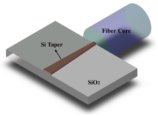
Figure 1. Schematic of optical interconnects between fiber and photonic chip.
3. Data, Model, Applications and Influences
3.1. Operation Mechanism and Design Principles of Edge Couplers
Fiber-to-chip edge couplers have been widely investigated by researchers for decades, and the inverse taper structure plays an indispensable role in edge coupling [33]. Corresponding to the direction of light propagation, inverse taper refers to a tapering waveguide with a gradual increase in width along the mode propagation direction, which means the narrow end of the taper is close to fiber, while the wide end is connected with photonic waveguides. Modal distribution is determined by both the mode order and the waveguide structure. For a specific mode, only waveguides with a certain cross-section area can support the entire mode [34]. The fundamental transverse electric (TE) mode is mostly applied in optical communication applications to transmit information, and most of the researches on silicon photonic edge couplers studied the transverse electric mode. The most commonly used size of silicon photonic waveguide that can support the fundamental TE mode propagation at negligible loss is about 200 nanometers high and about 500 nanometers wide [35]. A waveguide with a too small cross-section area cannot support an entire fundamental mode, and thus the mode will partially distribute in the outer region of the waveguide. In contrast, a waveguide with a too large cross-section area will easily excite undesirable higher-order modes [36,37,38]. The taper is just appropriate for mode conversion, since a gradually varying cross-section area supports mode transformation and mode size variation. On this basis, the narrow end of the inverse taper has a smaller cross-section area than the expected modal size, so it is unable to confine the incident mode completely, and a considerable percentage of the electromagnetic field distributes surrounding the taper tip. As the taper width becomes larger, it can support the entire mode and confine the electromagnetic field inside the taper integrally. Overall, an edge coupler based on an inverse taper whose narrow tip is aligned to the fiber core can convert a large mode incident from the optical fiber to the compressed guided mode in photonic waveguides.
When evaluating the performance of an edge coupler, there are some general metric parameters including coupling efficiency (or coupling loss), device footprint, operating bandwidth, fabrication deviation tolerance, and misalignment tolerance [39]. Coupling efficiency is the most critical and fundamental parameter for an edge coupler, indicating the ratio of output power over the input power after light transmission and mode conversion inside the edge coupler. To achieve a high coupling efficiency is the main goal in designing optical couplers. The device footprint is another important parameter to define the advantage of an edge coupler considering the integration density, fabrication feasibility, and packing difficulty. Photonic devices with a compact size are desired for improving the integration density and reducing the cost. Since edge couplers generally consist of tapers that are longitudinal shaped, the main idea of achieving a compact edge coupler is to decrease the device length. When it comes to wavelength characteristics, an edge coupler has the inherent advantage of broad operating bandwidth, since it works based on the propagation property of light rather than the diffraction effect of light in grating couplers. The broad operating bandwidth implies that the edge coupler can work efficiently and stably in a wide wavelength range, insensitive to wavelength fluctuation. In addition, due to the structural symmetry and simplicity, edge couplers based on a single taper are easy and straightforward to fabricate and have good fabrication deviation tolerance and misalignment tolerance.
3.2. Structural Transformations of Edge Couplers in Horizontal Direction
An edge coupler based on one standard single inverse taper is the most basic and straightforward formation for all various types of edge couplers. When the thickness of the Si waveguide is constant while the width decreases gradually toward the fiber, the Si strip waveguide becomes a taper. Light cannot be confined properly within the narrow taper end. Thus, the mode is distributed in a larger area around the taper, which contributes to an enlarged modal size. As light emitting from the fiber is coupled into the Si taper and continues to travel along the widening taper, the mode tends to be better confined by the larger cross-section and can propagate with ultra-low loss into successive devices. As presented in Figure 2a, the linear profile is the most common form considering the contour of the inverse taper, but it may be not the most appropriate form to achieve the best performance. The main advantage of a linear-taper coupler is its simple structure and ease of fabrication, while this structural simplicity also leads to an extremely large size and limited coupling efficiency, especially for optical coupling to fibers with a large spot size. Research studies on different profiles of tapers have been conducted to realize better performance compared with linear-shape tapers in the aspects of smaller footprint, lower propagation loss, and broader bandwidth. Common transformations of linear tapers include multi-sectional tapers [49,51,52], parabolic tapers or quadratic tapers [53], and exponential tapers [54], as shown in Figure 2b–d separately. The mode propagation loss is dependent on multiple factors including taper length, taper tip width, and the slope of the contour profile.

Figure 2. Schematic of the (a) linear; (b) multi-sectional; (c) parabolic; and (d) exponential Si inverse tapers (top view).

3.3. Structural Transformations of Edge Couplers in Vertical Direction
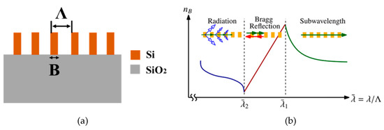
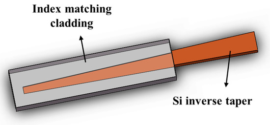
Typical silicon photonic integrated circuits are based on the SOI platform, which is composed of a thick silicon substrate, buried silicon dioxide for isolation, a photonic circuits layer, and top silica cladding for protection from bottom to top. It has the potential to make some changes in the vertical dimension within the buried silicon dioxide and the top cladding to improve the device performance. As for the vertical structural transformation of fiber-to-chip edge couplers, the main aim is to enlarge the effective modal area in the vertical direction to achieve a high modal match between the fiber core and the coupler facet. Figure 5shows an approach to obtain a large effective modal area where multiple waveguides are placed above the Si inverse taper [74,75]. Upper assisting waveguides are usually made of materials with a lower refractive index than silicon such as silicon nitride (SiN) and silicon oxynitride (SiON), which are also well compatible with the typical silicon photonic platform and CMOS fabrication process. Figure 5 demonstrates one type of pattern under which assisting multiple waveguides are introduced [76]. In principle, assisting waveguides should be placed above the appearance of an inverse taper so that the propagating mode distributed outside the narrow taper can be transmitted and confined upwards. Due to the existence of upper assisting waveguides with higher refractive indexes than the surrounding silicon dioxide cladding, light tends to be confined into the multiple assisting waveguides. Therefore, the lower Si inverse taper together with the upper assisting waveguides support a superimposed mode, and the modal area becomes enlarged and is comparable to that of the fiber core, which helps efficiently couple the light emitting from the fiber.
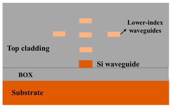
Figure 5. Silicon inverse taper assisted with multiple waveguides (cross-section view).


4. Conclusion
Research works in recent years have witnessed the significance and practicality of silicon photonics in the field of photonic integrated chips. Optical interconnects in silicon photonic integrated circuits is a critical issue to focus on to achieve efficient data transmission. The two mainstream paradigms of fiber-to-chip optical interconnects, namely vertical coupling and edge coupling, have different characteristics, while edge coupling is superior in the aspects of higher coupling efficiency, broader operation bandwidth, and lower dependence on polarization status.
This entry is adapted from the peer-reviewed paper 10.3390/app10041538
