Printed electronics are manufactured in a process of registering thin functional material (ink) layer combinations on a low-cost substrate that may be recycled and/or naturally degraded in nature. Correspondingly, the manufacturing process is composed of three complementary stages: material selection, printing and post-printing. The materials for the printed electronics are principally inks of conducting, semiconducting or dielectric characteristics and substrates, which are derived from synthetic or natural polymers. The inks are transferred with a master through direct contact to the substrate in case of contact printing, while they are deposited onto the substrate typically through nozzles in case of non-contact printing. Posterior to the printing process, it is often necessary to conduct sintering/curing in order to reach the desired functional ink and substrate characteristics. The inks, substrate and the printing technology along with the post printing requirements must be carefully evaluated for quality, repeatability and life-time aspects of the yield.
- printed electronics
- industrial automation
- information and communication technologies (ICT)
- monitoring and sensing technologies
1. Introduction
Printed electronics has a great potential to offer biodegradable and recyclable solutions, which is a way forward to minimize the electronic waste (e-waste) caused by the ever-increasing number of disposable electronic devices [1][2]. As the demand toward adding intelligence to the objects from our daily life has recently increased, the environmental impact of electronics manufacturing has reached to a significant level. Additive Manufacturing (AM) of these devices, e.g., by conventional and the state-of-the-art printing methods, relieves this impact by decreasing used (and wasted) materials and by allowing manufacturing to be completed without the need for etching and masking [3]. AM not only improves the resource efficiency but also reduces the fabrication costs since these manufacturing processes remain the same for both design prototyping and their mass production [4]. In addition, the recent advances also prove that AM methods can be used in hybrid printed electronic circuit fabrication, for which the conventional surface-mount technology (SMT) components are adhesively bonded to the printed substrates [5][6]. The full potential of using AM for electronic component manufacturing will be reached by replacing all SMT components with their printed counterparts as the assembly process may be completely eliminated [7][8][9]. Therefore, in the future, the electronic components and devices used in the fields of communication, energy and biomedicine can be viably and sustainably manufactured using various printing technologies [10].
Printed electronics are manufactured in a process of registering thin functional material (ink) layer combinations on a low-cost substrate that may be recycled and/or naturally degraded in nature. Correspondingly, the manufacturing process is composed of three complementary stages: material selection, printing and post-printing, as depicted in Figure 1. The materials for the printed electronics are principally inks of conducting, semiconducting or dielectric characteristics and substrates, which are derived from synthetic or natural polymers. The inks are transferred with a master through direct contact to the substrate in case of contact printing, while they are deposited onto the substrate typically through nozzles in case of non-contact printing. Posterior to the printing process, it is often necessary to conduct sintering/curing in order to reach the desired functional ink and substrate characteristics. The inks, substrate and the printing technology along with the post printing requirements must be carefully evaluated for quality, repeatability and life-time aspects of the yield.
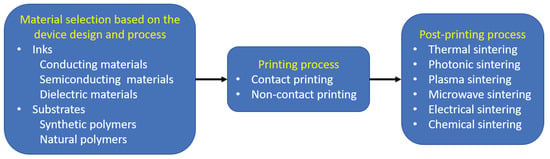
Figure 1. Complementary steps for electronics printing.
Although the requirements for the mass production of printed electronics with the desired specifications are challenging, the current state-of-the-art for the materials, fabrication processes and inspection technologies demonstrate an increasing trend in both repeatability and functional performance [11]. Undoubtedly, continuous growth of biodegradable and recyclable material portfolios for conductive, semiconductor and dielectric inks, and synthetic and natural polymeric substrates are fostered by the printing and post-treatment technologies, and optical inspection systems [12][13]. As a result, printing methods have gained a ground for large area fabrication of flexible electronics including radio frequency identification (RFID) devices; photovoltaic cells; organic light-emitting diodes (OLEDs); thin film transistors (TFTs); diodes; displays; batteries; and sensors measuring temperature, humidity and pH levels [14][15][16][17]. These developments demonstrate that reliable and repeatable solutions for the mass production of printed electronics with well-defined manufacturing standards will be available in very near future. In this study, we present the printing principles and approaches by surveying the recent investigations in the manufacturing and material technologies, applications and environmental impacts
2. Printing Technologies
Printing technologies, as a part of the additive manufacturing umbrella, have been extending electronics designers toolbox with access to various materials and ability to apply unorthodox structures in their designs. While printing of all the components is the ultimate aim of the electronics printing, most of the research activities are related to design and manufacturing of individual electronic components. Especially, their low manufacturing cost, large-area processability and lower carbon footprints compared with their conventional counterparts has attracted significant interest from the scientific and industrial communities. The printed electronic devices also provide favorable physical characteristics, e.g., low weight, stretching, resistance to folding or bending, which can not be realized with the conventional electronics [18][19].
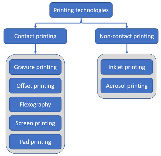
The technologies used for printing electronic components are well-known in the graphic arts. Some examples are gravure printing, flexography, offset printing, screen printing and inkjet printing as depicted in Figure 2. These technologies are often grouped into contact printing processes, which use printing master [20], contactless (non impact) printing processes that do not need a master [21], and hybrid printing processes combining different printing and deposition techniques. In a nutshell, all these processes are used to deposit stacked layer structures, such as electrodes, conductive layers, isolating layers for electronic components [22]. After deposition, the ink subsequently changes its phase in the desired site [23][24][25][26]. The initial state, flow and phase change of the ink on the substrate are mainly affected by the viscosity, density, surface tension, solvent evaporation rate, solubility and curing characteristics of the ink, and wettability and permeability of the substrate in use [27][28]. Moreover, multi-layer and multi-material nature of the final device require compatibility and hence treatment of each layer to ensure the desired function, e.g., minimal sheet resistance within a short-time span and without damaging previously deposited layers. As exemplified in the previous section, typical printed devices include sensors, batteries, capacitors, transistors, solar cells, memories, electroluminescent structures, large screens, and light panels [29][30][31][32][33][34][35][36][37][38][39].
The key properties and parameters of the different printing techniques are summarized in Table 1. Inkjet printing has traditionally been better suited for R&D or special applications, screen printing is excellent for stacking multiple thick prints, while gravure and flexographic printing offer more opportunities for mass production of printed electronics [40]. Flexographic printing creates a thin printed layer with a feature size of 80 μm and a throughput of 3–30 m 2/s. Offset and gravure printing provide similar features, the latter being the fastest printing technology in terms of print press speed. Screen printing and inkjet printing can give a larger layer thickness; inkjet printing up to 20 μm and screen printing up to 100 μm even with a lower throughput of 2–3 m 2/s in screen printing and 0.01–0.5 m 2/s in inkjet printing.
| Gravure | Offset | Flexography | Screen | Inkjet | |
|---|---|---|---|---|---|
| Throughput (m2/s) | 3–60 | 3–30 | 3–30 | 2–3 | 0.01–0.5 |
| Resolution (lines/cm) | 20–400 | 100–200 | 60 | 50 | 60–250 |
| Printing speed (m/min) | 100–1000 | 100–900 | 100–700 | 10–15 | 15–500 |
In contact printing techniques, ink is transferred through direct contact between the ink and substrate. Contact printing is often referred to as transfer printing or R2R printing. These printing techniques typically utilize a roll to transfer ink directly to the substrate. The initial costs are high and these techniques require longer preparation periods [25]. However, lower production costs, high manufacturing speeds and the repeatability associated with contact printing technologies make them favorable for mass production [12].
In non-contact printing, nozzles are typically used to accurately deposit inks onto substrates without direct contact, which in turn reduces nozzle contamination. Non-contact printing technologies are significantly slower than R2R contact printing methods. However, many non-contact printing methods are able to print digital models, unlike contact printing methods that require parts of the printing unit to be changed in order to print various patterns. This is particularly efficient in prototyping where a model may be printed only once, and for on-demand production [25].
3. Printed Electronic Materials
In this section, functional inks and substrates used in printed electronics are briefly surveyed.
The conducting inks are synthesized as dispersed nanoparticles, dissolved organometallic compounds, dissolved or dispersed conductive polymers [46]. Metals are the most commonly used conductive ink materials, which are in the form of nanoparticle suspensions or metal-organic decomposition (MOD) [47][48]. Metal-nanoparticles are easy to disperse into inks for different printing methods due to their nanometer size; however, the production of metal-nanoparticles require high labor and energy input. Additionally, stabilizers are required to prevent agglomeration in the inks, and the post-print treatments require high temperatures (simply over 100°C) but can be reduced by decreasing the size of the nanoparticles [39][49]. When silver nanoparticles are submersed in water and exposed to UV-light, dissolved silver ions are released. The silver nanoparticles and the released silver ions have a high toxicity, which limits the potential applications for silver nanoparticle inks [47][48][50]. MOD inks, on the other hand, are based on metal precursor dissolved in a compatible solvent; thus, there are no agglomeration or condensation problems. Due to evaporation of solvent, gaps in the printed patterns can occur, which results in decreased conductivity [51]. Nevertheless, this can be overcome by printing multiple layers with such inks [44][52].
Conductive oxide ceramics have been also used as ink materials, which are usually produced by doping in order to alter the cation or the anion lattice. Examples of doped conductive oxide ceramics are antimony tin oxide (ATO), fluorin tin oxide (FTO), indium tin oxide (ITO), aluminum zinc oxide (AZO) and gallium zinc oxide (GZO). Among these materials, ITO is the most popular because of its superior conductivity; however, it is a rare and expensive material [44]. Two types of ITO inks exist, which are sol-gel and nanoparticle. The sol-gel ink has better conductivity but requires very high sintering temperatures while the nanoparticle ink cannot form dense oxide films with high conductivity [49].
Semiconducting inks are usually formulated from polymer blends and appropriate solvents. Semiconductors printed with such inks can be used to realize both p-type and n-type materials. Polymers mostly using holes as carriers are p-type polymer semiconductors, the most promising types of which are are polythiophenes (PT) and polyfluorenes (PF). Examples of PTs are poly(3-alkylthiophene) (P3AT), P3HT and poly(3,3′-dialkyltetrathiophene) (PQT). N-type polymer conductors use electrons as carriers sucg as poly(9,9-dioctylfluorene-co-bithiophene) (F8T2) [44].
Dielectric inks are used as insulator and capacitor layers in printed electronics. In comparison with conducting or semiconducting inks, it is challenging to make and print dielectric inks since the dielectric layer requires enough thickness in order to prevent electric leakage. Substrate materials, like cellulose, gelatine, shellac and silk, are insulators, and can be used as dielectrics [1]. Additionally, ceramic oxides can be used as dielectric materials; however, they have a tendency to form pinholes and cracks [44].
The substrate is a base for the rest of the electronics and acts as an electric insulator to separate electric devices from each other. Traditional substrates for electronics have been usually rigid and physically invariant for indefinite time frames. Despite their high-performance, they possess brittle characteristics making them difficult to use, e.g., in implantable or stretchable devices. On the other hand, the development of lighter, flexible and recyclable or biodegradable synthetic polymer substrates has been enabling the advancement of such devices within useful time frames [53][54][55][56]. Additionally, biodegradable and non-toxic natural materials, such as fibers, resins and proteins, have exhibited insulating properties suitable for substrates [1]. A substrate in printed electronics can be made from synthetic or natural materials; however, different applications may favor flexibility, stiffness, high transparency, surface smoothness, low thermal expansion, heat resistance, low cost, thin and light weight [49]. In addition, different printers may have different requirements, e.g., certain thickness, flexibility and mechanical properties. The ink used in printed electronics usually requires a treatment after printing, this treatment can require high temperatures, chemicals or UV-radiation, and some substrates can be damaged by these treatments. This should be taken into account when selecting a substrate for the printed electronic device.
4. Characterization of Inks and Substrates
The materials for printed electronics, presented in the previous section, are used as inks and substrates. In this section, we provide an overview of the methods that are typically used for characterizing the ink, substrate, the interaction with ink and substrate, and finally post-treatment alternatives.
Ink characteristics such as viscosity, surface tension, particle size and solid content (or solid loading) have large impact on the printed electronics. To elaborate, the viscosity of an ink specifies the resistance against the flow at a specific shear rate. As listed in Table 2, different viscosities are required for different printing processes. The viscosity of an ink can be modified; however, it is challenging to keep the same electrical properties with changing the viscosity [44]. Increasing the temperature decreases the viscosity of the ink while the solvent evaporation increases the viscosity [57][58]. The solvent in the ink can be used to tune the viscosity of the ink. Additionally, increasing the dispersant concentration decreases the viscosity of the ink [45]. Flexography, gravure and inkjet printing use low-viscosity, liquid, inks, while offset, screen and pad printing use high-viscosity, paste-like, inks [39].
| Gravure | Flexography | Offset | Screen | Inkjet | Aerosol | |
|---|---|---|---|---|---|---|
| Viscosity (Pa.s) | 0.01–1.1 | 0.01–2 | 20–100 | 0.1–1000 | 0.001–0.05 | 0.001–2.5 |
| Surface tension (mN/m) | 41–44 | 28–38 | 30–37 | 30–50 | 25–50 | 10–20 |
| Layer thickness (μm) | 0.1–8 | 0.04–2.5 | 0.5–2 | 0.015–100 | 0.05–20 | 0.001–10 |
| Feature size (μm) | 70–80 | 80 | 10–50 | 20–100 | 20–50 | 5–10 |
| Maximum particle size (nm) | 15,000 | 15,000 | 10,000 | 1/10th of mesh opening | 1/10th of nozzle diameter | 1/10th of nozzle diameter |
| Maximum preferred particle size (nm) | 3000 | 3000 | 1000 | 100 | 50 | 50 |
| Maximum solid loading (wt%) | 30 | 40 | 90 | 90 | 20 | 55 (ultrasonic automization) |
| 75 (pneumatic automization) |
Different printed electronic devices require different properties such as flexibility, high light transmittance, low surface roughness, light weight, low thermal expansion, stiffness, heat resistance, low cost and low thickness [49]. The print quality is affected by the surface roughness and porosity of the substrate [59]. High porosity and large surface roughness can cause disconnected and nonuniform conductive patterns, due to ink penetration. The disconnection of the conductive particles cause a decrease in conductivity. Nevertheless, this can be avoided by using a coating for the substrate, increasing the amount of conductive ink used or printing wider patterns [60][61]. Additionally, the surface roughness has contingent impact on the conductivity of the printed pattern [43]. The performance of electronics is also affected by the surface energy and absorption capacity of the substrate. The resolution of the printed pattern, ink penetration and ink film thickness are affected by these surface properties. A decrease in porosity, decreases the absorption, and a decrease in capillary absorption, decreases the spreading of the ink laterally, which allows printing more accurate patterns. Substrate properties can be modified for the purpose by using, e.g., chemical modifications, physical modifications or coatings [60]. The surface energy can be calculated by testing several known liquids, such as water, ethylene glycol and diiodomethane, on the substrate using an optical tensiometer [43]. The dimensional stability of the substrate affect how the substrate reacts to changes in the environment. Cracks and discontinuity in the printed patterns can be caused by poor dimensional stability. The dimensional stability can be analyzed by exposing the printed device to different environmental conditions, such as increasing humidity and temperature and study the changes in the topographic and electrical properties [43]. Furthermore, the substrate is often required to be thermally stable since some inks require high sintering temperatures. The thermal stability can be tested by placing the substrate on a hotplate and analyzing the changes in dimensions and color [62].
This entry is adapted from the peer-reviewed paper 10.3390/jmmp5030089
References
- Tan, M.J.; Owh, C.; Chee, P.L.; Kyaw, A.K.K.; Kai, D.; Loh, X.J. Biodegradable electronics: Cornerstone for sustainable electronics and transient applications. J. Mater. Chem. C 2016, 4, 5531–5558.
- Zeng, X.; Yang, C.; Chiang, J.F.; Li, J. Innovating e-waste management: From macroscopic to microscopic scales. Sci. Total. Environ. 2017, 575, 1–5.
- Maddipatla, D.; Narakathu, B.B.; Atashbar, M. Recent Progress in Manufacturing Techniques of Printed and Flexible Sensors: A Review. Biosensors 2020, 12, 199.
- Espera, A.H.; Dizon, J.R.C.; Chen, Q.; Advincula, R.C. 3D-printing and advanced manufacturing for electronics. Prog. Addit. Manuf. 2019, 4, 245–267.
- Gengenbach, U.; Ungerer, M.; Koker, L.; Reichert, K.M.; Stiller, P.; Huang, C.; Hagenmeyer, V. Automated fabrication of multi-layer printed electronic circuits using a novel vector ink-jet printing process control and surface mounting of discrete components. IFAC-PapersOnLine 2019, 52, 609–614.
- Gengenbach, U.; Ungerer, M.; Koker, L.; Reichert, K.M.; Stiller, P.; Allgeier, S.; Köhler, B.; Zhu, X.; Huang, C.; Hagenmeyer, V. Automated fabrication of hybrid printed electronic circuits. Mechatronics 2020, 70, 102403.
- Ostfeld, A.E.; Deckman, I.; Gaikwad, A.M.; Lochner, C.M.; Arias, A.C. Screen printed passive components for flexible power electronics. Sci. Rep. 2015, 5, 15959.
- Ramamoorthy, S.K.; Skrifvars, M.; Persson, A. A review of natural fibers used in biocomposites: Plant, animal and regenerated cellulose fibers. Polym. Rev. 2015, 55, 107–162.
- Kasap, S.; Capper, P. Springer Handbook of Electronic and Photonic Materials; Springer: Berlin/Heidelberg, Germany, 2017.
- Zhang, F.; Saleh, E.; Vaithilingam, J.; Li, Y.; Tuck, C.J.; Hague, R.J.; Wildman, R.D.; He, Y. Reactive material jetting of polyimide insulators for complex circuit board design. Addit. Manuf. 2019, 25, 477–484.
- Beedasy, V.; Smith, P.J. Printed electronics as prepared by inkjet printing. Materials 2020, 13, 704.
- Khan, S.; Lorenzelli, L.; Dahiya, R.S. Technologies for printing sensors and electronics over large flexible substrates: A review. IEEE Sens. J. 2015, 6, 3164–3185.
- Schwartz, D.E.; Rivnay, J.; Whiting, G.L.; Mei, P.; Zhang, Y.; Krusor, B.; Kor, S.; Daniel, G.; Ready, S.E.; Veres, J.; et al. Flexible hybrid electronic circuits and systems. IEEE J. Emerg. Sel. Top. Circuits Syst. 2017, 7, 27–37.
- Chang, J.S.; Facchetti, A.F.; Reuss, R. A Circuits and Systems Perspective of Organic/Printed Electronics: Review, Challenges, and Contemporary and Emerging Design Approaches. IEEE J. Emerg. Sel. Top. Circuits Syst. 2017, 7, 7–26.
- Özkan, M.; Hashmi, S.G.; Halme, J.; Karakoç, A.; Sarikka, T.; Paltakari, J.; Lund, P.D. Inkjet-printed platinum counter electrodes for dye-sensitized solar cells. Org. Electron. 2017, 44, 159–167.
- Sowade, E.; Ramon, E.; Mitra, K.Y.; Martínez-Domingo, C.; Pedró, M.; Pallarès, J.; Loffredo, F.; Villani, F.; Gomes, H.L.; Terés, L.; et al. All-inkjet-printed thin-film transistors: Manufacturing process reliability by root cause analysis. Sci. Rep. 2016, 6, 33490.
- Kjar, A.; Huang, Y. Application of micro-scale 3D printing in pharmaceutics. Pharmaceutics 2019, 11, 390.
- Cheng, I.C.; Wagner, S. Overview of flexible electronics technology. In Flexible Electronics; Springer: Berlin/Heidelberg, Germany, 2009; pp. 1–28.
- Nathan, A.; Ahnood, A.; Cole, M.T.; Lee, S.; Suzuki, Y.; Hiralal, P.; Bonaccorso, F.; Hasan, T.; Garcia-Gancedo, L.; Dyadyusha, A.; et al. Flexible electronics: The next ubiquitous platform. Proc. IEEE 2012, 100, 1486–1517.
- Kipphan, H. Printing technologies with permanent printing master. In Handbook of Print Media; Springer: Berlin/Heidelberg, Germany, 2001; pp. 203–448.
- Kipphan, H. Printing technologies without a printing plate (NIP technologies). In Handbook of Print Media; Springer: Berlin/Heidelberg, Germany, 2001; pp. 675–758.
- d’Heureuse, W.; Kipphan, H.; Ag, H.D. Print Technologies and Design Concepts for Hybrid Printing Systems. IS T/DPP 2001, 1, 33–38.
- Kim, B.H.; Onses, M.S.; Lim, J.B.; Nam, S.; Oh, N.; Kim, H.; Yu, K.J.; Lee, J.W.; Kim, J.H.; Kang, S.K.; et al. High-resolution patterns of quantum dots formed by electrohydrodynamic jet printing for light-emitting diodes. Nano Lett. 2015, 15, 969–973.
- Onses, M.S.; Sutanto, E.; Ferreira, P.M.; Alleyne, A.G.; Rogers, J.A. Mechanisms, Capabilities, and Applications of High-Resolution Electrohydrodynamic Jet Printing. Small 2015, 11, 4237–4266.
- Saengchairat, N.; Tran, T.; Chua, C.K. A review: Additive manufacturing for active electronic components. Virtual Phys. Prototyp. 2017, 12, 31–46.
- Stringer, J.; Althagathi, T.M.; Tse, C.C.; Ta, V.D.; Shephard, J.D.; Esenturk, E.; Connaughton, C.; Wasley, T.J.; Li, J.; Kay, R.W.; et al. Integration of additive manufacturing and inkjet printed electronics: A potential route to parts with embedded multifunctionality. Manuf. Rev. 2016, 3.
- Kwon, Y.J.; Park, Y.D.; Lee, W.H. Inkjet-printed organic transistors based on organic semiconductor/insulating polymer blends. Materials 2016, 9, 650.
- Torrisi, F.; Hasan, T.; Wu, W.; Sun, Z.; Lombardo, A.; Kulmala, T.S.; Hsieh, G.W.; Jung, S.; Bonaccorso, F.; Paul, P.J.; et al. Inkjet-printed graphene electronics. ACS Nano 2012, 6, 2992–3006.
- Aliaga, C.; Ferreira, B.; Hortal, M.; Pancorbo, M.Á.; López, J.M.; Navas, F.J. Influence of RFID tags on recyclability of plastic packaging. Waste Manag. 2011, 31, 1133–1138.
- Rebros, M.; Hrehorova, E.; Bazuin, B.J.; Joyce, M.K.; Fleming, P.D.; Pekarovicova, A. Rotogravure printed UHF RFID antennae directly on packaging materials. In Proceedings of the TAGA 60th Annual Technical Conference, San Francisco, CA, USA, 16–19 March 2008; pp. 16–19.
- Wu, C.; Jin, X.F. Optimization design and fabrication of annular field emitter for field emission display panel. In Key Engineering Materials; Trans Tech Publications: Stafa-Zurich, Switzerland, 2011; Volume 467, pp. 1520–1523.
- Ramakrishnan, R.; Saran, N.; Petcavich, R.J. Selective inkjet printing of conductors for displays and flexible printed electronics. J. Disp. Technol. 2011, 7, 344–347.
- Lin, C.T.; Hsu, C.H.; Chen, I.R.; Lee, C.H.; Wu, W.J. Enhancement of carrier mobility in all-inkjet-printed organic thin-film transistors using a blend of poly (3-hexylthiophene) and carbon nanoparticles. Thin Solid Film. 2011, 519, 8008–8012.
- Jiang, L.; Zhang, J.; Gamota, D.; Takoudis, C.G. Organic thin film transistors with novel thermally cross-linked dielectric and printed electrodes on flexible substrates. Org. Electron. 2010, 11, 959–963.
- Chitnis, G.; Ziaie, B. Waterproof active paper via laser surface micropatterning of magnetic nanoparticles. ACS Appl. Mater. Interfaces 2012, 4, 4435–4439.
- Honda, W.; Harada, S.; Arie, T.; Akita, S.; Takei, K. Wearable, human-interactive, health-monitoring, wireless devices fabricated by macroscale printing techniques. Adv. Funct. Mater. 2014, 24, 3299–3304.
- Eshkeiti, A.; Reddy, A.S.; Emamian, S.; Narakathu, B.B.; Joyce, M.; Joyce, M.; Fleming, P.D.; Bazuin, B.J.; Atashbar, M.Z. Screen printing of multilayered hybrid printed circuit boards on different substrates. IEEE Trans. Compon. Packag. Manuf. Technol. 2015, 5, 415–421.
- Reddy, A.; Narakathu, B.; Atashbar, M.; Rebros, M.; Rebrosova, E.; Bazuin, B.; Joyce, M.; Fleming, P.; Pekarovicova, A. Printed capacitive based humidity sensors on flexible substrates. Sens. Lett. 2011, 9, 869–871.
- Izdebska, J. Aging and Degradation of Printed Materials. In Printing on Polymers: Fundamentals and Applications; William Andrew Publishing: New York, NY, USA, 2016; pp. 353–370.
- Cerqueira, M.Â.P.R.; Lagaron, J.M.; Castro, L.M.P.; de Oliveira Soares, A.A.M. Chapter 8 in Nanomaterials for Food Packaging: Materials, Processing Technologies, and Safety Issues; Elsevier: Amsterdam, The Netherlands, 2018.
- Blayo, A.; Pineaux, B. Printing processes and their potential for RFID printing. In Proceedings of the 2005 Joint Conference on Smart Objects and Ambient Intelligence: Innovative Context-Aware Services: Usages and Technologies, Grenoble, France, 12–14 October 2005; pp. 27–30.
- Känsäkoski, M.; Maaninen, A. Printed intelligence and applications in sensing. Meas. Control 2007, 40, 84–87.
- Bollström, R. Paper for Printed Electronics and Functionality. Ph.D. Thesis, Abo Akademi University, Turku, Finland, 2013.
- Cui, Z. Printed Electronics: Materials, Technologies and Applications; John Wiley & Sons: Hoboken, NJ, USA, 2016.
- Magdassi, S. The Chemistry of Inkjet Inks; World Scientific: Singapore, 2009.
- Kamyshny, A.; Magdassi, S. Conductive nanomaterials for printed electronics. Small 2014, 10, 3515–3535.
- Atkinson, J.; Joyce, T.; Joyce, M. Printed electronics: A landfill simulation study to assess environmental impacts. J. Solid Waste Technol. Manag. 2017, 43, 145–150.
- Atkinson, J.E. Fate of Conductive Ink Pigments during Recycling and Landfill Deposition of Paper-Based Printed Electronics; Western Michigan University: Kalamazoo, MI, USA, 2017.
- Suganuma, K. Introduction to Printed Electronics; Springer Science & Business Media: Berlin/Heidelberg, Germany, 2014; Volume 74.
- Martin, D.P.; Melby, N.L.; Jordan, S.M.; Bednar, A.J.; Kennedy, A.J.; Negrete, M.E.; Chappell, M.A.; Poda, A.R. Nanosilver conductive ink: A case study for evaluating the potential risk of nanotechnology under hypothetical use scenarios. Chemosphere 2016, 162, 222–227.
- Valentine, A.D.; Busbee, T.A.; Boley, J.W.; Raney, J.R.; Chortos, A.; Kotikian, A.; Berrigan, J.D.; Durstock, M.F.; Lewis, J.A. Hybrid 3D printing of soft electronics. Adv. Mater. 2017, 29, 1703817.
- Choi, Y.; Seong, K.d.; Piao, Y. Metal-Organic Decomposition Ink for Printed Electronics. Adv. Mater. Interfaces 2019, 6, 1901002.
- Hwang, S.W.; Tao, H.; Kim, D.H.; Cheng, H.; Song, J.K.; Rill, E.; Brenckle, M.A.; Panilaitis, B.; Won, S.M.; Kim, Y.S.; et al. A physically transient form of silicon electronics. Science 2012, 337, 1640–1644.
- Han, X.; Seo, K.J.; Qiang, Y.; Li, Z.; Vinnikova, S.; Zhong, Y.; Zhao, X.; Hao, P.; Wang, S.; Fang, H. Nanomeshed Si nanomembranes. NPJ Flex. Electron. 2019, 3, 9.
- Wang, Y.; Lee, S.; Yokota, T.; Wang, H.; Jiang, Z.; Wang, J.; Koizumi, M.; Someya, T. A durable nanomesh on-skin strain gauge for natural skin motion monitoring with minimum mechanical constraints. Sci. Adv. 2020, 6, eabb7043.
- Wang, B.; Thukral, A.; Xie, Z.; Liu, L.; Zhang, X.; Huang, W.; Yu, X.; Yu, C.; Marks, T.J.; Facchetti, A. Flexible and stretchable metal oxide nanofiber networks for multimodal and monolithically integrated wearable electronics. Nat. Commun. 2020, 11, 2405.
- Dimitriou, E.; Michailidis, N.S. Printable conductive inks used for the fabrication of electronics: An overview. Nanotechnology 2021.
- Hoath, S.D. Fundamentals of Inkjet Printing: The Science of Inkjet and Droplets; John Wiley & Sons: Hoboken, NJ, USA, 2016.
- Morfa, A.; Rödlmeier, T.; Jürgensen, N.; Stolz, S.; Hernandez-Sosa, G. Comparison of biodegradable substrates for printed organic electronic devices. Cellulose 2016, 23, 3809–3817.
- Agate, S.; Joyce, M.; Lucia, L.; Pal, L. Cellulose and nanocellulose-based flexible-hybrid printed electronics and conductive composites—A review. Carbohydr. Polym. 2018, 198, 249–260.
- Bollström, R.; Pettersson, F.; Dolietis, P.; Preston, J.; Österbacka, R.; Toivakka, M. Impact of humidity on functionality of on-paper printed electronics. Nanotechnology 2014, 25, 094003.
- Chen, L.; Yu, H.; Dirican, M.; Fang, D.; Tian, Y.; Yan, C.; Xie, J.; Jia, D.; Liu, H.; Wang, J.; et al. Highly Thermally Stable, Green Solvent Disintegrable, and Recyclable Polymer Substrates for Flexible Electronics. Macromol. Rapid Commun. 2020, 41, 2000292.