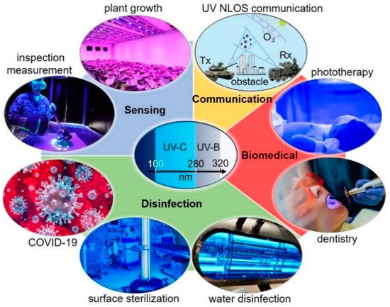
The development of electrically pumped semiconductor diode lasers emitting at the ultraviolet (UV)-B and -C spectral bands has been an active area of research over the past several years, motivated by a wide range of emerging applications. III-Nitride materials and their alloys, in particular AlGaN, are the material of choice for the development of this ultrashort-wavelength laser technology. Despite significant progress in AlGaN-based light-emitting diodes (LEDs), the technological advancement and innovation in diode lasers at these spectral bands is lagging due to several technical challenges.
- AlGaN
- electrically-pumped
- UV-B and -C
- p-doping
- thin films
- nanowires
- hole injection
- quantum wells
1. Introduction
2. Overview of Recent Progress of AlGaN Ultraviolet (UV)-B and -C Lasers
| Reference | Growth Method | Material Type | Lasing Wavelength (nm) | Threshold (kA/cm2) | Substrate | Operating Temp. |
Operating Mode |
|---|---|---|---|---|---|---|---|
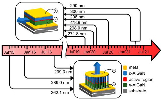
| Zhang et al., 2019 [30] | MOCVD | Thin film | 271.8 | 25 | AlN single crystal | RT | Pulse |
| Sato et al., 2020 [31] | MOCVD | Thin film | 298 | 41 | AlN/sapphire | RT | Pulse |
| Sakai et al., 2020 [33] | MOCVD | Thin film | 278.9 | 19.6 | AlN single crystal | RT | Pulse |
| Omori et al., 2020 [32] | MOCVD | Thin film | 298 | 25 | AlN/sapphire | RT | Pulse |
| Kushimoto et al., 2021 [34] | MOCVD | Thin film | 271.2 | AlN single crystal | RT | Pulse | |
| Tanaka et al., 2021 [35] | MOCVD | Thin film | 300 | 13.3 | AlN/sapphire | RT | Pulse |
| Tanaka et al., 2021 [36] | MOCVD | Thin film | 290 | 35 | AlN/sapphire | RT | Pulse |
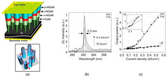
| Zhao et al., 2015 [28] | MBE | Nanowire | 262.1 | 0.2 | Si | 77K | CW |
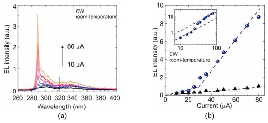
| Zhao et al., 2015 [27] | MBE | Nanowire | 289 | 0.3 | Si | RT | CW |
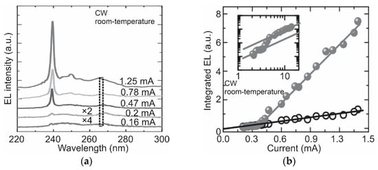
| Zhao et al., 2016 [29] | MBE | Nanowire | 239 | Si | RT | CW |
3. Challenges of AlGaN UV-B/C Lasers
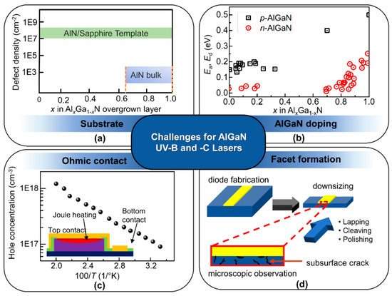
3.1. Substrates and Defects
3.2. P- and N-Doping for High-Al
3.3. Low-Resistive Ohmic Contact
3.4. Facet Formation
4. Critical Technical Areas for AlGaN UV-B and -C Lasers
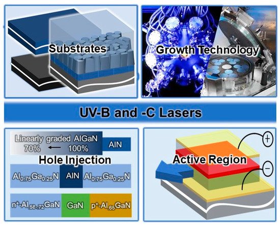
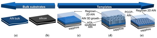
4.1. Substrate Materials
Figure 5 schematically shows all the possible substrates that are used for implementing EP AlGaN lasers.
4.2. Growth Technology
The two most popular methods available for epitaxial growth AlGaN UV laser materials are molecular beam epitaxy (MBE) [128,131,132,133] and metalorganic chemical vapor deposition (MOCVD) [134,135,136]. When it comes to templated substrates, MOCVD is superior to MBE for growing high-quality AlN templates due to high growth-temperatures and -rates [137,138,139].
Although not as extensive as MOCVD, MBE-grown UV materials, i.e., both thin film and NWs, have also been studied over the years. As a matter of fact, MBE offers some distinct benefits over MOCVD in terms of interface diffusion, defect control, memory effect, high hole concentration in p-AlGaN, Mg passivation and significant control over defect incorporation [143]. Due to its relatively low growth temperature MBE grown samples do not suffer from surface damage due to chemical reaction at high temperature often associated with MOCVD. This suggests the superiority of MBE over MOCVD in terms of growing high-quality active regions.
Lasers with buried TJ may require a hybrid MOCVD/MBE growth approach [147,148]. In such structures, a base structure, containing all the layers up to an active region and the p+-side of the TJ, is grown by MOCVD, and the remainder of the device including the n+-side of TJs, n-cladding and n+-contact layers can be overgrown during the second epitaxial growth by MBE. Hence, the hybrid approach, comprising a MOCVD-grown base structure with the active region and MBE-grown TJs, is another viable alternative towards obtaining high-performance UV-B and -C lasers.
4.3. Three Major Techniques for Hole Injection
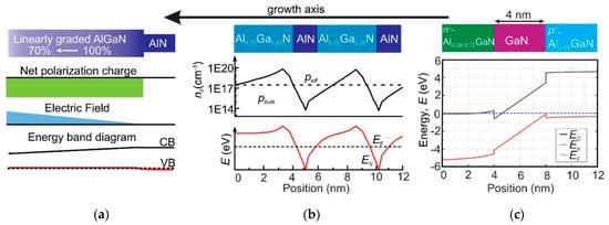
4.3.1. Distributed Polarization Doping
Introducing dopants in AlGaN by compositionally grading, commonly addressed as DPD takes advantage of both spontaneous and piezoelectric polarization. Since its first demonstration, DPD has been widely popular as an effective means to enhance p-AlGaN doping [153].Figure 6a shows how compositionally graded AlGaN creates polarization-induced 3D charges that result in free carriers.
4.3.2. Short-Period Superlattice
A short-period superlattice, comprising of alternate layers of AlxGa1−xN with high and low x doped with Mg (AlxGa1−xN/AlyGa1−yN with x > y) was used to improve hole activation with the help of band offset and strong built-in spontaneous and piezoelectric polarization fields instead of thermal energy [158,159,160,161]. By improving vertical conductivity, the resistance of an SPSL reduced nearly 12 times compared to a bulk layer with the same composition, making the SPSL layer suitable to operate at a high voltage [56].
4.3.3. Tunnel Junctions (TJs)
With the help of polarization doping, successful demonstration of GaN-based TJ was reported since 2001 [162] and in 2016 the first AlGaN based TJ was reported [163]. While p-AlGaN is necessary for p-side cladding, implementing a TJ eliminates the thick p-cladding layer requirement. The use of TJs as an intracavity contact for hole injection through interband tunneling is reported in a number of experimental studies [55,150,151,164,165].
4.4. Active Region
For the successful design and demonstrations of UV-B and -C lasers, one primarily requires a good AlGaN-based active region to obtain high material gain [22,53,154]. This includes not only a good material quality with low-defects and sharp interfaces but also an optimal number of QWs, and the right thicknesses of QWs and barrier with optimal band offsets and adjusting the waveguide thickness [16,167,168]. These considerations will be added by the polarization switching phenomena of emitted light for the unique AlGaN material system [169,170]. Using a higher number of QWs appears to be non-conventional in the wavelengths of interest due to the constraint of uniform pumping of all the QWs with carriers to obtain material gain. If one of the quantum wells cannot be pumped enough, they will operate as a band-edge absorbing layer and then it fails to lase.
5. Demonstration of AlGaN Lasers
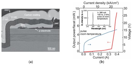
5.1. Thin Film Lasers
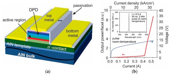
In 2019, the first thin film-based EP AlGaN laser at UV-C was achieved by researchers at Nagoya University, Japan, in cooperation with Asahi Kasei Corporation, Chiyoda City, Japan and Crystal IS, Inc., Green Island, NY, USA [30]. The laser materials were pseudomorphically grown on (0001) bulk AlN substrates by MOCVD. The devices used a single AlGaN 9-nm-thick QW to emit at 271.8 nm. For hole injection, pseudomorphic DPD layers were used on top of p-waveguide. Figure 7a schematically shows the fully processed FP lasers.
5.2. Nanowire Lasers
This entry is adapted from the peer-reviewed paper 10.3390/photonics8070267