Epitaxial graphene on SiC as a hosting substrate for other materials growth is due to its enhanced reactivity compared to chemically inert free-standing exfoliated graphene. Indeed, numerous experimental results by theoretical predictions indicate that by virtue of its physical and structural properties, epitaxial graphene may contain several different highly reactive regions (step edges, charge-unbalanced electron-hole puddles, strained regions, and edges of bilayer inclusions) that may serve as effective nucleation centres.
- epitaxial graphene
- SiC
- deposition
- metals
- insulators
- growth mechanism
1. Introduction
The achievement of large area homogeneous monolayer graphene epitaxially grown on the Si face of SiC (0001) It has been demonstrated that epitaxial graphene on SiC, because of its unique structure, distinct from that of other graphene family representatives [8,9,10], is a promising material to design the next-generation quantum resistance standard of high precision, which make it possible to calibrate mass. Notably, the above-listed examples of sensing applications concern only unmodified pristine epitaxial graphene. At the same time, there is a great deal of interest in epitaxial graphene sensitivity improvement by chemical functionalization [28,29], defect engineering [30,31], and metal oxide nanoparticle decoration [32,33,34].
Applicability and functionality of epitaxial graphene are attributable, in the first instance, to its transfer-free growth on a native substrate through the Si sublimation process during high-temperature annealing of the SiC substrate in an argon atmosphere. The presence of contact between the substrate and graphene is mainly responsible for the observedn-doping and compression of the topmost graphene layer [35,36,37], which is, however, beneficial to promotion of higher reactivity of epitaxial graphene compared to exfoliated counterpart. Indeed, the compressive strain can significantly influence the adsorption capability of graphene with respect to environmental species and individual atoms/molecules [38,39], while electron doping is regarded as a viable means to increase the reactivity toward oxygen [40]. This creates good prerequisites not only for boosting innovative sensing and catalytic applications but also for the exploitation of epitaxial graphene as a substrate for the growth of other functional materials, such as extremely thin metal layers and nanoparticles, semiconducting films, and insulators with good adhesion.
Although the fundamental properties of epitaxial graphene and physics behind epitaxial-graphene-based devices are well documented in the scientific literature, further progress in implementing epitaxial graphene into realistic applications requires both rethinking of the existing knowledge in this field and systematization of new experimental and theoretical results.
2. Key Properties of Epitaxial Graphene as a Substrate for Materials Deposition
Before delving into the discussion of issues related to deposition of metals and insulators on epitaxial graphene on 4H-SiC, we would like first to recall the peculiar properties of epitaxial graphene that make it appealing to the growth of diverse functional materials. For all cases of the materials growth, which will be considered at a later stage, the common feature is that we used the same type of substrate: monolayer epitaxial graphene (MLG) prepared by high-temperature (~1900 °C) thermal decomposition of the Si-face of nominally on-axis 4H-SiC (0001) substrates in Ar atmosphere [41]. The graphene formation process encompasses three successive stages: (i) initial Si sublimation that takes place in inductively heated graphite enclosure in highly controlled conditions (gas, pressure, time), (ii) C-rich 6√3 × 6√3
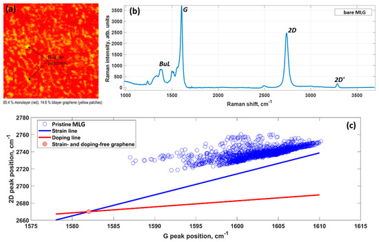
MLG quality control is carried by two independent methods: optical reflectance mapping [43] and micro-Raman spectroscopy. Typically, the grown samples are composed of 85% monolayer graphene (and even larger % for recently synthesized samples) and 15% bilayer graphene that is represented by small bilayer patches above the first graphene layer (Figure 2a). The presence of randomly distributed bi-layer graphene islands within MLG sample can be beneficial to provide extra nucleation sites during early growth stages. More information about the intrinsic properties of the epitaxial graphene on SiC can be extracted from the analysis of the Raman mapping data [42].
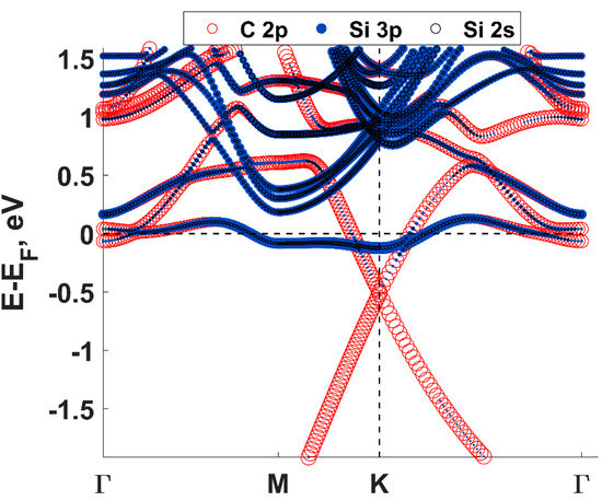
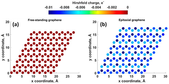
Density functional theory (DFT) calculations showed that the charge transfer between SiC and graphene caused the shift of the Dirac cone (0.49 eV) below the Fermi level EF (Figure 3), thereby corroborating experimental findings on SiC-substrate-inducedn-type doping of graphene. In this regard, a comparison of the charge redistribution map of free-standing graphene with that of epitaxial graphene revealed a pronounced accumulation of negative charge on SiC-supported graphene sheet (Figure 4). [44], there is a direct correlation between the electron density of graphene and the adsorption energy of water molecule. Indeed, the better wettability of graphene by water, the larger number of nuclei for Al2O3formation.
The analysis of Figure 2c also indicates that as-grown epitaxial graphene samples were under compressive strain. This is contrary to the results of theoretical calculations, according to which graphene on SiC would undergo a lattice expansion rather than compression. This is because the lattice constant of graphene is smaller than that of SiC. This discrepancy can be explained by the fact that graphene on SiC is forced to compensate for the mismatch in their coefficients of thermal expansions through building up compressive stress after cooling down to room temperature [45].
While the adsorption capability of expanded graphene originates from the formation of localized dangling-bond states that can promote strong binding with environmental adsorbates [46], the mechanism behind the interaction between compressively strained graphene and environmental species is not so obvious. On the one hand, a shrinkage of graphene (C-C bond length shortening) may induce delocalization of electron wavefunction over the planar graphene structure and decrease the density of dangling bond states, which are available for surface reactions [46]. On the other hand, the compressive strain can cause the formation of nano-ripples, which are able to adsorb atomic species at ridge sites [38].
Further, we highlight four most probable highly reactive regions on epitaxial graphene/SiC, which may serve as native seeds for the growth of external materials: (a)Step edges. The supporting SiC substrate is responsible not only for the doping of graphene but also for the appearance of charge density fluctuations. Compressive or tensile strain leading to alteration of orbital hybridization and substrate-induced strain fluctuations are considered as another important factor determining an increased reactivity of epitaxial graphene compared to exfoliated graphene.(d)Edges of the bilayer graphene inclusions. Since as-grown monolayer epitaxial graphene usually includes nanoscale overgrown areas related to bilayer graphene, it is reasonable to assume that unsaturated edges of these inclusions may create extra nucleation sites.
3. Deposition of Noble Metals on Epitaxial Graphene/4H-SiC by dc Magnetron Sputtering
The behavior of noble metals on epitaxial graphene is a matter of considerable interest, as its deep understanding may boost the development of new sensor designs based on nano-plasmonics. Our recent findings shed light on the interplay between two selected magnetron-sputtered noble metals (silver and gold as representatives of metals with best plasmonic activity) and epitaxial graphene on 4H-SiC [43,47,48,49]. From the theoretical point of view, both considered metals interact with epitaxial graphene through weak van der Waals forces, which is confirmed by a low adsorption energy that is below the lower limit of chemisorption and small charge transfer from metals to graphene [49]. Concomitantly, silver atoms interact stronger with graphene surfaces compared to gold species.
Furthermore, the predicted cohesive energy of bulk gold has a more negative value (−3.62 eV) as compared to the cohesive energy of bulk silver (−2.95 eV), suggesting that the Au-Au interaction is more stable and stronger than the Ag-Ag interaction. This difference provides an additional driving force for the MLG-assisted self-assembly of just adsorbed gold into interconnected nanostructures. It is interesting to note that the difference in the interaction strength characteristically manifests itself in Raman spectra of epitaxial graphene Particularly, the Raman spectrum of pristine epitaxial graphene remains typically intact after gold deposition (except for small displacements of the main characteristicGand 2Dpeaks), while silver deposition causes substantial changes in Raman activity reflected in an appearance of defect-related Raman peaks (D,D’,D+D’,D+G, andD**) and huge red-shift of the 2Dpeak.
The effect of magnetron-sputtered Ag film thickness on the morphological evolution during film growth and phonon properties of epitaxial graphene has been thoroughly investigated in [47,48]. As can be seen from Figure 9, only 2 nm-Ag film exhibits island-like morphology with isolated circular islands.
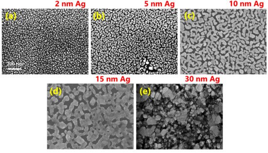
Further increase in the nominal thickness of Ag initially led to the appearance of elongated islands (Figure 9b), followed by the formation of an interconnected network (Figure 9c,d) and a continuous silver layer at a thickness of 30 nm (Figure 9e).
Careful analysis of defect-related Raman modes of epitaxial graphene after silver deposition enabled the estimation of the density of generated defects and elucidate their nature [47]. It was revealed that theD/Gintensity ratio is very sensitive to alternation of the silver thickness (Figure 10a–d), demonstrating obvious enhancement with increasing of Ag-layer thickness.
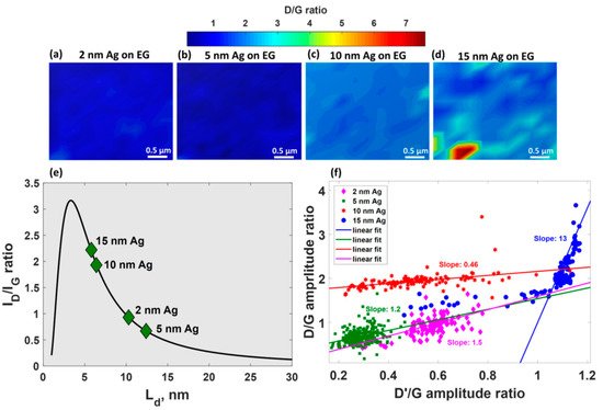
Such behaviour implies two important consequences: (i) reduction in domain size in graphene (Figure 10e) and (ii) increase in density of defects up to 9.5 × 1011cm−2for 15 nm-Ag-decorated epitaxial graphene. The peculiar dependences ofD/Gamplitude ratio onD’/Gamplitude ratio (Figure 10f) for all considered films suggest that the boundary-related defects are preferential defects in the MLG decorated with 2–10 nm Ag films whilesp3-type defects dominate in the case of 15 nm-Ag-covered MLG.
It was also shown that the magnetron-sputtered 2 nm- and 5 nm-Ag layers donate electrons to epitaxial graphene, giving rise to a large area uniformn-doping of epitaxial graphene (0.95–1.36 × 1013cm−2) [48], which is manifested by huge red-shift of 2Dpeak and a very narrow spread of experimental data points in 2D–Gspace. Concomitantly, the deposition of thicker Ag films (10 and 15 nm) caused large strain and doping fluctuations.
4. Atomic Layer Deposition of Insulators on Epitaxial Graphene
Apart from the growth of pure metals on epitaxial graphene, the development of controllable and reliable synthesis technology of high-kdielectrics (for example, Al2O3) is of paramount practical importance. It is due to the multifaceted role they play in graphene-based devices as gate insulators in field-effect transistors, tunneling barriers, and protective layers [55,56,57,58]. In this context, the integration of epitaxial graphene with insulators can bring this material closer to real electronic applications. It was revealed that for a deposition temperature of 250 °C, the transition from island-based growth to layer-by-layer growth mode occurs after 40 ALD cycles that correspond to ~2.4 nm (Figure 13).
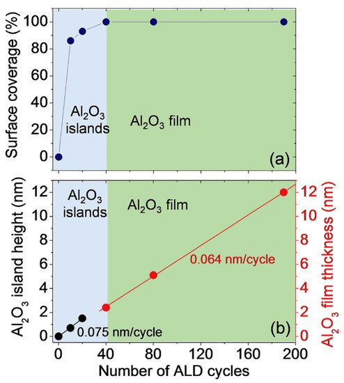
Such a fast transition of the growth mode can be interpreted by the existence of a high density of nucleation centers on the epitaxial graphene surface during early growth stages, which is uncommon for other types of graphene, especially for free-standing exfoliated graphene. This experimental finding is reinforced by the current maps (at a bias Vtip= 1 V) measured by conductive-atomic force microscopy (C-AFM) on epitaxial graphene before and after deposition of Al2O3. Obviously, epitaxial graphene on 4H-SiC makes it possible to form highly uniform Al2O3thin films without pre-functionalization or seed layers [44]. Such an effect can be ascribed to higher reactivity of monolayer graphene than that of bilayer or multilayer graphene.
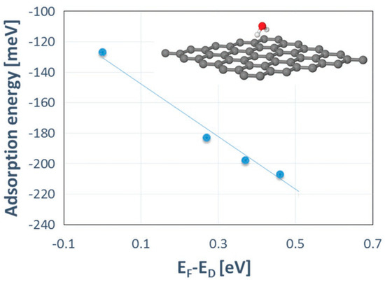
Additional theoretical work has been performed to fully understand the growth mechanism of Al2O3on epitaxial graphene [44]. The initial idea was to link the adsorption energies of the precursor molecules (trimethyl aluminium, TMA, and water, H2O) and graphene doping levels. However, no sufficient credible evidence to prove that TMA adsorption depends on the Fermi level position in graphene was provided.
On the other hand, the adsorption energy of water is more sensitive to the doping of graphene and was found to increase with increasing the negative charge on graphene (Figure 5). The stronger the adsorption, the shorter the diffusion path of water molecules. Such locally trapped water molecules may then act as effective reactive sites during subsequent TMA pulses.
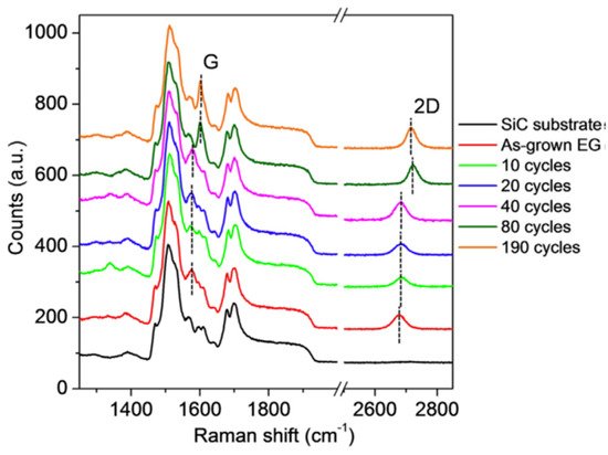
Further experiments by using Raman spectroscopy have shown that the ALD process does not cause structural damage of epitaxial graphene, which is evidenced by the absence of defect-related Raman peaks for all investigated samples (Figure 15). The substantial changes related to the blue shift of the 2D peak started to appear only after 80 ALD cycles, and that epitaxial graphene experiences a large compressive strain due to the formation of the continuous film.
This entry is adapted from the peer-reviewed paper 10.3390/app11135784