Barrier Layer of Cu Interconnects: History
Please note this is an old version of this entry, which may differ significantly from the current revision.
Contributor:

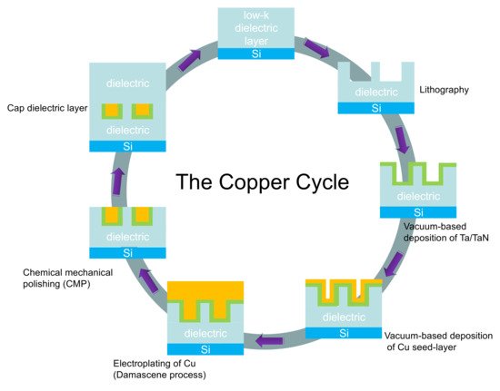
The barrier layer in Cu technology is essential to prevent Cu from diffusing into the dielectric layer at high temperatures; therefore, it must have a high stability and good adhesion to both Cu and the dielectric layer. In the past three decades, tantalum/tantalum nitride (Ta/TaN) has been widely used as an inter-layer to separate the dielectric layer and the Cu. However, to fulfill the demand for continuous down-scaling of the Cu technology node, traditional materials and technical processes are being challenged. Direct electrochemical deposition of Cu on top of Ta/TaN is not realistic, due to its high resistivity. Therefore, pre-deposition of a Cu seed layer by physical vapor deposition (PVD) or chemical vapor deposition (CVD) is necessary, but the non-uniformity of the Cu seed layer has a devastating effect on the defect-free fill of modern sub-20 or even sub-10 nm Cu technology nodes. New Cu diffusion barrier materials having ultra-thin size, high resistivity and stability are needed for the successful super-fill of trenches at the nanometer scale. In this review, we briefly summarize recent advances in the development of Cu diffusion-proof materials, including metals, metal alloys, self-assembled molecular layers (SAMs), two-dimensional (2D) materials and high-entropy alloys (HEAs). Also, challenges are highlighted and future research directions are suggested.

  • Cu diffusion barrier
  • platinum group metals
  • 2D materials
  • self-assembled monolayers

1. Introduction

Ever since the development of the integrated circuit (IC) about 60 years ago, aluminum (Al) and silicon dioxide (SiO2) have been most widely used as conductor and insulator materials for the fabrication of micro-processors [1,2]. As technical demands grew, the continuous decrease of the feature sizes and the explosive increase of the number of transistors in micro-processors resulted in the growth of so-called gate delays [3,4]. To solve this issue, new wiring materials with resistivity lower than Al and dielectric materials with dielectric constant (so-called low-κ) lower than conventional SiO2 have to be used as alternatives. IBM announced in 1997 the replacement of Al with copper (Cu) as the interconnect material in semiconductor processing [5]. As compared to Al, Cu has a smaller gate delay due to its lower electrical resistivity, but higher electro-migration, stress-migration resistances and melting point [6]. However, a big problem of switching Al to Cu is that the conventional methods used for Al deposition (sputter deposition) and patterning (reactive ion etching) are not suitable for Cu, as Cu is corroded during standard chip manufacturing processes. Therefore, the fabrication technique has to be upgraded for Cu patterning and deposition.
The structure of Cu interconnects is usually patterned by a so-called damascene process [7,8], in which the dielectric layer is patterned in advance, followed by the sequential deposition of a diffusion barrier layer and the filling of the patterned trenches with Cu. The excess of Cu can be removed by a chemical mechanical polishing (CMP) process. Among the many deposition methods of Cu, the electrochemical deposition (ED) technique [9,10] has been proven to be the most economic and efficient way to super-fill damascene features without defects, as compared to techniques such as electroless plating, vacuum-based physical vapor deposition (PVD) and chemical vapor deposition (CVD). The atomic layer deposition (ALD) method is another way to generate uniform Cu thin film. Based on sequential layer-by-layer deposition and self-limiting behavior, ALD provides high conformity of thin film quality and accurate control of layer thickness, in spite of the slow deposition rate and low throughput. Inspired by this method, electrochemical atomic layer-by-layer deposition (known as e-ALD) has been developed to fabricate ultra-thin Cu film, including two main steps: (1) deposit a sacrificial atomic layer of an appropriate metal by holding an electrode potential within the underpotential deposition region; (2) release the electrode potential to induce the spontaneous displacement of sacrificial metal layer by atomic Cu layer [11]. However, the introduction of copper as interconnects also raises some other challenges, including the degradation of devices due to the diffusion of Cu into the Si and Si-based insulating layers at rather low temperatures [12], the absence of a self-passivized oxide layer causing the corrosion of Cu under chip fabrication process, as well as the poor adhesion between Cu and insulating layers.
To solve these problems, a suitable barrier material with good adhesion to Cu is required to prevent Cu from diffusing into the dielectric layer. The qualified diffusion barrier materials need to be refractory and inactive to both conductors and insulators at rather high temperatures, normally including transition metals such as tantalum (Ta) [13,14,15], tungsten (W) [16,17,18], titanium (Ti) [19,20] and their composites with nitrogen (N), carbon (C) or Si, such as Ta/TaN [21,22,23,24,25], W2N [26,27,28], TiN [29,30,31,32], TiC [33,34,35], TaSiN [36,37,38], Si3N4 [39] and so on. As those state-of-the-art barrier materials are typically poorly conductive, pre-deposition of a Cu seed layer is often needed for the electroplating of Cu, but the Cu seed layer is prone to dissolution in an acidic electrolyte in the subsequent ED process, making it hard to obtain a uniform Cu layer. However, direct plating of uniform Cu film on diffusion barrier materials is of crucial importance in the modern fabrication process. This review briefly summaries the latest development in Cu barrier materials, including state-of-art Ta/TaN, platinum group metals (PGMs) such as ruthenium (Ru)-based materials, 2D materials, self-assembled molecular layers (SAMs) and high-entropy alloys (HEAs). Some of those new barrier materials provide not only reliable Cu diffusion barrier properties during thermal annealing, but also anti-corrosion of Cu in the electrolyte. High-quality ultra-thin film of CVD graphene [40], hexagonal boron nitride (h-BN) [41], magnetron sputtering HEAs [42] and dip-coated SAMs [43] have shown great ability to prevent metals from corrosion in salty solution. In addition, some metal oxide layers (e.g., Ru oxide [44] and Ir oxide [45]) have also been proven as reliable metal corrosion resistants.

2. Cu Interconnects and Diffusion Barrier Materials

Cu interconnects function as internal wiring, connect each circuit compartment and distribute power. In the damascene process, the Cu wiring technique can be vividly demonstrated by the so-called Cu cycle [46] depicted in Figure 1, which combines a series of individual processing steps to fabricate a single level of Cu interconnect architecture on a Si wafer.
Figure 1. Schematic demonstration of the Cu cycle.
Typically, the Cu cycle starts from the deposition of a low-κ dielectric layer on the Si wafer. Afterwards, the dielectric film is patterned by lithographic method. Then a thin film of Ta/TaN diffusion barrier layer is deposited on top of the dielectric pattern by means of PVD or CVD. Due to the low conductivity and poor nucleation behavior of Cu on the Ta/TaN layer, vacuum deposition of Cu seed-layer is needed to ensure that the following ED process of Cu is able to superfill the damascene features. Finally, a CMP process is conducted to remove the over-plated Cu. The Cu cycle restarts with the deposition of another dielectric layer. During the whole cycle, the defect-free filling of Cu in the damascene trenches is crucial.
However, according to Moore’s law [47], the number of transistors in a chip doubles every two years, that is, next generation devices demand the continuous decrease of feature sizes, which as a consequence increases the difficulty of defect-free filling of the trenches in the damascene process. It is well known that the resistances of conventional diffusion barrier materials are too high to be the substrate for direct ED of Cu [48,49,50,51], and an unpleasant phenomenon called “terminal effect” often appears [11,52,53,54,55,56,57,58,59]. This effect becomes more pronounced with the transition from 200 to 300 mm Si wafer. Normally the electrical contact is placed at the periphery of the wafer. When the ED of Cu is performed on a resistive substrate, there is a dramatic IR drop (potential gradient) across the wafer from the contact point to the wafer center, resulting in the non-uniform distribution of current over the resistive substrate with inhomogeneous Cu ED deposition. For this reason, an extra Cu seed layer has to be deposited in advance via PVD [60,61,62,63], CVD [64,65,66,67,68,69], ALD [70,71,72,73] or electroless methods [74,75,76,77,78]. The seed layer prepared by some methods such as PVD or electroless deposition normally causes undesired “over-hang” at the trench opening, which becomes devastating within the sub-45 nm region and results in unsuccessful filling in the following Cu ED process, as illustrated in Figure 2 [79].
Figure 2. Schematic illustration of the “over-hang” formed by electroless deposition of Cu seed layer, leading to the voids formed by the subsequent electrochemical Cu deposition during a damascene process. (a) The formation of Cu overhanging clusters via electroless deposition; (b) growth of Cu overhanging clusters during electrochemical Cu deposition; (c) failure of Cu super-filling of damascene feature. Reproduced from Hong et al. [79]. Copyright 2005 Elsevier Ltd. All rights reserved.
To avoid this, new barrier materials and techniques must be developed. Desirable characteristics for ideal diffusion barrier materials have been proposed [80,81], including (1) excellent adhesion to Cu metal and dielectric layer; (2) immiscibility with Cu and an ability to prevent Cu diffusion at high temperatures; (3) good conductivity for direct ED of Cu; and (4) simplicity of uniform deposition of ultra-thin film on dielectric layer. In order to find a suitable replacement of traditional barrier materials, attention has been paid to PGM-based materials (e.g., Ru [82,83,84,85], iridium Ir [86,87,88,89], palladium Pd [90] and their composites with other materials [91,92,93,94,95,96,97]), 2D materials (e.g., graphene [98,99], hexagonal boron nitride h-BN [100], and molybdenum disulfide MoS2 [101,102]), SAMs [103,104,105,106,107] and HEAs [108,109,110,111]. The comparison of properties between new barrier materials and traditional Ta/TaN is listed in Table 1. Compared to Ta/TaN, PGMs (e.g., Ru and Ir) and 2D materials (e.g., graphene) have lower electrical resistivity and comparable melting point. The SAMs’ electrical resistivity and melting point strongly depend on their molecular nature, while HEAs have a poor electrical resistivity and their melting point is normally over 1000 °C. SAMs have the easiest deposition method by immersing substrate into the solution containing appropriate molecules. Concerning the layer thickness, 2D materials hold great potential for size downscaling, as single-layer graphene is only one-atom thick.
Table 1. Brief comparison of properties, fabrication methods and expected thickness of barriers.

3. Platinum Group Metals (PGM)-Based Materials

Among PGM metals, Ru receives the most attention. It is an air-stable metal with a much lower electrical resistivity (ρRu = 7.1 μΩ·cm) [83] compared to that of Ta (ρTa= 13 μΩ·cm), which allows the direct electrochemical plating of Cu. More importantly, Ru has a melting point as high as 2334 °C [112], shows negligible solubility [113,114,115] but fantastic wettability with Cu and exhibits excellent adhesion to electroplated Cu at elevated temperatures [82,83,84,85]. Therefore, Ru has been considered as a promising candidate to replace the traditional diffusion barrier materials. Thin films of a Ru barrier layer can be placed on solid substrate via gas phase deposition methods such as PVD, CVD and ALD, or wet deposition methods such as ED and electroless plating. Chyan et al. [84] showed a successful example of the direct ED of a conformal Cu coating layer with controllable thickness on polycrystalline Ru electrode. Annealing up to 600 °C caused no apparent dewetting at the Cu/Ru interface, and more importantly, there was no new phase formed upon further annealing at 800 °C. Chan et al. [85] demonstrated that a high-quality thin film of Cu layer can be formed on top of a 20 nm thin film of Ru deposited on a Si wafer via a standard magnetron sputtering system, showing a Cu ED efficiency as high as 95%. The 20 nm Ru film was sufficient to prevent Cu from diffusing into Si upon annealing at 450 °C for 10 min, but the delamination of Ru thin film from a Si wafer can be seen at 550 °C, resulting in the penetration of Cu into Si substrate. However, reduction of the thickness of Ru layer leads to a decrease in both the Cu ED efficiency and the Cu diffusion-proof temperature. Arunagiri et al. [83] showed that even though a Ru thin film with reduced thickness of 5 nm was able to arrest the diffusion of Cu into Si after annealing at 300 °C for 10 min, only a Cu ED efficiency around 90% was obtained, and a new ruthenium silicide phase was formed at the temperature of 450 °C. Accordingly, a failure mechanism of Cu/Ru/Si system (Figure 3) was proposed by Damayanti et al. [116]. They suggested that the failure appeared at high annealing temperatures and was initiated by the formation of polycrystalline ruthenium silicide, further promoting the diffusion of Cu into Si substrates with the formation of copper silicide protrusions.
Figure 3. Schematic description of the barrier failure mechanism in Cu/Ru/Si system. (a) Intact Ru barrier at the initial stage, (b) barrier failure induced by the formation of ruthenium silicide, (c) complete dissolution of metallic Ru to form ruthenium silicide, and (d) Cu diffusion through ruthenium silicide to form copper silicide.

This entry is adapted from the peer-reviewed paper 10.3390/ma13215049

This entry is offline, you can click here to edit this entry!