LIFT is a printing method that allows material deposition in a tiny quantity, resulting in a solid or liquid pixel with high resolution. For the very first time, Bohandy et al. [
12] developed and explained this technique. Since then, various techniques based on LIFT have been established for multiple materials printings used in specific applications.
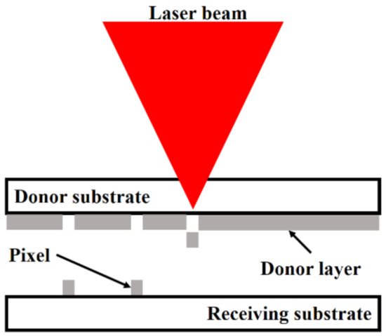
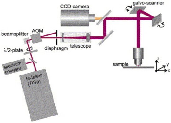
Figure 1 presents a schematic of the processes involved in the LIFT technique [
13,
14,
15]. As presented in
Figure 1, the solid-phase pixels are transferred after irradiating the thin layer or film (donor) via a laser-pulse, made up of an engrossing material placed on a translucent substrate. As the layer’s irradiation occurs, the light to matter encounter happens at the periphery, generating a stout pressure locally. Due to this phenomenon, a minor portion of the donor film (pixel) is evicted and accumulated on the receiving substrate, located close to the donor [
16].
LIFT is a single action DLW technique, which can deposit the localized micro-patterns of almost every material. Sensitive materials can be printed without changing their properties. This also allows direct printing of multilayers in a solvent-free atmosphere, deprived of requiring any sort of shadow mask or vacuum system [
35,
36]. This method has recently become famous as an alternative method to manufacture electronic components [
37], organic transistors [
38,
39,
40], organic diodes for light-emitting [
41,
42,
43], micro-electro-mechanical systems [
44,
45], sensing devices [
46,
47,
48,
49], and biological tissue [
50,
51]. LIFT has a few pros and cons. For this purpose, the efficient expansion of a laser printing method necessitates a comprehensive understanding of the physio-chemical phenomenon causing the material’s ejection and accumulation.
2.2. LIFT: Flyer Velocity and Shock-Wave Formation
The transfer of pixels is usually encouraged by mechanical forces due to laser beam energy absorption at the boundary of the translucent donor (substrate) and receiver (film). A rapid upsurge in temperature intensity and pressure happens within the limited volume, which disintegrates the donor around the irradiated region, thus pushing the pixel away to the receiver. Besides this, a shock-wave is generated, spreading in the pixel-front.
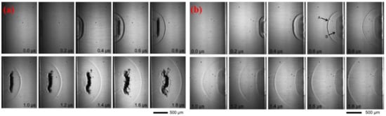
Figure 2a shows the images captured, in the case of triazene-polymer (=460 nm), irradiated with a laser having fluence equal to 110 mJ·cm
−2. The images were captured after rotating the sample up to 180° to have a clear front view of ablation, as shown in
Figure 2b [
57]. A noticeable shock-wave with the same profile and extension characteristics can be analyzed. The primary difference is the product front’s replacement with an opaque entity evicted from the substrate such that the flyer becomes noticeable after 0.4 ms irradiation time. Initially, the flyer has a precise flat shape consistent with the ablated spot. Later on, it enlarges, becomes inaccurate, and loses its original profile. The flyer existence shows that a single laser pulse does not ablate the entire triazene layer at the selected fluence. The flyer contains an undecomposed polymer, evicted by the thrust pressure made throughout ablation and breakdown of the beneath part.
Figure 2. (
a) Backside images captured for 460 nm triazene-polymer ablation at laser fluence equal to 110 mJ·cm
−2, and (
b) front view ablation of 460 nm triazene-polymer ablation at laser fluence equal to 110 mJ·cm
−2. In both images, laser is at the left-side, and the substrate is placed at right-side [
57]; with permission from Elsevier.
The pixels’ ejection velocity is determined from the shadowgraph’s analyses, which primarily depends on laser beam fluence and donor thermo-physical characteristics. When the pulse duration is in the range of a picoseconds~microseconds, no substantial alteration in velocity is identified. The solid pixels are usually expelled with velocities in the range of 200–1200 ms
−1. Besides, it is also probable to emit pixels at a very small velocity equal to 34 ms
−1, resulting in no shock-waves formation. Such conditions were tested while transferring lead zirconate titanate (PZT) using a laser of 100 fs [
58]. Apart from the laser energy captivated by the substance to heat the substrate, another portion is utilized to fracture the substrate and moved away to the receiver. For the LIFT process, the perfect conditions are defined as:
- (a)
-
Bound heat-diffusion within the substrate to dodge the impairment and to generate the molten fragments.
- (b)
-
A significant portion of laser energy used to fracture the substrate and hold the pixel speed for a short time interval to confirm the pixel’s flat arrival at the receiver.
- (c)
-
In the case of particular materials, the femto-second (fs)-laser permits the regulation of this energy distribution.
In the solid phase, the generation of shock-wave is the principal disadvantage of LIFT. Fardel et al. [
59] confirmed that, when it arrives at the donor, back-scattered, an interaction occurs between the reflected shock-wave and pixel. This interaction stops the pixel motion and causes pixel’s de-shape. Using a gap of a few micrometers between the donor and receiver, laser printing can be achieved at atmospheric pressure. Various printing experiments were performed under vacuum to exclude this shockwave, but the flyer broke due to its very high velocity when arriving at the substrate [
59]. Therefore, a compromise has to be made between the intensity of shock-wave formation and the pixel’s velocity by controlling the gas pressure and laser beam fluence [
60]. Usually, the working pressure is within the range of 10–100 mbar, allowing the pixels’ safe travel with a gap of less than 50 mm. This process involves the mechanical force formation that breaks the donor. So, printing a brittle material or thick layer (>a few micrometers) is a challenging task. There are two methods used to solve this issue. Rapp et al. [
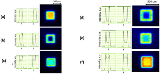
61] utilized a particular laser profile to independently regulate the energy needed to break a film, focused at the beam’s edge. It can be observed in
Figure 3 that, after integrating the two beams having different energies and shapes, the laser fluence can be enhanced at the beam’s edge, while a low fluence value can be obtained in the central beam portion. This technique allows printing polymer films with more than 1 mm thickness without compromising resolution [
62].
Figure 3. Beam profiles with associated intensities along the
x- and
y-directions in the LIFT experimental setup at the donor layer: (
a) a square mask, (
b) with mask at contours, (
c) with a combination of (
a) and (
b) techniques, (
d) high-intensity ratio, (
e) medium intensity ratio, and (
f) low-intensity ratio [
61]; with permission from Elsevier.
2.3. Various Materials Printed by LIFT and Their Properties
Shen et al. [
63] used LIFT to transfer micro-stripes of polyimide, with a thickness of 1.2 µm, with laser fluence of 39 mJ·cm
−2 and 50 pulses. The deposited strip height (20 to 140 nm) increases with an increment in the laser fluence (34–52 mJ·cm
−2).
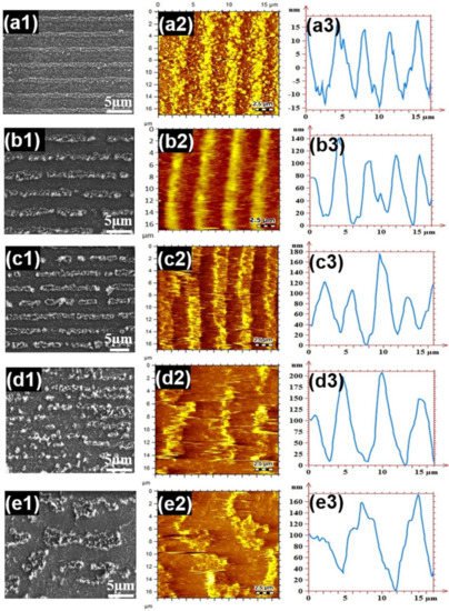
Figure 4a–e show the influence of the laser beam fluence, having nano-second laser pulse, on the polyimide donor-film (thickness ~1.2 µm). The laser fluence was used in the range of 34~51 mJ·cm
−2, while the laser pulses were forty. From
Figure 4(a1–e1), one can observe the scanning electron microscopy (SEM) images of stripes passed on via LIFT. At relatively low fluence (34 mJ·cm
−2), the stripes showed an entire structure with sharp contours, as shown in
Figure 4(a1). On the other hand, the stripes began to break-down at the laser fluence higher than 34 mJ·cm
−2 and balling phenomena can be analyzed clearly in
Figure 4(b1–e1). In
Figure 4(a1–c1), the size of micro-stripe is 3 µm. Besides, the stripes morphologies were examined using atomic-force microscopy (AFM). These results are presented in
Figure 4(a2–e2). The height profiles of the stripes are shown in
Figure 4(a3–e3). One can analyze that an increment in the laser fluence causes non-uniformities in the stripe height.
Figure 4. Laser fluence and stripes morphologies: (
a1–
e1) scanning electron microscopy, (
a2–
e2) atomic force microscopy, and (
a3–
e3) stripes height profiles variations; [
63]; with permission from Elsevier.
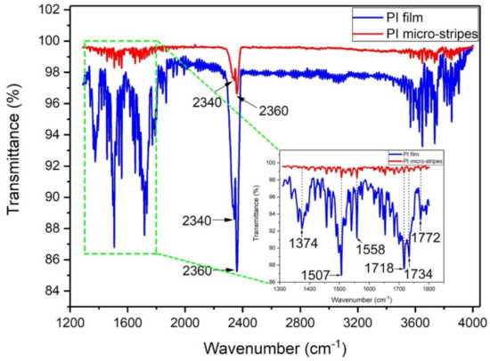
To identify the polyimide stripes composition, Fourier transform infrared spectroscopy (FT-IR) measurement was performed.
Figure 5 displays the results of FT-IR spectra. The results show the spectra of polyimide and stripes generated after LIFT. It is worth mentioning that only a material fraction was ejected from the polyimide-donor film. Hence, the polyimide films absorption intensity was higher than stripes. In
Figure 5, polyimide showed three absorption bands at (a) 1374 cm
−1, (b) 1734 cm
−1, and (c) 1772 cm
−1, which correspond to the chemical bond vibration between Carbon and nitrogen, and carbon and oxygen (symmetric and asymmetric). At 2340 cm
−1 and 2360 cm
−1, the bands are allocated to carbon dioxide captivation, produced during acrylic acid imidization. Finally, the FT-IR spectrum shows that the stripe’ composition remains the same when transferred from polyimide substrate [
63].
Figure 5. Fourier transform infrared spectroscopy of polyimide and stripes formation [
63]; with permission from Elsevier.
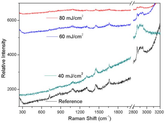
Papavlu et al. [
64] demonstrated the capability of LIFT for the pattering of liposomes at a micro-scale. These patterns are commonly used in biosensors and drug delivery systems. The solution was optimized by using dynamic release layers with various thicknesses. A clean transfer was attained for triazene polymer film having thickness more than 150 nm. Different distinct outlines were obtained with the laser beam fluences in between 40–60 mJ·cm
−2 and 193 nm irradiation. They determined that the distance between target and substrate does not influence the micropatterns morphologies.
Figure 6 shows the Raman spectroscopy of the printed samples. Moreover, Raman spectroscopy for the chemical composition of liposomes remained the same for the laser fluences between 40 and 60 mJ·cm
−2. Liposome arrays were manufactured with the least volume, suggesting that LIFT is a promising practice for liposome patterning.
Figure 6. Liposome Raman spectrum [
64]; with permission from Springer.
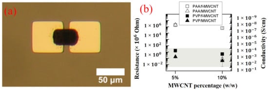
Boutopoulos et al. [
65] suggested that LIFT is an alternate and up-coming method for the composite layers printing of polymers + carbon nanotubes (CNT). LIFT deposited polyvinylpyrrolidone (5%) + functionalized multiwall carbon nanotubes and polyacrylic acid (10%) + functionalized multiwall CNTs layers showed a uniform CNTs distribution within polymer matrices. The composite layers’ electrical characterization was accomplished by accumulating pixels from all the targets onto aluminum micro-electrodes detached by a breach of 10 µm.
Figure 7a shows a precise 30 × 40 µm
2 polyvinylpyrrolidone (5%) + functionalized multiwall CNTs pixel printed on aluminum micro-electrodes using laser fluence of 220 mJ·cm
−2. A Hewlett Pack was used to characterize all the deposited layers.
Figure 7b shows the deposited composite layers’ confrontation and electrical-conduction using direct-current. It can also be analyzed that, for a given composition of polymer and CNTs, composite layers with functionalized multiwall CNTs methodically presented low conduction related to non-functionalized multiwall CNTs. This can be attributed to the functionalized CNT’s primarily feebler electrical characteristics compared to non-functionalized CNTs.
Figure 7. LIFT depositions: (
a) Optical microscopy image of polyvinylpyrrolidone (PVP) + functionalized multiwall carbon nanotubes (f-MWCNT), and (
b) electrical characteristics [
65]; with permission from Applied Physics Letters.
Dinca et al. [
66] presented LIFT depositions for both single- and multiple-pixel depositions. The final goal was to obtain polyethyleneimine (PEI) and polyisobutylene (PIB) continuous pixels on surface acoustic waves (SAW) surfaces. After depositions with multiple fluences, the coated transducers’ responses were measured. They determined that a laser fluence below 625 mJ·cm
−2 was obligatory to stop interdigital transducers impairment for the sensor devices. These measurements show that LIFT can print sensitive polymer pixels onto the transducer devices. Feinaeugle et al. [
67] demonstrated a thermo-electric energy harvesting device’s fabrication via LIFT of intact solid thin films. Thermo-electric materials, including bismuth telluride (Bi
2Te
3), bismuth selenide (Bi
2Se
3), and bismuth antimony telluride (Bi
0.5Sb
1.5Te
3) were printed via an excimer laser (nanosecond pulse) on an elastomeric polydimethylsiloxane coated glass substrate. The generator Seebeck coefficient and series resistance were 0.17 mV·K
−1 and 10 kΩ, respectively. Stewart et al. [
68] used a UV-absorbing triazene polymer (TP) as a DRL layer to propel other materials forward without any damage. A picosecond pulse length was used to irradiate TP-films, which produced considerable deviations in the ablation process compared to the nanosecond pulse ablation. The shorter pulse length declines the ablation threshold and ablation threshold, observed in thinner films less than 100 nm. This propels the shockwave and flyer faster and forms a more disjointed flyer. These effects are due to the picosecond laser’s pulse length timescale, resulting in higher energy ablation products by elevating the TP’s effective absorption. This, in return, reduces losses due to the fast process.
Karnakis et al. [
69] used a KrF excimer laser with wavelength (248 nm) and pulse duration (30 ns). Pyrene-doped PMMA donor film was irradiated to transfer pyrene molecules to poly-butyl-methacrylate (PBMA) substrate. The laser pulse passed through a beam homogenizer to ensure the same energy distribution on the whole area of the laser spot and was focused on a 1.2 cm spot size. Both films were spin-coated on quartz substrates. The donor film had a thickness of 0.1–4 µm thickness, while the receiving polymer was 2 mm thick. It was found that the receiving polymer surface fluorescence spectra will be changed if the molecules decayed or just stuck to the polymer surface. However, the receiver surface reserved its original smoothness. Nakata et al. [
70] examined the LIFT of Rhodamine 610 laser dye on a SiO
2 substrate via Nd: YAG laser (532 nm and 8 ns). Ethanol solution droplets (donor film) were applied on a gold (base film), placed at 15 µm from the SiO
2 substrate. The fluorescence emission was optimal at laser fluence (49 mJ/cm
2) under vacuum condition.
Pentacene (PE) is ideal for replacing amorphous silicon in organic thin-film transistors (TFTs). Blanchet et al. [
40] presented experimental analyses of thin PE-film deposition via Nd-YAG laser (266 nm and 10 ns). The laser beam was collimated onto an area of 3 cm
2 target surface under an ultrahigh vacuum of 10
−7 Torr. The laser-evaporated PE-films’ semiconducting performance was analyzed. It was found comparable with the PE-thin films deposited by thermal evaporation. Polyaniline (POLY) is a unique conducting polymer. Blanchet et al. [
71] carried out a pixelized transfer of POLY + nanotube structures via the thermal imaging technique. An infrared laser (40 W and 780 nm) was engrossed over a thin metallic-layer (donor base) having POLY coating. Light to heat conversion resulted in gaseous products and shockwaves, resulting in the material transfer from the substrate to the receiver. Using this method, the composite’s wide line equal to 500 µm was printed with a 7 µm gap with a 2 S/cm conductivity. Blanchet et al. [
72] printed a TFT backplane having 5000 transistors with 20 µm channel on a substrate (50 × 80 cm
2). Due to the deficiency of built-in registration, the sources and drains were shifted from the gate’s center. The maximum misregistration was less than 200 µm. Electronic systems printed using this technique offer low-cost, higher mechanical flexibility, and large area coverage than traditional silicon technologies. Pique et al. [
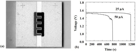
73] applied the LIFT technique to manufacture rechargeable Li-ion micro-batteries via Nd: YVO
4 laser (355 nm). The produced micro-battery and corresponding discharging behaviour are provided in
Figure 8.
Figure 8. (
a) Optical micrograph of Ag
2O/Zn alkaline micro-battery by LIFT, and (
b) discharging behavior of alkaline micro-batteries at 25 and 50 µg as a time function [
73]; with permission from Springer.
2.4. Applications of LIFT: Organics, Electronics, and Sensors
LIFT is a novel and unique technique alternative to incumbent techniques, e.g., inkjet printing, due to its capability to deposit pico-litre-sized droplets [
74]. This is beneficial for biological applications due to the use of a small quantity of reagent and a wide range of rheological properties. Besides, it can be executed in a simple lab environment. Using this method, specific and moderate depositions of complex molecules and eukaryotic cells show the exclusive capabilities of this technology. LIFT has a potential to print liposomes [
75], deoxyribonucleic acid [
18,
22,
76], and proteins [
77] with high resolution. Tissue printing is one of the latest applications of LIFT, proposed to replace burnt-cells [
78,
79]. These printed tissues behave like human osteosarcoma, endothelial and osteoprogenitor cells [
77,
80,
81] that have been successively printed. In-vivo and in-vitro testing was carried out on mice and showed excellent results [
82].
This technique is used to heat and light-sensitive materials, which cannot be irradiated by the pulsed-laser. For this purpose, organic light-emitting diodes (LEDs) [
83] and thin-film transistors (TFTs) [
78] have been printed by this method using different materials such as semiconductors and silver inks. Rapp et al. [
84] achieved an organic-TFT device using the LIFT technique. Distyryl-quaterthiophene (DS4T) was deposited on a donor substrate and transported with pico-second laser pulses on Si/SiO
2-based receiver substrate. The polymer layer showed high laser-absorption, and DS4T pixels printed on the receiver substrates presented excellent morphological properties. The LIFT technique manufactured polymeric LED via the decomposition of a thin triazene polymer film via a Xe-Cl excimer laser [
43]. The deposition process allows for the transfer of a bi-layer containing electroluminescent enclosed with an aluminum electrode. The soft transfer resulted in well-resolved pixels (=500 µm). Stewart et al. fabricated small molecules of Alq
3 organic-LED to produce RGB pixels [
85]. A coating of tetra-butyl ammonium hydroxide was placed at the aluminium cathode top to enhance the electron injection in the Alq
3, by more than 600%. The luminance and the efficiencies of these organic-LEDs were better than conventional LEDs in blue pixels.