2.1. Optical Modulators
Datacenter connections are the main driver for the R&D of Si photonics technology due to the ever-increasing data rate. They are moving from 25/100G to 100G/400G and optical transceiver modules have been developing toward 400G and beyond. In terms of that, Si optical modulators play an important role to satisfy the data rate. The development of modulators has been making it possible to take advantage of advanced modulation formats [
28,
29]. However, it is necessary to leverage heterogeneous integration for further improvement due to the limitation of Si’s poor electro-optic effect.
The properties of the light in Si waveguides are changed through a change of the optical constants of the waveguides, refractive index, and absorption coefficient. There are mainly two methods to change the effective refractive index, which are the thermo-optic effect and the plasma dispersion effect. The former is usually used in optical switches which don’t require the GHz regime high-speed operation and the latter is mostly used for high-speed Si modulators.
The plasma dispersion effect and free-carrier absorption are expressed by the Drude model, describing that changes in refractive index and absorption coefficient arise from a change in the plasma frequency of free carriers which is dependent on the number of free carriers and their conductivity effective masses. Thus, the changes in refractive index (Δ
n) and absorption coefficient (Δ
α) are expressed by
where
e is the electronic charge,
ε0 is the permittivity in a vacuum,
c is the speed of light in vacuum,
λ is the wavelength,
n is the unperturbed refractive index,
m*ce and
m*ch are the conductivity effective masses for electron and hole, and
μe and
μh is the mobilities for electron and hole, respectively [
16].
As shown in Equations (1) and (2), the parameters are physical constants except for the change in free-carrier densities. For Si, Soref and Bennett evaluated the changes in optical constants based on experimentally investigated results [
16] as shown in Equations (3) and (4) for 1.55-μm wavelength.
There are three different types of Si optical modulators as shown in . Electrical manipulation of free carriers interacting with the propagating light in the Si waveguide is achievable based on the types such as carrier accumulation, carrier injection, and carrier depletion. Carrier-accumulation and carrier-depletion types consist of semiconductor-insulator-semiconductor (SIS) and pn junction, respectively. They are more suitable for the high-speed modulation due to majority-carrier-based operation, compared to carrier-injection type comprised of pin junction. While the carrier accumulation type modulator requires an oxide barrier, the carrier-depletion type only requires a highly CMOS-compatible pn junction. Therefore, the latter is the most common approach due to relatively easy fabrication and simple design.
Figure 1. Cross-sections of typical device structures implementing the three different mechanisms (a) Carrier accumulation, (b) Carrier injection, and (c) Carrier depletion.
The
VπL of carrier-depletion type modulators with a horizontal
pn junciton is as high as 1.5 to 2.5 Vcm [
3,
29,
30,
31,
32,
33,
34]. Although the modulation efficiency can be reduced further by increasing free-carrier densities of the
pn junction, it results in high optical loss due to free-carrier absorption [
34]. In terms of that, the different shapes of vertical, L-shape, and U-shape
pn junctions can provide the larger modulation efficiency maintaining optical loss due to the larger mode overlap between the optical mode and larger junction area of the
pn junctions [
49,
50], but the larger junction area increases the junction capacitance, limiting modulation speed. The comparative analysis on optical modulators of both Si lateral and L-shape junctions has been reported. The tradeoff between static performance,
VπL, and phase-shifter loss, and dynamic performance,
fmod, is comparatively and quantitatively well investigated. In addition, such L-shape
pn junction-based modulators should be carefully designed considering
fmod, sacrificing
VπL to achieve target dynamic optical modulation amplitude (OMA) [
34].
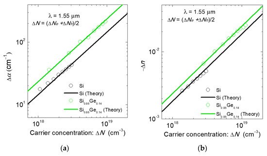
As can be seen in Si modulators above, it is important to introduce heterogeneous integration, taking advantage of materials with superior electro-optic effects in conjunction with an Si photonics platform. One of the materials is silicon germanium (SiGe). As shown in the plasma dispersion effect, Equation (1), the change in refractive index is inversely proportional to the effective masses of electrons and holes. Therefore, the lighter the conductivity masses become, the greater the plasma dispersion is. In CMOS technology, the application of strain to Si has been widely employed to achieve lighter conductivity masses and higher mobilities in the channels of transistors, which can improve MOS transistor’s performance. Tensile strain and compressive strain are introduced to Si for n-channel and p-channel MOS transistors, respectively. It was also experimentally reported that the plasma dispersion effect and free-carrier absorption in Si in the far-infrared wavelength range from 5 to 20 μm were modified by uniaxial strain mechanically applied to Si through strain-induced mass modulation [
51,
52]. On the other hand, strained SiGe is well-known as a p-channel material in CMOS technology due to its high hole mobility originated from the low effective mass of holes [
53,
54,
55,
56]. Therefore, it is expected to enhance the plasma dispersion effect. Y. Kim et al. experimentally showed strain-induced enhancement of plasma dispersion effect in silicon-germanium (SiGe) optical modulators. presents that the plasma dispersion effect and free-carrier absorption are enhanced by strain-induced mass modulation in strained SiGe.
Figure 2. Changes in optical constants of Si
0.86Ge
0.14 and Si as functions of carrier concentration. (
a) Change in refractive index and (
b) Change in absorption coefficient [
53].
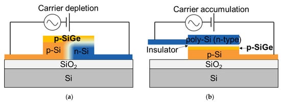
In 2018, Fujikata et al. demonstrated high-speed and highly efficient Si carrier-depletion type MZ modulators with a thin and strained SiGe layer [
57]. The device cross-sections are shown in a. The change in carrier profiles for carrier depletion in p-SiGe and n-Si regions is induced by applying reverse bias voltages e.g., under bias conditions of 0 and −2 V. p-SiGe is selectively grown on a Si waveguide and the crystal defects are barely shown in the Transmission Electron Micrograph (TEM) image in the reference. Based on the device performances of
VπL (0.67 Vcm, −0.5 V), 3-dB bandwidth (12 GHz at −1 V), and insertion loss (1.5 dB to 2.0 dB), the high-speed operation of 25 Gbps was achieved at near 1.3-μm wavelength. The
VπL is lower than typical lateral
pn junction Si modulators. Since the optical mode is near the center of the waveguide, it would be better to redesign the SiGe position so that mode overlap in SiGe can increase.
Figure 3. (
a) Schematic cross-sections of (
a) carrier depletion type [
57] and (
b) accumulation type [
58] modulators using a strained p-SiGe layer to enhance plasma dispersion effect.
Another method of heterogeneous integration is to apply the SIS structure for accumulation-based capacitive modulators. Additionally, it is more suitable for low driving voltage operation and power consumption thanks to the lower
VπL, compared to typical Si
pn junction-based modulators, which require traveling wave or multi-stage electrodes, and represent an extra-energy cost. M. Takenaka et al. proposed SiGe capacitive optical modulators as well as the theoretical background strain engineering of the enhanced plasma dispersion effect [
54]. In addition, it was demonstrated by M. Douix et al. in 2019, shown in b [
58]. Since strained SiGe technology is already used in CMOS technology, it was fabricated on a 300-mm Si photonics platform. As shown in b, SiGe is selectively grown on top of the bottom patterned Si-on-insulator (SOI) waveguide, followed by insulator deposition. Then, the top side waveguide is made up of poly-Si deposition. The position of the insulator was designed to be the center of the waveguide where the optical intensity is maximum, indicating optical mode overlap in SiGe is nearly maximized. The Si capacitive modulator without an SiGe layer was also prepared to compare with the device with SiGe. The phase shift against waveguide width and applied DC bias, with and without the strained SiGe layer was used for the comparison. SiGe device presents a 20% enhancement in efficiency due to higher hole efficiency in strained SiGe, resulting in
VπL as low as 0.27 Vcm with 4-nm oxide thickness. However, they showed dynamic characteristics of the SiGe device which
VπL is 1.08 Vcm with 13-nm taking into account an optimal tradeoff between device length, optical modulation amplitude, and electrical RC constant. The modulator response is limited to ~4 GHz, mainly limited by an access resistance. If optimized, device response is expected to be 10 times faster than the demonstrated device. In 2021, I. Charlet et al. have recently reported the optimized SiGe device can achieve 0.59 Vcm for
VπL and 37 GHz for 3-dB bandwidth, resulting in the dynamic OMA of −3 dBm at scattering propagation loss, 8 dB/cm [
59].
One main drawback of SiGe is that free-carrier absorption is also increased by strain-induced effective mass modulation with an increase in the plasma dispersion effect, which was also experimentally reported and shown in b. In terms of that, III-V materials have the advantageous inherent property in which free-carrier absorption is reduced while the plasma dispersion effect is enhanced for electrons [
60,
61,
62,
63,
64]. In 1990, B. R. Bennett et al. investigated the carrier-induced change in the refractive index of III-V compound semiconductors, InP, GaAs, and InGaAsP [
60]. Since the plasma dispersion effect is inversely proportional to the effective mass as shown in Equation (1), the light electron effective mass in III-V materials results in a greater change in the refractive index than that in Si. In addition, the bandfilling electro-optic effect and bandgap shrinkage contribute to the changes in the refractive index and absorption of n-type III-V materials. When the free carriers increase, the plasma dispersion effect and the bandfilling effect contribute to a negative refractive index change, while the bandgap shrinkage contributes to a positive change. Therefore, the plasma dispersion effect and the bandfilling effect are dominant for phase modulation. Importantly, they predicted the low-loss optical phase modulators and switches based on carrier modulation. In 2017, J. Han et al. demonstrated a highly efficient and low-loss InGaAsP/Si hybrid SIS-based capacitive modulator [
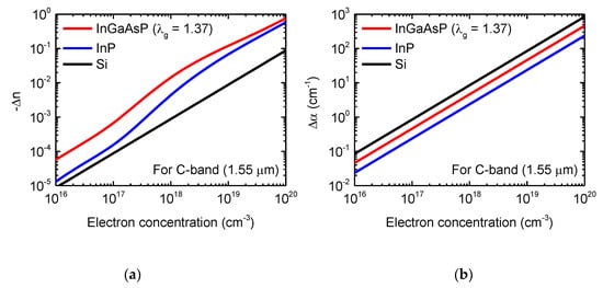
61]. They also reported the theoretical model, in which the change in refractive index is larger for InGaAsP and InP than Si, while the change in absorption coefficient is smaller than Si, as shown in a,b, respectively.
Figure 4. Numerical analysis of an InGaAsP/Si hybrid MOS optical modulator (
a) Electron-induced refractive index changes (Δ
n) of InGaAsP, InP and Si, (
b) Electron-induced absorption changes (Δα) of InGaAsP, InP and Si [
61].
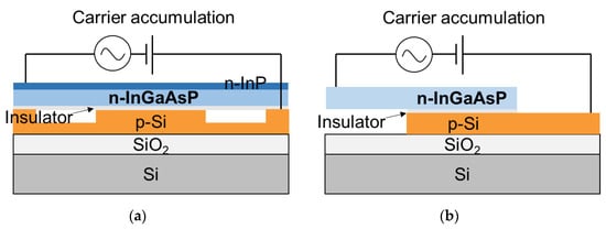
To heterogeneously integrate III-V on the Si rib waveguide, they used the wafer bonding technique. An InP substrate containing InGaAsP/InP layers was bonded on the Si waveguide using an Al2O3 bonding interface. a shows the device cross-section of the modulator, indicating optical mode is positioned near the SIS interfaces. They also investigated and optimized the interface quality to achieve a steep capacitance-voltage curve, which highly affects optical modulation. With 5-nm equivalent oxide thickness (EOT), they achieved a very low VπL of 0.047 Vcm due to InGaAsP and thin EOT. The phase shifter loss is around 20 dB/cm. Thanks to the low VπL, the device exhibited an extremely small attenuation of 0.23 dB for the 500-μm-long phase shifter. It is noticeable that the VπL and attenuation levels are one-order magnitude better than the conventional Si modulators. The experimental dynamic characteristics were not presented due to their high resistance and capacitance because the device was not optimized for high-speed operation. However, based on simulations, they mentioned that a high-speed modulation is also possible for the optimized III-V MOS modulator by showing eye diagrams of a 53-Gbaud 4-level pulse-amplitude modulation (PAM-4).
Figure 5. (
a) Cross-section of an InGaAsP/Si hybrid MOS optical phase shifter demonstrated by J. Han et al. [
61], and (
b) of InGaAsP/Si MOS capacitor phase-shifter demonstrated by T. Hiraki et al. [
62].
In the same year of 2017, T. Hiraki et al. also demonstrated heterogeneously integrated InGaAsP MOS capacitor MZ modulators [
62]. b shows the device cross-section the device was fabricated by the wafer bonding technique as well. Compared to J. Han et al.’s demonstration, it is more practically designed, taking into account the tradeoff between SiO
2 thickness and RC delay so that it can operate GHz-regime modulation. Therefore, the
VπL of 0.09 Vcm, is higher, but the cutoff frequency of ~2.2 GHz is faster than that in J. Han’s work. This dynamic performance enables a 32 Gbps modulation with signal pre-emphasis. They recently reported a high-efficiency MZ modulator integrated with a DFB laser using membrane InP-based devices on an Si photonics platform. The latest work [
63] shows a higher
VπL of 0.4 Vcm compared to their previous work, but the measured 3-dB bandwidth is around 31 GHz which is much more practical for high-speed modulators. Finally, they demonstrated eye diagrams with a 50-Gbps NRZ signal using the integrated DFB laser diode and high-efficiency InGaAsP MZM. From this work, it is important to design SIS-type modulator parameters, e.g., capacitance of an insulator, considering target data rate and bandwidth rather than demonstrating just extremely low
VπL. It is feasible for switch applications but not high-speed modulators.
The introduced heterogeneous III-V SIS modulators above are fabricated through wafer bonding with thin bonding layers and require metal contacts to the III-V material to realize the desired III-V-insulator-Si capacitive phase-shifter structures. Such process steps are quite challenging and less CMOS compatible, which may result in lower manufacturability and scalability. Integration of III-V on the Si platform through epitaxy has been investigated for the next-generation electronic and photonic devices in a CMOS pilot line [
65,
66]. Y. Kim et al. proposed the carrier-depletion monolithic III-V/Si optical phase modulator, leveraging the direct growth of III-V on Si V-groove [
67], and S. Kim reported its performance as predicted by TCAD simulations [
68]. The simulation study suggests the feasibility of a very low
VπL of 0.07 Vcm, a low phase-shifter loss of 16 dB/cm, and a very low α
VπL product close to 1VdB at 1.31 μm, which is 10 times lower than for typical Si
pn optical phase shifters. One of key issues is a defect-induced optical loss for a low loss phase shifter because it is difficult to achieve low enough defect density at the III-V/Si interface, where an optical mode exists.
Unlike the free-carrier effect, an applied electric field can change a material’s refractive index and so modulate the light using a linear electro-optic phenomenon known as the Pockels effect. The Pockels effect has none of the constraints of the free-carrier effect, which are unavoidable carrier induced loss due to free-carrier absorption and limited operating speed due to carrier lifetime for carrier injection type or RC delay for carrier depletion type. However, Si has almost no Pockels effect since it does not exist in a centrosymmetric crystal, indicating that it is difficult for Si to take advantage of the Pockels effect. Therefore, the leveraging of such materials with a non-centrosymmetric crystal structure and strong Pockels effect on a Si photonics platform for high-performance optical phase shifters has been investigated. Lithium niobate, LiNbO
3 (LN), with a Pockels coefficient around ~30 pm/V, is one of the most popular materials for electro-optical modulators with the role of external modulation in fiber-optic transmission systems. The LN modulators are typically fabricated using LN substrates and titanium diffusion and proton exchange are used for LN waveguide formation with a refractive index contrast of ~0.04, which is much smaller than that in Si photonics. Therefore, the off-the-shelf LN modulators are bulky and power-consuming with a large
VπL of more than 10 Vcm. There have been many efforts to make bulky LN modulators integrated so that they can support capacity-hungry short reach links such as data-center interconnects. For high refractive index contrast and flexibility in fabricating nanostructures, a thin-film lithium niobate platform was proposed [
69], and high-performance coherent optical modulators were demonstrated on the LN-on-insulator platform [
70,
71,
72]. Furthermore, the hybrid approach of Si and LN MZ modulators was demonstrated by M. He et al. in 2019 [
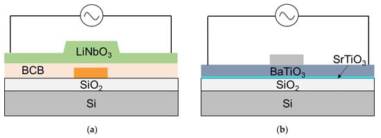
73]. a shows the schematic of the hybrid Si/LN modulator, which was fabricated by the die-to-wafer using benzocyclobuten (BCB) adhesive and LN dry etching technique. The modulator is composed of passive components of Si grating couplers, Si MMI couplers, and Si waveguides, and active components of LN-based phase-shifters. One of the important parts, which enable it to be hybrid, are the vertical adiabatic couplers (VACs), which transfer the optical power between Si and LN membrane waveguides (>97%, loss of ~0.19 dB per VAC). The hybrid Si/LN modulator with the LN phase shifter length of 5 mm exhibits an insertion loss of 2.5 dB,
VπL of 2.2 Vcm, electro-optic bandwidth of at least 70 GHz, and modulation rates up to 112 Gbps.
Figure 6. (
a) Schematic cross-sections of (
a) LN/Si optical phase shifter [
73] and (
b) BTO/Si optical phase shifter using Pockels effect [
75].
Simply, if the stronger Pockels effect can be used, a smaller device footprint is available. Regarding the strong Pockels’ material, barium titanate, BaTiO
3 (BTO) crystals have a Pockels coefficient of 1600 pm/V, more than 50 times higher than LN. In addition, they can also be epitaxially grown as thin films on an Si substrate. Therefore, BTO emerges as a highly promising material to achieve Pockels electro-optic modulators integrated on a Si photonics platform [
74,
75,
76,
77]. First, S. Abel et al. demonstrated a large Pockels effect in micro- and nanostructured BTO integrated on Si [
74], as shown in b. They fabricated photonic and plasmonic devices employing BTO growth on SOI wafers by molecular beam epitaxy and wafer bonding and verified the Pockels effect to be the physical origin of the response, with the Pockels coefficient tensor element,
r42 = 923 pm/V. F. Eltes et al. reported a monolithically integrated BTO-based optical modulator on a Si photonics platform targeting a next-generation platform [
75]. The same method reported in [
74] was used to integrate BTO into EPIC. The only difference is the host wafer which is an electronic and photonic integrated circuits (EPIC) processed substrate, instead of a bare SiO
2/Si wafer. The integrated BTO/Si MZ modulator shows excellent
VπL of 0.2 Vcm and α
VπL of 1.3 VdB (~0.7 VdB when optimized), indicating ~5.7 dB/cm (~3.0 dB/cm when optimized) and works at high speed of 25 Gbps, which is expected to reach data rates >50 Gbps by an adapted electrode design. Here, one feature of the optical modulators based on the Pockels effect are that they can be operated at cryogenic temperatures, whereas free-carrier effects-based optical modulators are restricted at low temperatures [
76]. This is expected to encourage the use of Si photonics for quantum computing in the future.
2.2. Optical Switches
Optical switches are also important components for large-scale data center interconnections [
45]. Although free-space optical switches realized by micro-electromechanical systems (MEMS) [
44,
46] and liquid crystal on silicon (LCOS) [
47] have been already commercialized for large-scale data center application, these approaches have disadvantages, such as high cost owing to its high process complexity and the difficulty of high-volume manufacturing [
45,
48,
78,
79,
80]. To overcome these problems, lithography-based fabrication, especially CMOS-compatible integrated photonics, has been widely investigated [
45,
48,
78,
79,
80].
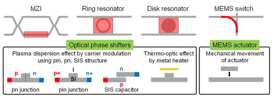
To achieve integrated optical switches, several approaches have been suggested. Although electro-optic effects are the main modulation principles for the optical modulators [
42], other principles, such as a thermo-optic effect [
43] or MEMS actuators [
44], are also widely used for optical switches to achieve high scalability and low crosstalk. In the case of the electro-optic optical and thermo-optic switches, an optical phase shifter is implanted into the interferometer or resonator structures as shown in ; thus, efficient modulation schemes discussed in previous captures are also partially effective for high-performance optical switches. On the other hand, the MEMS actuators of MEMS optical switches made by poly-Si or silicon-on-insulator (SOI) are mechanically moved to connect each optical pass. In this section, the recent progress on the integrated optical switches is discussed.
Figure 7. Schematics of various optical switches in large-scale Si PICs.
The thermo-optic switches [
81,
82,
83,
84] and MEMS optical switches [
85,
86,
87,
88] are commonly investigated to achieve large scalability and low crosstalk. These structures have relatively small losses compared to the electro-optic effect due to no carrier response; thus, they can achieve small crosstalk. Particularly in the case of MEMS optical switches, it is easier to design a large-scale switch array with small complexity and crosstalk because they need no multi-stage interferometers or resonators [
89]. However, the optical loss caused by structure parameters, such as the distance between a metal heater and the waveguide [
90] and the distance between a MEMS actuator and the waveguide [
91,
92], is the main drawback of these structures. Relatively low speed and large power consumption are also the main issues on these devices. MEMS optical switches can also achieve small power consumption; however, a large driving voltage up to 60 V is necessary to move the MEMS actuator, which makes CMOS compatible integration difficult.
Si-based carrier modulation structures such as
pin or p-n junction are commonly researched thanks to their high CMOS compatibility, although their electro-optic effect is relatively small compared to other materials [
42]. Although the optical switches using the carrier injection with a
pin junction [
93,
94] is the main principle to achieve large phase modulation, its speed and power consumption suffer owing to the minority carrier response in Si compared to the modulators mainly using a
pn junction [
42]. The feasibility of the optical switches using a p-n junction is reported to achieve high-speed operation and low power consumption [
95]. However, due to large carrier-induced loss for phase modulation, the crosstalk of Si
pn and
pin structures is worse compared to other structures [
45,
46,
47,
48].
To achieve the large phase shift using the semiconductor, III-V compound semiconductors, especially InP-based materials, have been investigated. Bulky III-V devices using a semiconductor optical amplifier (SOA) [
96,
97,
98] or
pin junction are demonstrated [
99]. These structures can achieve relatively small crosstalk compared to Si devices thanks to the large electro-optic effect of III-V materials. However, Bulky III-V photonics has its problems, such as poor optical confinement, deep trench, and scalability [
100]. To overcome these problems, a III-V on insulator structure is suggested [
100]. The
pin optical switch using this III-V on the insulator platform is reported [
101]. The hybrid integration of Si and III-V is also investigated to overcome the disadvantages of III-V devices by many groups [
102]. Many structures have been demonstrated such as a III-V/Si hybrid SOAs [
103,
104], and a III-V/Si hybrid semiconductor-insulator-semiconductor (SIS) capacitor [
105]. The III-V/Si hybrid SIS structure can achieve relatively small crosstalk and small power consumption owing to its large electron phase modulation efficiency and the small leakage current of an SIS structure [
105].
Recently, programmable optical switches have been actively investigated for a neuromorphic photonics application [
106]. There are many reports on optical phase shifter arrays for this application, controlled by external signal [
106]. For further development, to achieve efficient and multi-functional photonics switches for these applications, the non-volatile or bi-stable operation of the optical switches has been widely investigated using a phase-change material (PCM) [
107], a ferroelectric BaTiO
3 (BTO) [
108], or an MEMS switch [
109]. However, the high optical loss due to the metal phase of PCM and the process complexity of non-CMOS-compatible materials are the main problems with these approaches. Recently, CMOS-compatible ferroelectric materials, such as HfZrO
2, are widely investigated for electrical devices. These CMOS compatible ferroelectric materials can also achieve efficient phase shift thanks to their large carrier accumulation enhancement using the negative capacitance effect [
110]. The feasibilities of non-volatile operation for the optical switch application are also reported [
111].

