Perovskite solar cells (PSCs) with earth-abundant carbon as an effective replacer for unstable hole transporting materials and expensive electrodes is a recently proposed structure promising better air and moisture stability. Herein,the latest advances and state of the art of Pb-free and low Pb content perovskites, used as absorbers in carbon based perovskite solar cells are described in this entry. The focus is on the implementation of these, environmentally friendly and non-toxic, structures in PSCs with a carbon electrode as a replacement of the noble metal electrode typically used (C-PSCs). The motivation has been the great potential that C-PSCs have shown for the leap towards the commercialization of PSCs. Some of their outstanding properties include low cost, high stability, ambient processability and compatibility with most up scaling methods (e.g. printing).By surpassing the key obstacle of toxicity, caused by the Pb content of the highest performing perovskites, and by combining the advantages of C-PSCs with the Pb-free perovskites low toxicity, this technology will move one step further.
1. Introduction
Perovskites, which are materials with the crystal structure similar to calcium titanium oxide (CaTiO
3), were first discovered in 1839, when the Russian mineralogist L. A. Perovski discovered the mineral CaTiO
3. However, it was not until the late 1990s, when the structural dynamics of methylammonium lead iodide perovskite (MAPbI
3) material were studied and explored for application in optoelectronics, such as thin-film transistors, photovoltaics (PV) and light-emitting diodes [
1,
2]. Since then, huge leaps of progress have been made and perovskites have been implemented in high-performing solar cells [
3], light-emitting diodes [
4], photodetectors [
5], lasers [
6], as well as sensors, fuel cells, superconductors, catalysis and more [
7,
8].
The greatest progress and the most intensive research have been towards the application of perovskites as absorbers for solar energy conversion applications. In that direction, perovskite solar cells (PSCs) have achieved power conversion efficiencies (PCEs) that are now comparable with the traditional, well-established and widely applied technology of Si solar cells. Among the different perovskite structures, the perovskite of the organic-inorganic metal halide (OIH) group are the ones that systematically achieve the highest PCEs that are being reported. However, even though PSCs count more than 10 years of extensive study and optimizations, there is still a gap towards the commercialization of this technology. This barrier is mainly caused by three factors: (i) the reduction of PCE when moving to large area devices, (ii) the questionable stability of PSCs under real-life working conditions and (iii) the toxicity of the starting materials, most of all the lead (Pb) content.
For the up scaling of PSCs, a lot of effort has been invested in the device engineering and construction methods, which has led to large area devices with PCEs exceeding 15% [
9,
10]. The sources of perovskite instability include, among others, water and moisture degradation, thermal stress, light and oxygen induced degradation, ion migration and corrosion of the back contact [
11]. One of the most efficient and promising methods to overcome these problems, originating from the corrosion of the metal electrode, is turning it into a different type of PSC: Carbon electrode-based Perovskite Solar Cells (C-PSCs).
In a typical structure, PSCs comprise of a multilayered device architecture of the absorber “sandwiched” between an electron transport layer (ETL) and a hole transport layer (HTL), while the circuit is completed by a metal back electrode, most commonly Au or Ag. During the long-term operation of PSCs, the migration of iodine and metals, combined with the formation of metal halide ions and oxygen vacancies, start to corrode the metal electrode, leaving the structure exposed to the environment and causing a slow degradation [
12,
13]. In C-PSCs, the metal electrode is replaced by a carbon (C) electrode. Carbon has an appropriate work function (W
F) of −5 eV to qualify for an efficient charge collector, while at the same time its hydrophobic nature repels oxygen and moisture from the ambient, providing a protective barrier for the perovskite layer. At the same time the inertness of C allows to remain unaffected by ion migration. This has enabled devices with long-term stability to be achieved, without the need for encapsulation [
14].
Being on a track with significant advances in the aspect of overcoming the two out of three barriers which hinder the commercialization of PSCs, the remaining obstacle that needs to be tackled is the environmental and health issues caused by the toxicity of Pb and other perovskite precursor components, such as the HTL and perovskite additives. The European Union has imposed strict rules on the use of toxic elements in consumer electronics. If this problem is not resolved, the PSC technology is bound to remain in lab scale and research level. Hence, the last years have seen lots of efforts for the partial or total elimination of Pb, and its substitution by other metals, which are less toxic and environmentally and health friendly. Most of the research has been focused on the typical metal electrode structure PSCs, since it is the one that exhibits the highest PCEs so far; however, with the continuous rise of C-PSCs and their additional advantage of stability and significantly lower cost than the metal electrode PSCs, it is prominent that there needs to be a turn to low-toxicity materials’ implementation in C-PSCs as well.
2. Carbon-Based Perovskite Solar Cells (C-PSCs)
2.1. General Description
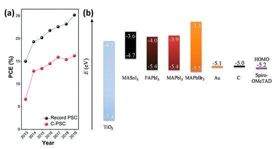
Carbon-based perovskite solar cells (C-PSCs) differ from the traditional structures in that the metal electrode is eliminated, replaced by a carbon electrode typically prepared using simple methods, such as doctor blading, screen printing and painting, by a C paste. Depending on the temperature that is required for the annealing of the C paste, in order for the electrode to form, they can be distinguished in two main categories: high-temperature (HT) and low-temperature (LT) C-PSCs. Both structures have the same working principle: upon illumination, excitons are produced by the perovskite absorbing layer, forming free charge carriers (electrons and holes); electrons are drawn to the electron transport layer (ETL) and holes are collected from the hole transport layer (HTL). The C electrode, having an appropriate work function (WF), similar to Au, and Fermi level above the valence band edge of the perovskite, can draw the carriers to the external circuit. Moreover, carbon has the capability to absorb oxygen and moisture, thus protecting the perovskite and providing highly stable devices. Even though the initial reports of C-PSCs achieved PCEs much lower than the conventional devices, typically below 10%, the intensive research in this field has led to optimized devices with comparable PCEs to the high-performing metal electrode PSCs, with higher stability and at a significantly lower cost ().
Figure 1. (
a) Summary of development in PCEs of C-PSCs in comparison to state-of-the-art PSCs [
15]. Reproduced with permission—Copyright 2020 Royal Society of Chemistry. (
b) schematic energy level diagram of perovskite materials, TiO
2, Spiro-OMeTAD, Au and C [
16]. Reproduced with permission—Copyright 2017 Wiley-VCH.
2.2. High-Temperature (HT) C-PSCs
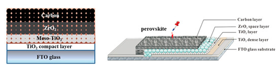
The representative HT device configuration comprises of multiple oxide layers on top of which the perovskite is deposited and formed after annealing. In particular, a compact hole blocking layer, typically TiO2 or SnO2 grown from precursor solutions, is first deposited on FTO glass substrates, to minimize recombination losses and prevent shunting pathways. Next, an Electron Transport Layer (ETL) is deposited, which is most commonly the wide bandgap semiconductor Titanium Dioxide (TiO2) in a mesoporous structure, followed by an additional mesoporous layer, typically ZrO2 or AlO3. This layer acts as a spacer, preventing the direct contact of TiO2 with the C electrode, which would cause a short circuiting of the device. Finally, the mesoporous C electrode is deposited from a starting C paste, which is then annealed at a high temperature to remove binders and organic substances and increase the conductivity of the resulting electrode. The perovskite precursor solution is then infiltrated through the triple mesoscopic stack and the perovskite film is formed after annealing (). This type of devices are also referred to as “monolithic” and additionally to being HTL-free, highly stable and able to be prepared under ambient conditions, they can also be entirely prepared by printing methods, which gives an advantage when moving to up scaling.
Figure 2. A schematic structure of a HT carbon-based “monolithic” perovskite solar cell [
17] and the corresponding device illustration [
18]. Reproduced with permission—Copyright 2013 Nature Publishing Group.
A variety of carbon materials have been used in order to prepare high-performing C pastes, which would result in C electrodes of high conductivity, low series resistance and great mechanical stability. Among these, the combination of carbon black (CB) and graphite has been established as a high-performing formulation [
18,
19,
20,
21], while carbon nanotubes (CNTs) have also shown promising results [
22,
23]. In all of the highest-performing HT C-PSCs the perovskite formulations that have been used are Pb-based, with the most common being the AVA
xMA
(1−x)PbI
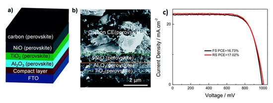
3, while recently efforts have turned to the incorporation of multiple cation structures, for the enhancement of performance and stability (). In the typical HT C-PSC structure, no HTL is employed; however, the state of the art PSCs of this structure have achieved PCE of 17%, when a Nickel Oxide (NiO) layer has been employed as the HTL [
24], combined with a mixed cation-mixed halide perovskite ().
Figure 3. (
a) Schematic architecture of the C-PSC consisting of FTO glass as a transparent substrate, a compact TiO
2 layer, a mesoporous TiO
2 layer, an Al
2O
3 layer and NiO layer coated with graphite/carbon black CE; (
b) cross section SEM image of device with TiO
2/Al
2O
3/NiO/C (Cs
x(FA
0.4MA
0.6)
1−xPbI
2.8Br
0.2) structure; (
c) J-V curves of champion perovskite solar cell devices under standard AM 1.5G illumination at 100 mWcm
−2 [
24]. Reproduced with permission—Copyright 2017 Royal Society of Chemistry.
Table 1. Summary table of some of the highest-performing HT C-PSCs that have been reported so far.
| PCE (%) |
Perovskite |
HTL |
Device Configuration |
Carbon Paste Formulation |
Year/Reference |
Comments |
| 17.02 |
Cs0.05(FA0.4MA0.6)0.95PbI2.8Br0.2 |
NiO |
FTO/c-TiO2/mp-TiO2/Al2O3/NiO/C |
Graphite/carbon black |
2017 [24] |
sequential deposition |
| 16.51 |
(5-AVA)x(MA)1−xPbI3 |
- |
FTO/c-TiO2/mp-TiO2/ZrO2/C |
Commercial C paste |
2020 [25] |
PBS-X; X = Li, Na, and K post treatment of TiO2/ZrO2/C |
| 16.37 |
MAPbI3 |
- |
FTO/c-TiO2/mp-TiO2/PbTiO3/CNTs |
CNTs sprayed |
2019 [23] |
ultrathin layer of ferroelectric PbTiO3 on the TiO2 scaffold |
| 16.26 |
Cs0.1Rb0.05FA0.85PbI3 |
- |
FTO/c-TiO2/mp-TiO2/ZrO2/ C |
Carbon/spheroidal graphite |
2019 [26] |
1. DMF:DMSO: Formamide mixed solvent
2. Evaporation control |
| 15.9 |
CH3NH3PbI3(SrCl2)x |
- |
FTO/c-TiO2/mp-TiO2/Al2O3/C |
Graphite/ carbon black |
2016 [27] |
SrCl2 chemical modification of perovskite |
| 15.77 |
(5-AVA)x(MA)1−xPbI3 |
- |
FTO/c-TiO2/mp-TiO2/ZrO2/C |
carbon black/graphite |
2019 [28] |
VOx post-treatment of C/perovskite interface |
| 15.7 |
(5-AVA)x(MA)(1−x)PbI3 |
- |
FTO/c-TiO2/mp-TiO2/ZrO2/C |
Graphite/ carbon black |
2018 [29] |
oxygen-rich carbon black |
| 15.6 |
CH3NH3PbI3 |
- |
FTO/c-TiO2/mp-TiO2/ZrO2/C |
Carbon/spheroidal graphite |
2017 [30] |
1.additive of ammonium chloride (NH4Cl)
2. Two-step process during perovskite formation |
| 15.6 |
AB-MAPbI3 |
- |
FTO/c-TiO2/mp-TiO2/ZrO2/C |
Graphite/ carbon black |
2017 [31] |
1. 4-(aminomethyl) benzoic acid hydroiodide (AB) organic cation
2. benzylamine hydroiodide (BA)benzylamine hydroiodide (BA) organic cation
3. 5-AVAI organic cation |
| 15.11 |
(5-AVA)x(MA)1−xPbI3 |
- |
FTO/c-TiO2/mp-TiO2/ZrO2/C |
Graphite/ carbon black |
2019 [32] |
1. Ethanol co-solvent in GBL |
| 15.03 |
CH3NH3PbI3 |
NiO |
FTO/c-TiO2/mp-TiO2/Al2O3/NiO/C |
Graphite/ carbon black |
2015 [33] |
quadruple-layer architecture |
| 15 |
CH3NH3PbI3 |
- |
FTO/c-TiO2/mp-TiO2/Al2O3/C |
Graphite/ carbon black |
2017 [34] |
1. NMP solvent
2. slow crystallization (SC) method |
| 15 |
Cs0.1FA0.9PbI3 |
- |
FTO/c-TiO2/mp-TiO2/ZrO2/C |
Commercial C paste |
2019 [35] |
Prepared in glove box |
| 14.9 |
CH3NH3PbI3 |
NiO |
FTO/c-TiO2/mp-TiO2/ZrO2/NiO/C |
Graphite/ carbon black |
2015 [36] |
sequential deposition |
| 14.7 |
CH3NH3PbI3 |
- |
FTO/c-TiO2/mp-TiO2/Al2O3/C |
SWCNTs/carbon black |
2016 [22] |
SWCNT-doped graphite/carbon black electrode |
| 14.5 |
MAPbI3−xClx |
- |
FTO/c-TiO2/mp-TiO2/ZrO2/C |
Carbon/spheroidal graphite |
2018 [37] |
Addition of 0.45M MACl increases PCE from 8.74% to 14.5% |
| 14.5 |
CH3NH3PbI3 |
- |
FTO/c-TiO2/mp-TiO2/ZrO2/C |
N/A |
2016 [38] |
Effect of LiCl additive |
| 14.3 |
(5-AVA)x(MA) (1−x)PbI3 |
- |
FTO/c-TiO2/mp-TiO2/ZrO2/C |
Commercial C paste |
2017 [39] |
humidity assisted thermal exposure (HTE) as a post-treatment method—150 h |
| 14.27 |
CH3NH3PbI3-xGuCl |
- |
FTO/c-TiO2/mp-TiO2/ZrO2/C |
Commercial C paste |
2016 [40] |
1. Additive GuCl in perovskite
2. Voc 1.02V |
| 14.2 |
CH3NH3I |
NiO |
FTO/c-TiO2/mp-TiO2/ZrO2/NiO/C |
carbon black/graphite |
2015 [41] |
1. NiO nanosheet paste on ZrO2
2. Comparison of nanoparticles and nanosheets.
3. Screen printed device |
2.3. Low-Temperature (LT) C-PSCs
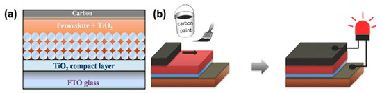
The low-temperature C-PSC configuration, besides the obvious difference of the C paste requiring a low-temperature annealing to form the C electrode, differs from the HT in two major aspects: (a) the C electrode is deposited after the perovskite deposition and crystallization on the appropriate substrate and (b) the mesoporous layers can be omitted and replaced by planar ones. Particularly for the spacer layer, this can be entirely eliminated, since the perovskite layer intervenes between the C electrode and the ETL, thus preventing a short circuit at this interface. This type of devices are also referred to as “paintable” ().
Figure 4. (
a) Schematic illustrating the cell architecture [
42]. Reprinted with permission from Zhang, F.; Yang, X.; Wang, H.; Cheng, M.; Zhao, J.; Sun, L.
ACS Appl. Mater. Interfaces 2014,
6, 16140–16146-Copyright 2014 American Chemical Society and (
b) fabrication process of LT “paintable” perovskite solar cells [
43]. Reproduced with permission—Copyright 2016 Wiley-VCH.
The carbon pastes that are being used typically consist of carbon black, graphite, polymer, additive and a non-polar solvent. In this type of C-PSC, it is crucial that the components of the paste are compatible with the underlying perovskite layer, in order to avoid its decomposition. It is noteworthy that this architecture benefits the use of free-standing electrodes as well as electrodes that are simply press transferred on the perovskite layer, giving the opportunity for high efficiency devices with an ease of fabrication and an extremely low cost [
44,
45,
46,
47]. Additionally, in this structure the perovskite is grown directly on the ETL, avoiding the infiltration through multiple mesoporous layers. This gives a much higher flexibility and a variety of choices for the perovskite structures to be used. This has led to devices with PCEs comparable to the ones of Au-based devices, owing to the potential of multiple cation, multiple halide perovskites for high-performance and high-stability devices, as summarized in . The current state-of-the-art LT C-PSC has achieved PCE of 19.2%, in devices with self-standing C films used as counter electrode, mixed cation perovskite structure and spiro-OMeTAD as the HTM [
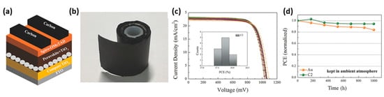
44] ().
Figure 5. (
a) Schematic diagram of C-PSCs; (
b) the roll-up of C films; (
c) Uniform performance of devices based on C films rolled up for a week; (
d) stability test of C-PSCs kept in ambient atmosphere without any encapsulation [
44]. Reproduced with permission—Copyright 2018 Wiley-VCH.
Table 2. Summary table of some of the highest-performing LT C-PSCs that have been reported so far.
| PCE (%) |
Perovskite |
HTL |
Device Configuration |
Carbon Paste Formulation |
Year/Reference |
Comments |
| 19.2 |
(FA0.75MA0.25)PbI2.75Br0.25 |
spiro-OMeTAD |
FTO/c-TiO2/mp-TiO2/perovskite/spiro-OMeTAD/C |
Commercial C paste |
2018 [44] |
self-standing films |
| 18.65 |
Cs0.05(MA0.17FA0.83)0.95Pb(I0.83Br0.17)3 |
spiro-OMeTAD |
FTO/c-TiO2/mp-TiO2/perovskite/spiro-OMeTAD/C |
Graphene in IPA |
2019 [48] |
various commercial carbon sources (carbon black, graphite sheet, and graphene) studied |
| 18.22 |
FA0.3MA0.7PbI3 |
P3HT/graphene |
FTO/SnO2@TiO2/perovskite/P3HT/C |
C in propylene glycol monomethyl ether acetate |
2019 [49] |
Stability 89% of original PCE after 600 h |
| 18.1 |
(FA0.83MA0.17)PbI2.15Br0.85 |
CuSCN |
FTO/c-TiO2/mp-TiO2/perovskite/CuSCN/C |
graphitic carbon layer |
2019 [50] |
≈95% of their initial efficiencies for >2000 h under full-sun illumination |
| 17.78 |
Cs0.05(MA0.17FA0.83)0.95Pb(I0.83Br0.17)3 |
CuPc |
FTO/Zn:SnO2/perovskite/CuPc/C |
Commercial C paste |
2019 [51] |
Zn-doped SnO2 ETL |
| 17.58 |
Cs0.05(FA0.83MA0.17)0.95Pb(I0.83Br0.17)3 |
CuSCN |
FTO/c-TiO2/mp-TiO2/perovskite/CuSCN/C |
MWCNTs in chlorobenzene |
2019 [52] |
1. MWCNTs to replace carbon black
2. Stability 80% after 1000 h 1 sun illumination |
| 17.56 |
FACsPbI3 |
spiro-OMeTAD |
ITO/SnO2/perovskite/spiro-OMeTAD/C |
free-standing CNT sheet |
2018 [46] |
Trifluoromethanesulfonic acid vapor doping of the free-standing CNT sheet enabled tuning of conductivity and work function of electrode |
| 17.46 |
Cs0.05(FA0.4 MA0.6)0.95PbI2.8Br0.2 |
CuPc |
FTO/Ni:TiO2/perovskite/CuPc/C |
Commercial C paste |
2018 [53] |
1. planar
2. Ni-doped rutile TiO2 as electron transport layer |
| 17.02 |
Cs0.05(FA0.85MA0.15)0.95Pb (I0.85Br0.15)3 |
spiro-OMeTAD |
FTO/SnO2/perovskite/spiro-OMeTAD/C |
Self-adhesive carbon film |
2020 [45] |
1. planar
2.graphite paper/carbon film electrode |
| 16.6 |
Cs0.05 (MA0.17FA0.83)0.95Pb(I0.83Br0.17)3 |
spiro-OMeTAD |
FTO/c-TiO2/m-TiO2/perovskite/C |
SWCNT film |
2017 [54] |
1. press-transferred single-walled carbon nanotube (SWCNT) film infiltrated with Spiro-OMeTAD
2. superior long-term stability at elevated temperatures |
| 16.25 |
FAxMA1−xPbIy Br3-y |
- |
ITO/SnO2/MWCNTs:perovskite/C |
Commercial C paste |
2019 [55] |
1. MWCNTs additive in the perovskite solution
2. all air processed
3. stability 93% under ambient air conditions for 22 weeks |
| 16.2 |
MAPbI3:MAPbIxBr3−x |
- |
FTO/c-TiO2/m-TiO2/perovskite/C |
Commercial C paste |
2019 [56] |
MAPbI3/MAPbIxBr3−x perovskite stacking structure |
| 16.1 |
MAPbI3 |
CuPc |
FTO/c-TiO2/m-TiO2/perovskite/CuPc/Carbon |
Commercial C paste |
2016 [57] |
8.5% drop during 600 h durability tests |
| 16.03 |
MAPbI3 |
- |
ITO/HMB:C60/perovskite /C |
Commercial C paste |
2019 [58] |
1. hexamethonium bromide-doped fullerene C60 ETL
2. No hysteresis |
| 15.73 |
CH3NH3PbI3–SWCNT |
- |
FTO/c-TiO2/m-TiO2/perovskite/SWCNT–C |
flaky graphite/spheroidal graphite/ carbon black |
2019 [59] |
1. SWCNTs in both anti-solvent and C electrode
2. stability of 90 days in dark under high humidity and high-temperature conditions |
| 15.6 |
Cs0.05MA0.16FA0.79Pb(I0.84Br0.16)3 |
- |
FTO/c-TiO2/m-TiO2/perovskite/PEA2PbI4/C |
Commercial C paste |
2018 [60] |
1. 2D perovskite interlayer
2. Stability 92% of initial PCE after 1000 h of exposure to ambient conditions |
| 15.38 |
MAPbI3 |
- |
FTO/C60/perovskite/C |
Commercial C paste |
2018 [61] |
1. First report on fullerene ETL
2. Additional replacement of FTO with graphene based TC electrode |
| 15.29 |
Cs0.04(MA0.17FA0.83)0.96Pb(I0.83Br0.17)3 |
spiro-OMeTAD |
FTO/c-TiO2/m-TiO2/perovskite/C+spiro-OMeTAD |
Commercial C paste |
2016 [62] |
Carbon cloth embedded in C paste electrode |
| 15.27 |
MAPbI3:MA1−xCsxPbI3 |
- |
FTO/c-TiO2/m-TiO2/perovskite/C |
Graphite/carbon black |
2020 [63] |
Post treatment with acetate salts (CsAc, FAAc, MAAc, KAc, NaAc) |
| 15.23 |
MAPbI3 |
- |
FTO/c-TiO2/m-TiO2/m-Al2O3/perovskite/C |
MWCNTs in chlorobenzene |
2017 [64] |
Boron doping of MWCNTs for enhanced hole extraction |
As the interest in C-PSCs is rising, so are the PCE values that are achieved and C-PSCs have now been established as the most promising structure for large-area applications and potential commercialization of perovskite solar modules, owing to their high stability, capability to be processed entirely under ambient conditions, the ability to be HTL-free and, most importantly, their significantly lower cost compared to PSCs with metal electrodes. Hence, it is expected that more progress will be presented in the near years to come. One of the most challenging tasks will be to implement environmentally friendly perovskite structures in C-PSCs, in order to overcome the additional barrier of PSCs towards their commercialization, which are the toxicity issues caused by the Pb content of the perovskite.
3. Perovskites
3.1. General Description-Current State of the Art
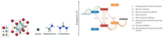
Hybrid organic-inorganic lead halide perovskites are compounds with the general chemical formula ABX3 and octahedral structure. A is the component that generally forms the unit cell and is an organic monocation, typically CH3NH3+ (methylammonium-MA), HC(NH2)2+ (formamidinium-FA) or the inorganic cesium (Cs+). Component B is a, smaller than A, divalent metal cation, most commonly Pb2+ or Sn2+, which is located in the center of the cube unit cell, and X is an anion, typically a halogen such as Cl−, Br− or I− ().
Figure 6. The ABX
3 perovskite crystal structure and the atomic structure of three A site cations explored. B is Pb or Sn, and X is a halogen ion [
65]. Reproduced with permission—Copyright 2014 Royal Society of Chemistry. On the right side the energy level diagram, showing the processes occurring during a PSC of the normal structure operation is depicted.
Organic-inorganic hybrid perovskites possess optoelectronic properties that make them suitable for applications as photoactive materials in solar cells. These features include high absorptivity, high charge carrier mobility, long exciton diffusion length, tunable bandgap and low exciton binding energy. The CH
3NH
3PbI
3 and CH
3NH
3PbBr
3 perovskites were first studied and presented as sensitizers in Dye Sensitized Solar Cells (DSSCs) which demonstrated moderate PCE of 3.81% [
66]. After that, device engineering, materials composition and chemical modifications have enabled PCEs to rise rapidly and reach 25.5% in 2021 [
67], 12 years after their first appearance in the solar cell community. The highest-performing devices, exhibiting PCEs that exceed 20%, employ MA and/or FA as the A cation and Pb as the B cation. Even though the performance of the perovskite based SCs is now comparable in terms of efficiency and stability with Si SCs, at the same time with a much lower cost, there is a major issue towards the commercialization and real-life application of this technology that needs to be tackled, and this is the toxicity and environmental harmfulness of Pb. Especially in consumer electrical and electronic equipment, the use of hazardous materials is prohibited and considering that Pb has been identified as one of the ten hazardous chemicals listed by ROHS in order to avoid its exposure to environment and people, it is mandatory that its use is limited [
68,
69] (). Thus, Pb-based perovskites are unlikely to see a broad industrialization in order to compete with other photovoltaic technologies, unless there is turn to lead-free perovskite materials that would provide stable devices with acceptable PCEs, without endangering the human health and the environment [
70].
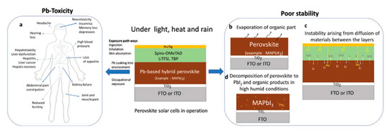
Figure 7. Schematic illustration of (
a) effect of exposure of toxic-lead on human life and (
b–
d) factors responsible for the perovskite degradation [
71]. Reproduced with permission—Copyright 2019 Wiley-VCH.
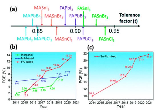
Towards that direction, the most promising candidates that have been investigated as substitutes of Pb are Tin (Sn), Germanium (Ge), Bismuth (Bi), Antimony (Sb) and Copper (Cu).
Tin is considered to be the most suitable candidate for Pb substitution, because of its similar valence electronic configuration and ionic radius (Sn
2+ = 115 pm and Pb
2+ = 119 pm) [
72]. Sn-based perovskites have the general formula of ASnX
3, A being MA
+, Fa
+ or Cs
+ cation, and X a halogen anion. They have optical bandgap of 1.2–1.6 eV which is appropriate for light absorbing applications and are characterized by large carrier mobilities and low exciton binding energies [
73]. The highest PCEs obtained with Sn-based perovskites is 13.24% in an ITO/PEDOT:PSS/perovskite/C60/BCP/Ag device configuration, with the (FA
1−xEA
x)
0.98EDA
0.01SnI
3 perovskite and 12.96% in a c-TiO
2/absorber/spiro-OMeTAD/Au, with CsSnI
3 perovskite quantum rods [
74,
75] ().
Figure 8. (
a) Tolerance factor of a series of common perovskites [
76] Reprinted with permission—Copyright 2015 Royal Society of Chemistry; Efficiency progress of (
b) Sn-based and (
c) low-bandgap Sn–Pb mixed PSCs [
77]. Reproduced with permission—Copyright 2021 Royal Society of Chemistry.
Germanium is another element with valence electronic configuration similar to Pb
2+, that qualifies as a potential substitute for low-toxicity PSCs. The ionic radius is 73 pm, which is smaller than Pb and Sn and it possesses analogous electronegativity with Sn; however, it gets more easily oxidized, which makes its handling demanding [
70]. The most promising candidates for Ge-based PSCs are ammonium halides (AGeX
3), such as methylammonium germanium triiodide (MAGeI
3), and cesium germanium triiodide (CsGeI
3), owing to their suitable optical bandgap of 1.9 and 1.6 eV, respectively, combined with excellent hole and electron conducting behavior and better stability in ambient conditions than MAPbI
3 [
78,
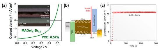
79]. The PCEs obtained so far with Ge-based perovskites in PSCs still lay below 1%, in particular 0.57% with MAGeI
2.7Br
0.3 [
80]; however, a PCS of 7.11% has been reported in a mixed Sn-Ge perovskite, CsSn
0.5Ge
0.5I
3, and the FTO/PCBM/perovskite/spiro-OMeTAD/Au device structure [
81] ().
Figure 9. (
a) SEM image of a FIB processed cross-section and J-V curve of an optimized MAGeI
2.7Br
0.3 based solar cell [
80] Reprinted with permission from Kopacic, I.; Friesenbichler, B.; Hoefler, S.F.; Kunert, B.; Plank, H.; Rath, T.; Trimmel, G.
ACS Appl. Energy Mater. 2018,
1, 343–347—Copyright 2018 American Chemical Society; (
b) energy-level diagram of the mixed Sn-Ge perovskite based device and (
c) stabilized power output of the Sn-Ge PSC [
81]. Reproduced with permission from Chen, M.; Ju, M.-G.; Garces, H.F.; Carl, A.D.; Ono, L.K.; Hawash, Z.; Zhang, Y.; Shen, T.; Qi, Y.; Grimm, R.L.; et al.
Nat. Commun. 2019,
10, 16—Copyright 2019 Springer Nature.
Bismuth materials (Bi), with the structure of A
3Bi
2X
9 have also drawn significant attention as non-toxic substitutes for Pb, because of their similar electronic configuration, very close ionic radius of 103 pm (Pb = 119 pm) and a good value of electronegativity. They typically consist of A cations of MA
+, Cs
+, Rb
+, K
+, guanidinium, cyclohexylammonium or imidazolium to form a 0D perovskite structure [
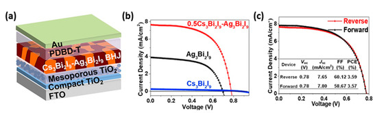
82]. The highest PCE recorder so far is of the order of 3.59%, in a Cs
3Bi
2I
9–Ag
3Bi
2I
9 bulk heterojunction (BHJ) perovskite solar cell ().
Figure 10. (
a) Schematic structure of FTO/c-TiO
2/mp-TiO
2/photoactive film/PDBD-T/Au device; (
b) J-V curves of the champion devices based on different photoactive films; (
c) J-V curves of the devices based on 0.5Cs
3Bi
2I
9-Ag
3Bi
2I
9 blend films [
83]. Adapted with permission—Copyright 2020 Elsevier.
Following Bi, antimony (Sb) based perovskites have been evaluated as photoactive materials, since they also exhibit appropriate optoelectronic properties to qualify as efficient absorbers for PSCs. They have the general structure of A
3Sb
2X
9, A being an organic or inorganic cation and X a halogen, while the cation and anion species combination determines the structure and dimensions. The antimony cation has a similar valence electronic configuration with Pb, even though it appears in a trivalent state; therefore, it might exhibit long carrier lifetimes. When incorporated in PSCs, Sb-based perovskites have so far achieved low PCEs, the highest being 3.34%, in a FTO/TiO
2/perovskite/spiro-OMeTAD/Au device configuration, using the MA
3Sb
2I
9−xCl
x perovskite. The PSCs retain 90% of the initial PCE after being stored under ambient conditions for over 1400 h and additionally, semitransparent Sb-based PSCs have been demonstrated with PCEs from 2.62 to 3.06% indicating the great potential for building integrated applications [
84] ().
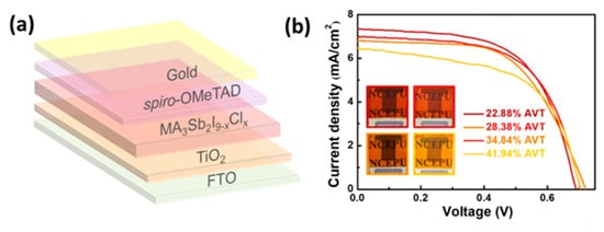
Figure 11. (
a) Schematic drawing of the semitransparent device architecture of glass/FTO/c-TiO
2/m-TiO
2/MA
3Sb
2I
9−xCl
x/spiro-OMeTAD/Au; (
b) J−V curves of the semitransparent PSCs with different full-device AVTs, obtained using ∼20 nm Au electrodes. The insets are photographs of the as-fabricated semitransparent PSCs (Reprinted with permission from Yang, Y.; Liu, C.; Cai, M.; Liao, Y.; Ding, Y.; Ma, S.; Liu, X.; Guli, M.; Dai, S.; Nazeeruddin, M.K.
ACS Appl. Mater. Interfaces 2020,
12, 17062–17069, Copyright 2020, American Chemical Society) [
84].
Finally, copper (Cu), has also emerged as promising for photovoltaic applications. Because of the small ionic radius (73 pm), layered 2D perovskite structures can be formed, with general formula (RNH
3)
2CuX
4 where RNH
3+ is an aliphatic or aromatic cation and X is a halogen. The highest PCE obtained so far is 2.41%, in a FTO/TiO
2/perovskite /Spiro-OMeTAD/Au device configuration and (CH
3NH
3)
2CuCl
4 perovskite [
85] ().
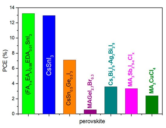
Figure 12. Summary of the highest reported PCE of Pb-free perovskites applied in PSCs with metal back contact.
This entry is adapted from the peer-reviewed paper 10.3390/electronics10101145