Some calculations estimate that the total amount of solar radiation received over a few hours would be sufficient for the planet’s energy consumption for 1 year. For many years, systems have been developed to improve the capture processes of this solar energy. Much of the difficulty stems from the need to cover large areas in order to capture radiation, and also from the fact that solar radiation is highly dependent on the geographic region.
Recent advances in the development of more efficient semiconductors have improved the efficiency of some systems to values of around 20%. However, we are still far from values that really are a real advantage to the use of fossil fuels. Over the past few decades, tremendous strides have been made in the development and improvement of photovoltaic systems, photoelectrochemical cells, and solar hydrogen production, although we are still far from the fact that these processes may represent the first option for the planet.
3.1.1. Photovoltaic Cells
Sunlight represents the most abundant renewable source of clean energy uninterruptedly available almost at any place in the globe. This resource can be utilized for various purposes which range from heating water to producing electricity through the use of photovoltaic (PV) technologies. Harvesting this incoming energy represents one of the most promising and hardly researched topics for chemists and physicists as it represents a green approach to produce energy from a source considered to be infinite. In addition, the relevant advantage of this approach over other new clean energy technologies is that sunlight can be directly converted into solar energy through solar cells. This technology offers a method to produce electrical energy in a cost-effective way avoiding the production of toxic materials as byproduct. Therefore, it stands as a pioneer within the green approaches available so far. It is expected that within the next seven years PV technologies will deliver approximately a range between 345 GW and 1081 GW and by 2050 the world energetic requirements will build up to approximately 30 TW. It is suggested that at least 20% of that necessity will be fulfilled by PV-based technologies [
63].
A photovoltaic cell is a device capable to harvest solar light and further convert it into electricity. Such device is composed of semiconductor materials, among which various 1-D nanomaterials are employed within the system [
64]. In brief, the main mechanism starts when the photons from sunlight are absorbed by the semiconductor, generating electrons and creating electron holes (h
+), which are subsequently filled by other electrons resulting from the same process happening in a cascade effect in adjacent molecules. As consequence, an electron flow along the material is produced. Such an effect is known as the photovoltaic effect, and PV devices work directing these flows in a specific direction, resulting in an electrical current [
65].
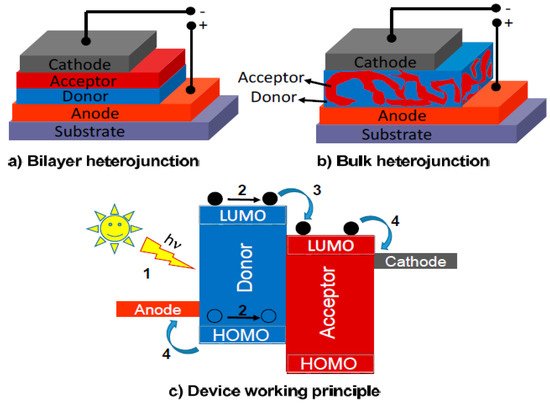
The PV device is made of a sandwich-like stack of n-type and p-type semiconductors joined by a n-p junction where the charge separation takes place. Herein, upon light incidence, the p-type semiconductor undergoes a charge separation producing a surplus of h
+ in the valence band. These h
+ reach the system anode. This material is the electron donor. Simultaneously, the n-type semiconductor makes the role of electron acceptor and therefore the electrons flux flows through the material to finally reach the system cathode. A very illustrative way to visualize how this system works is thinking of the stacked layers, as presented in [
64]. The h
+ will migrate to the anode like an air bubble emerging from a water body, whereas the electrons being transferred at the n-p junction interphase to the acceptor can be visualized as drops of water falling. A very important aspect to take into account is that a charge separation occurs when impacting with the material and, therefore, the system depends on two main factors: the absorption efficiency of the material, which in fact is related to the capacity that has the material to absorb photons efficiently, and the optimal charge separation. Whenever charge separation occurs, these species are called excitons and describe the promotion of electrons from the valence band to the electron band of a semiconductor. Moreover, if the recombination rate increases, the cell efficiency will decrease [
66,
67,
68].
Figure 1. Device structures (
a,
b); and basic photovoltaic effect process (
c). Reprinted with permission from reference [
64].
The PV effect previously described was first reported by Alexandre-Edmond Becquerel in 1839 [
69] while studying the effect of light on electrolytic cells. Nonetheless, it was only until more than 100 years later when the first modern Si solar cell was assembled by Russel Ohl [
69]. Furthermore, the energy crisis of the 1970s stimulated the development of this technology.
Current solar cell devices present significant challenges for their technological improvement. Speaking strictly of PV cells (PVCs), such devices in its common configurations are brittle, and generally with a low flexibility. Therefore, their projection for use in industries such as textiles, for wearable application seems challenging. The scientific community, nonetheless, started to propose 1D materials as a means to include a flexible component to these devices that has not been considered until 2001 [
70]. This development was closely followed by the implementation of 1D polymer solar cells in coaxial configurations onto optical fibers [
71]. Moreover, in 2008 a testing approach was proposed instead of a coaxial path to reach the same aim [
72]. From then on, different materials have been tested, looking to improve harvesting efficiencies, energy densities, and the obtention of more lightweight devices. Such approaches, materials, and results will be discussed throughout the rest of this section.
The implementation of 1D materials for energy harvesting has been achieved by using coaxial structures [
73] (see ). Polymorphic core/multishell NWs exhibit excellent photovoltaic properties, enhancing absorption in different regions of the solar spectrum, for the development of next-generation, ultrathin solar cells. Other examples of coaxial structures are composed of a core-shell architecture with a fiber electrode core, another electrode coating the whole system, and an active material sandwiched in-between [
74] (see ).
Figure 2. Three-dimensional schematic of a core/shell NW and cross-sectional schematics of four core/shell diode geometries, and SEM image of an as-grown, core/shell p/in Si NW, scale bar = 100 nm (
a), and TEM image of a NW cross-section showing a core surrounded by crystalline shell, scale bar = 50 nm (
b). Reprinted with permission from reference [
73].
Figure 3. General scheme of a photovoltaic fiber with an active material sandwiched in between two electrodes, for the assembly of an FSC. Side view (
a) and cross-sectional view (
b) Reprinted with permission from reference [
74].
Typically, the semiconductor layer is composed either of TiO
2 or ZnO nanostructures, the photoactive material (dye) and the counter electrode shell (conducting polymer or carbonaceous material). Such devices have been named as Fiber Solar Cells (FSCs), when intended for PV uses. FSCs have been proposed following two different charge transport mechanisms, photochemical and solid-state transport. For the purpose of this review, it will only be discussed photochemical transportation. In-depth solid-state transport PV materials can be found elsewhere [
74]. One, is based on a photoelectrochemical transport mechanism consisting of a dye sensitized TiO
2 nanoparticles (NPs) or nanotubes (NTs) [
75,
76,
77], commonly referred to as dye-sensitized solar cells (DSSC). Yang et al. [
78], for instance, reported an approach to produce stretchable fibers initially intended for photovoltaic technologies applied onto textile technologies, with efficiencies up to 7.13%. Herein, the fibers were initially created by winding multi walled carbon nanotubes (MWCNTs), synthesized by chemical vapor deposition (CVD) onto rubber fibers [
79] following an angle α of coating ranging from 60° to 75° as the optimal values to keep the mechanical properties of the material stable, while gaining resistance thereof (0.27 to 2.4 kΩ/cm when passing from 15° to 75°). These resistances can be reduced by increasing the fiber sheath. Similarly, approaches for the fabrication of FSCs have been reported using semiconducting nanowire arrays such as CdSe [
80,
81], and quantum dot-sensitized ZnO nanowires [
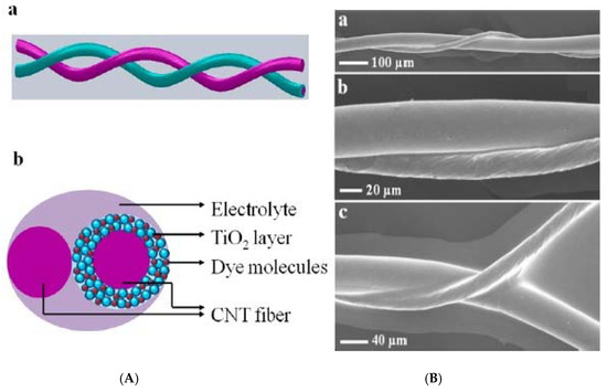
82]. Twisted structures represent the second structure used in FSCs (see ). Herein, the fiber photoanode is deposited with a semiconductor layer and further coated with a dye is wound with a fiber counter electrode [
72]. Specifically, Chen et al. [
83], described a system where CNT fibers dye-loaded with TiO
2 NPs, as the working electrode and another CNT fiber used as the counter electrode were developed as FSCs. The CNT/TiO
2 fibers were prepared by repeatedly dipping the CNT fiber into a TiO
2 colloidal solution followed by sintering at 500 °C for 60 min. Authors attributed the high TiO
2 NPs adsorption onto the CNT in part to the high surface area of the fiber, reaching particle thicknesses ranging from 4 to 30 µm, depending on the dipping times. This device reached an efficiency of 2.94%.
Figure 4. (
A) Schematic representation of a wire-shaped FSC formed by two CNTs (one coated with TiO
2NPs/dye; the other in its bare state) in a twisted configuration. (
B) The SEM characterization of the system at different magnifications. Reprinted with permission from reference [
83].
Among the most relevant favorable points to exalt from these two structures of FSCs, one can mention the high flexibility reachable by following methods as those described above. Interestingly, this flexibility allows the curves of current density as a function of voltage for the twisted architecture remains close to unchanged after bending [
84].
In other modifications used to improve both the efficiency and robustness of these cells, the implementation of noble metals in junction with carbonaceous materials have been reported. For instance, MWCNTs have been dispersed and mixed with Fe
3O
4 or Ni NPs to reach hybrid FSCs, with efficiencies of 16.6% for the fibers coated with Fe
3O
4 and 11.2% for fibers with Ni NPs [
85].
As we delve deeper into further considerations to improve the performance of PVCs limited to 1D materials, the power efficiency becomes a critical aspect to look upon, as it guarantees an acceptable output of electric power. To meet this aim, it is necessary to develop materials with good mechanical, electrical, and chemical properties [
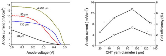
73]. For instance, the incorporation of Pt NPs to a carbonaceous material (e.g., CNTs) has been proposed as the counter electrode of titanium nanowires, with enhanced Pt-electrolyte interfacial area and a reduced charge-transfer resistance. Zhang et al. [
86], reported the fabrication of TiO
2-based dye sensitized fiber solar cells with a Pt- CNT yarns, yielding a considerable shift in current and voltage depending on the yarn diameter. The higher increase in current density (from 5.22 to 13.52 mA/cm
2) occurred in a diameter range of 20–90 µm, with a cell efficiency change from 0.49 % to 3.38 %. However, beyond these wire dimensions, the current dropped to approximately 8 mA/cm
2, with an efficiency of 200%. shows the improvement of current density as a function of yarn diameter and its corresponding cell efficiency.
Figure 5. The anode current as a function of the Pt-CNT yarn diameter (
left), and the corresponding fiber solar cells efficiency
(right). Adapted from Zhang et al. 2012. Reproduced with permission from reference [
86].
The noble metal chosen as fiber electrode, must ensure proper conductivity. Among the most common materials employed, Ti [
84,
85,
86], Al [
87], and stainless-steel wires [
72] stand out. Nonetheless, the implementation of materials with higher electrochemical activities such as Pt with improved methods to rough their surfaces will determine future improvements in these systems as it will enhance the further interaction of the carbonaceous materials used in these devices [
73].
Electrospun nanofibers have also been applied to dye solar sensitive cells [
88], specifically combining them with metallic compounds, giving rise to systems with high efficiency and stability. Chemical composition, shape, and other properties can be easily controlled by adjusting key parameters during synthesis, which has enabled the development of electrode materials for solar cells and more recently to manufacture bulk organic heterojunction solar cells and perovskite solar cells [
89].
Finally, it is necessary to mention 1D perovskite NWs. Growing these materials in a low dimensional manner was first proposed as a vapor-liquid-solid growth, which enabled the growth of anisotropic perovskite NWs [
90]. In this approach, a catalytic nanodroplet of a eutectic liquid alloy adsorbs the precursor in its vapor state. Furthermore, inducing a 1D anisotropic growth in the liquid-solid interphase between the crystalline material and the semiconductor [
91]. Perovskites represent a material of great interest due to specific properties, such as the fact that these materials have more “softer“ crystalline lattices if compared to other semiconductors, which enables a fast crystal formation unlike other crystalline materials [
92]. Moreover, various approaches can be taken to come around the production of 1D perovskites such as solution phase recrystallization growth processing [
93], the vapor phase conversion method [
94], direct vapor-phase growth [
95], colloidal nanowire synthesis [
96], space confined nanowire growth [
97], nanowire growth via intermediate adducts [
98], ion exchange of existing perovskite NWs [
99], and NW heterostructures [
100].
3.1.2. Photochemical Cells
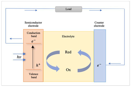
A photoelectrochemical cell converts light to electric power leaving no net chemical change behind [
101] (see ). Photons of energy exceeding that of the band gap generate electron–hole pairs and the negative charge carriers move through the bulk of the semiconductor to the current collector and the external circuit [
101]. The positive holes are driven to the surface where they are scavenged by the reduced form of the redox relay molecule (R), oxidizing it to O by the following reaction: h
+ + R → O [
101]. The oxidized form O is reduced back to R by the electrons that re-enter the cell from the external circuit [
101]. In the following, some interesting examples of 1-dimensional nanomaterials used for photoelectrochemical cell applications are described.
Figure 6. Schematic of a photoelectrochemical cell.
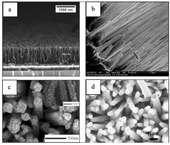
1–D morphologies () have shown progress when it comes to energy applications in the last five years [
102,
103,
104,
105]. For instance, it has been shown that Bi
2O
3/BiAl oxides nanowires (NWs) arrays () enhance PEC’s performance showing a hydrogen generation of up to 696 μmol cm
−2, which corresponds to a Faradaic efficiency of 93% [
102]. CuO NWs photocathodes fabricated via hydrothermal method have also shown a photocurrent of ~1.4 mA cm
-2 at 0 V vs. RHE under AM 1.5G irradiation, which is one of the highest photocurrents based on bare CuO photocathode [
103]. Hydrogenated TiO
2/ZnO heterojunction nanorod arrays for PEC energy applications have shown photocurrent densities of nearly 2.5 mA cm
−2, demonstrating a promising candidate for PEC cells [
104]. Gold (Au) nanoparticles decorated highly ordered ZnO/CdS nanotube arrays (ZnO/CdS/Au NTAs) photoanodes exhibits a photocurrent density of 21.53 mA/cm
2 at 1.2 V vs. Ag/AgCl and 3.45% photoconversion efficiency (PCE) among the parallel photoanodes under visible light illumination (λ > 420 nm) [
105].
Figure 7. SEM characterization of (
a) Bi:Al 21:1 photocathode [
100], (
b) CuO NWs [
101], (
c) Hydrogenated TiO
2/ZnO heterojunction (TZ10-H) [
102], and (
d) ZnO/CdS/Au NTAs [
103]. Reproduced with permission from references [
102,
103,
104,
105].
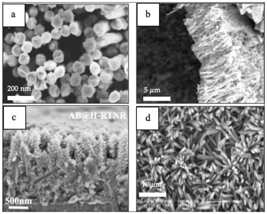
1–D materials () have also been integrated in PEC cells for sensing applications [
106,
107,
108,
109]. For instance, Au–NiO
1−x (0 < x < 1) hybrid NWs arrays are used as glucose sensors that exhibits an ultrahigh sensitivity of 4.061 mA cm
−2 mM
−1, low detection limit and a wide level of glucose concentration in the detection range of 0.005–15 mM in PEC cells [
106]. In addition, TiO
2 NWs prepared by template sol-gel synthesis are practical for a hydrazine photoelectrochemical sensor having a limit of detection (LOD) of 1.91 μM and a limit of quantification (LOQ) 8.91mM [
107]. Nanorods such as high-performance anatase-branch@hydrogenated rutile-nanorod TiO
2 have also been used for detecting chemical oxygen demand (COD) in wastewater [
108]. Featuring a detection limit of 0.2 ppm and a wide linear detection range of 1.25–576 ppm [
108]. A propyl gallate PEC sensor based on ZnO nanorods and MoS
2 flakes showed a wide linear range from 1.25 10
−7 to 1.47 10
−3 mol L
−1 with a detection limit as low as 1.2 10
−8 mol L
−1 [
109].
Figure 8. (
a) Au–NiO
1−x (0 < x < 1) hybrid nanowire arrays [
106], (
b) TiO
2 nanowires [
107], (
c) anatase-branch@hydrogenated rutile nanorod TiO
2 [
108], (
d) ZnO nanorods and MoS
2 flakes [
109]. Reproduced with permission from references [
106,
107,
108,
109].
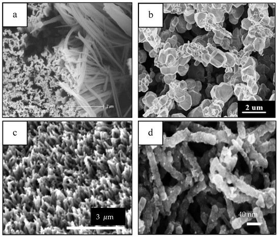
In addition, 1–D materials can also be used in PECs for other applications [
110,
111,
112,
113] (see ). A photoelectrocatalytic microbial fuel cell (photo-MFC), consisting of a palladium (Pd) NPs-modified p-type silicon (Si) NW photocathode used to degrade methyl orange (MO), and to generate electricity simultaneously exhibited a MO removal efficiency of 84.5% and maximum output power density of 0.119 W/m
2 within 36 h [
110]. A WO
3 NFs-C/Cu
2O NWAs visible-light response dual-photoelectrode solar-charged photoelectrochemical wastewater fuel cell (scPEWFC) was constructed for efficient hydrogen production based on the promotion of phenol oxidation at the anode [
111]. The hydrogen production reaches as high as 93.08 μmol cm
-2 by the photoelectrocatalytic oxidation of phenol (total organic carbon (TOC) removal rate reached 82.12%) of WO
3 NFs-C/Cu
2O NWAs under visible light irradiation for 8 h without additional bias, which is 3.02 times higher than that of pure photocatalytic water splitting [
111]. A microbial photoelectrochemical cell (MPEC) with a p-type Co
3O
4 nanorod-arrayed photocathode for CO
2 conversion to formic acid [
112]. The yield of formic acid produced by this MPEC under visible light irradiation was 239 ± 10 μmol in 10 h and the maximum power density was 331 ± 4 mW m
−2 under visible light [
112]. In 2015, scientists developed a novel nanostructured plasmonic Ag/AgCl @ chiral TiO
2 nanofibers (Ag and AgCl NPs supported on chiral TiO
2 nanofibers) photoanode to treat urban wastewaters with simultaneous hydrogen production [
113]. The electrolyte in the dye-sensitized solar cell (DSSC) was actual wastewater with added estrogen (17-β-ethynyl estradiol, EE2) and a heavy metal (Cu
2+) [
113]. Almost total removal of carbon (TOC), Cu
2+, EE2, and 70% removal of total nitrogen (TN) were achieved under visible-light irradiation [
113]. A relatively high solar energy conversion efficiency (PCE 3.09%) was recorded and approximately 98% of the electricity was converted to H
2 after the consumption of dissolved oxygen (DO), Cu
2+ and TN [
113].
Figure 9. (
a) Si nanowires [
110], (
b) C/Cu
2O NWAs [
111], (
c) Co
3O
4 nanorods [
112], and (
d) Ag/AgCl @ chiral TiO
2 nanofibers [
113]. Reproduced with permission from references [
110,
111,
112,
113].
In conclusion, 1–D morphologies have been used in various PEC’s applications ranging from hydrogen production and sensors to even degradation of pollutants in the last five years. They have been shown to enhance performance, used for electrode stabilization, as support materials and even in conjunction with biological organisms in the case of photo-MFC. The work presented in this section proves that 1–D morphologies can adapt various roles when it comes to PEC applications, making these materials excellent candidates for multi-purpose applications given by their versatility, ease of modification, as well as their many benefits that comes from their composition characteristics.
3.2. Piezoelectric and Thermoelectric Materials
Piezoelectric effect is the ability of some materials to produce an electrical charge in response to applied mechanical stress. This effect is reversible, and also includes the opposite behavior, that is, the generation of mechanical stress when an electric field is applied to the material. Since the first nanomaterials capable of showing this effect were reported, various high-performance materials have been developed with interesting applications from an energy point of view. ZnO nanowires (ZnO NWs) are characterized by a hexagonal structure with significant anisotropy along the c axis, and perpendicular to it, so the application of stresses on this material gives rise to a piezoelectric effect [
149,
150,
151]. When the curvature of the material is caused, a displacement of the cations and anions that form the nanowire structure takes place, which causes the appearance of a dipole that, macroscopically, will cause the appearance of an electrical potential.
In general, this effect can be observed in certain nanowires and nanobelts because, in this conformation, the materials can withstand great mechanical stresses. These materials include those based on ZnO, GaN, InN, CdTe, CdSe, and others, with really high efficiencies for practical purposes (i.e., 0.4V in ZnO [
150], 0.35V in GaN [
152], 0.3 V in CdTe [
153], 60 mV in InN [
154], or 137 mV in CdSe [
155]. Of these materials, ZnO is by far the easiest to obtain; it is eco-friendly with the environment, and the synthesis of large quantities can be obtained efficiently and at low temperature [
150]. Other materials with large piezoelectric coefficients include some ferroelectric nanowires such as Pb(Zr,Ti)O
3 [
156], and BaTiO
3 [
157]. Xu et al. [
158] reported high output voltages for Pb(Zr,Ti)O
3, with values as high as 0.7 V. In the case of BaTiO
3 nanotubes, with perovskite structure, output voltages of up to 5.5 V have been obtained, under a stress of 1 MPa [
159]. When this material is synthesized in the form of thin films by rf magnetron, the output voltages are certainly lower, with values that can reach 1V. Other interesting materials capable of presenting a high piezoelectric response are represented by composites. One of them is the NaNbO
3 nanowire PDMS polymer composite, with which up to 3.2 V has been obtained. Of all the materials described so far, vertically aligned Pb(Zr
0.52Ti
0.48)O
3 nanowires with an output voltage of 209 V are one of the most efficient systems.
In contrast to the piezoelectric materials described above, capable of generating a voltage when subjected to mechanical stresses, there are some materials capable of converting temperature differences to electricity and vice versa. If we consider that the vast majority of energy consumption processes waste more than half of this in the form of heat, there is no doubt that having systems capable of transforming this heat into reusable energy would be very advantageous. Thermoelectricity is based on the Seebeck-effect, and is due to the different Fermi electron distribution as a function of temperature. Although this effect was initially observed in bimetal junctions, thermoelectric materials are now generally based on semiconductor alloys of Co, Bi, Te, Pb, or Sr. The process implies that a temperature difference occurs between the connected ends of p-type and n-type semiconductors, causing the free carriers to diffuse from the hot side to the cold side, generating a potential difference between both ends. Traditionally, 1D materials capable of exhibiting this effect have been dominated by bismuth. This semimetal, when found with low dimensionality, as in the case of nanowires, is characterized by a band structure and an appropriate electron distribution to show these effects [
160].
The basic property of the material that governs the efficiency of thermoelectric generators is the Figure of thermoelectric merit, defined as Z = S
2σ / κ, where S is the Seebeck coefficient, or thermoelectric power, and σ and κ are the electrical and thermal conductivity, respectively [
161]. Z is generally multiplied by the average temperature T to produce a number ZT, which is the parameter used to determine the efficiency of the material. The most advanced thermoelectric materials show a ZT > 3. In order to achieve this, the material is required to have high electrical conductivity (σ), and low thermal conductivity (κ), which is not obvious. One way to achieve materials with this double behavior is through the use of 1D-composites [
162]. In this sense, 1D organic composites have recently been developed with significant improvements. Among these, we can mention poly(3,4-ethylenedioxythiophene): p-toluenesulfonic acid (PEDOT: p-TSA), which is synthesized on glass fiber. In this material, and after post-processing, S and especially σ experienced a significant increase, with a substantial improvement in behavior [
163]. Other nanostructured organic materials based on carbon nanotubes have shown power factors (PF) of up to 95 [
164]. Materials based on PbTe-modified PEDOT nanotubes have also shown high values of S, although in these cases the electrical conductivity is low [
165]. Perhaps, future developments of thermoelectric materials will mainly include conductive polymers, whose doping will make it possible to control impurities and defects in the material, allowing to effectively regulate the carrier mobility.
3.3. Electrochemical Energy Storage
3.3.1. Batteries
Among the battery systems available today, rechargeable lithium ion batteries (LIBs) are the most common and the ones with higher commercial importance due to their outstanding energy density. However, state-of art LIBs are approaching their energy density boundary and new materials and structures are being developed to push this boundary further and meet the ever-increasing energy storage demand.
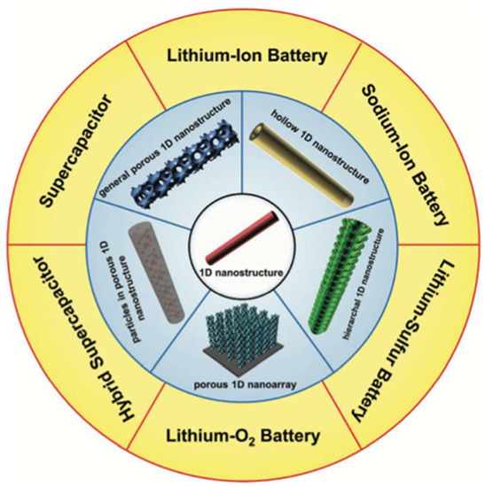
Batteries are usually characterized by high energy density but mediocre power density. Their limitations come from the energy storage mechanism, which is based on redox reactions that takes place in the volume of the electrode material. The incorporation of the metal ions into the bulk of the material requires the diffusion of the latter from the electrolyte to the reaction site, which is a process usually slow. This is the root of the low power density and there is currently a great effort being made to improve it. In this aspect, nanomaterials, and specifically 1D nanomaterials, are a big asset. Their high surface to volume ratio reduces the diffusion distances while their high aspect ratio assures good long-range conduction, dramatically improving their charge/discharge rates [
166,
167,
168] (see ).
Figure 30. Porous 1D nanostructures and potential applications in electrochemical energy storage. Reprinted with permission from reference [
166].
Another important issue for the batteries is cycle performance. High capacity materials tend to be mechanically unstable upon cycling because of the expansion and shrinking produced during the accommodation of the metal ions. This mechanical stress induces the pulverization of the active material which impacts the battery life by the loss of contact of the crumbled pieces. In this regard, the nano scale can also help to improve the stability of the materials, reducing the degradation by buffering the size changes and therefore increasing the lifetime of the devices [
169,
170].
A number of other benefits can also be ascribed to the 1D nanomaterials in LIBs, such as good flexibility compared to 2D and 3D nanomaterials [
171,
172,
173], the capability to create porous or hollow structures [
166], or the possibility to create more complex structures that can easily be grown on thin films to form flexible, self-standing energy storage devices [
173,
174].
One dimensional materials can be present in the LIBs fulfilling two different functions: as an active material or as a conductive material. The advantages and representative examples of 1D materials in both functionalities in LIBs are summarized in the following points.
One Dimensional Active Material
One dimensional nanostructures have recently received a significant attention in respect of their application in batteries. The advantages above mentioned have contributed to the development of an extensive variety of nanostructures (nanorods, nanowires, nanotubes, etc) for even a wider range of materials. gives a brief outlook of the variety and diversity of the materials and structures demonstrated in the literature.
Table 1. Examples of different 1D battery nanomaterials by structure and storage mechanism.
| Nanorods |
Nanowires |
Nanotubes |
Nanocables |
| 3 ZnMnO3 [197] |
2 Si [170] |
1 g-CNTs [179] |
2 Cu-Si [198] |
950 mAh/g (0.5 A/g)
500 cycles |
1200 mAh/g (2 A/g)
500 cycles |
200 mAh/g (0.5 A/g)
400 cycles |
1500 mAh/g (1.4 A/g)
100 cycles |
| 3 ZnCo2O4 [199] |
2 Si [200] |
3 Co3O4 [201] |
1,2 SnO2-TiO2 [202] |
1050 mAh/g (0.4 A/g)
200 cycles |
900 mAh/g (0.2 C)
100 cycles |
1800 mAh/g (0.3 A/g)
100 cycles |
300 mAh/g (0.1 C)
50 cycles |
| 2 β-Sn [203] |
1 TiO2 [52] |
3 ZnMn2O4 [204] |
3 CNT@Fe3O4@C [205] |
600 mAh/g (0.2 C)
100 cycles |
350 mAh/g (0.02 A/g)
35 cycles |
670 mAh/g (0.2 A/g)
280 cycles |
700 mAh/g (2 A/g)
200 cycles |
| 3 α-Fe2O3 [206] |
2 Ge [207] |
2,3 SnO2-CuO [208] |
1 MWNT@LTO [209] |
970 mAh/g (0.5 C)
100 cycles |
900 mAh/g (0.5 C)
1100 cycles |
600 mAh/g (0.5 A/g)
100 cycles |
130 mAh/g (10 C)
100 cycles |
| 3 CuO [210] |
2,3 Zn2GeO4 [211] |
2 Si [212] |
2 Ni-Si [213] |
670 mAh/g (0.1 A/g)
150 cycles |
1200 mAh/g (0.1 C)
100 cycles |
600 mAh/g (12 C)
6000 cycles |
1100 mAh/g (0.5 C)
100 cycles |
| 3 V2O3 [214] |
3 WO3 [215] |
3 Zn4Sb3 [216] |
2,3 Ag@γ-Fe2O3 [217] |
200 mAh/g (0.1 C)
125 cycles |
660 mAh/g (0.28 C)
140 cycles |
450 mAh/g (0.1 A/g)
100 cycles |
890 mAh/g (0.1 C)
60 cycles |
In addition to the material and the shape it is presented, the electrode fabrication has also a very decisive importance in nanomaterials. Some of the most attractive properties of the 1D materials are only fully exploited in certain electrode configurations. In particular, the growth of aligned 1D nanostructures on conductive substrates, maximize the exposed surface, providing an efficient electron transfer, deep electrolyte penetration, and good strain accommodation [
175,
176].
On the other hand, a wide variety of 1D nanomaterials have been developed as active material in LIBs electrodes as a component of the slurry paste (in combination with conductive additives and binders), or fabricating freestanding electrodes. In this case, the key to achieve good electrochemical performances is usually related with the proper arrangement of the materials inside the electrode and the smart combination with other synergetic nanomaterials [
52,
177].
The active materials for LIBs can be divided into three main groups based on their reaction mechanisms: (1) intercalation, (2) alloying, and (3) conversion. In all of them, 1D materials have been used and a clear performance improvement was accomplished.
Intercalation is the most common of the lithiation processes in batteries. During this process metal ions are inserted in the outer of the layered materials structure, producing minimal structural changes and therefore provides a stable cycling performance [
178]. In opposition to their stability, their capacity is generally low which handicaps their energy density. Carbon materials, titanium dioxide and spinel lithium titanate (Li
4Ti
5O
12, LTO) are the most representative anode materials based on this mechanism. Among the carbon materials, carbon nanotubes (CNTs) have gained huge interest due to the unique structural, electrical, mechanical and electronic properties. In CNTs, Li
+ has double space to incorporate (inner and outer surfaces) and its flexible morphology offers a stable capacity without pulverization in the electrode [
179].
The 1D morphology of nanowires is particularly beneficial to maintaining firm electronic contacts with the conductive agents during charge/discharge cycles. Thus, TiO
2-based nanowires, nanorods, nanotubes and nanofibers [
180,
181,
182,
183,
184] have been fabricated, exhibiting excellent high-rate cycling performance.
LTO is a highly appealing anode materials for LIBs due to its extraordinary cycling performance and high safety. Yet, its low conductivity and moderate Li
+ diffusion coefficient limits its rate capability, and its capacity is even lower than that of the graphite. Still, the 1D nano-structural LTO (a nanorod material (NT-LTO/C) formed by a molecular self-assembly has proven to be a good strategy to improve the properties of the material, shortening the transport lengths, and thereby improving the rate performance [
185] of nanorod material (NT-LTO/C) by a novel in situ molecular self-assembly strategy.
Some materials can electrochemically form Lithium alloys in a reversible way. These alloying materials are characterized by high specific capacities and safe operating potentials. While the specific capacity of the alloy based anodes like Si (4200 mAh g
−1), Ge (1600 mAh g
−1), Sn (994 mAh g
−1), etc., are more than graphite (372 mAh g
−1), the poor cycling stability and the irreversible capacities at the initial cycles limit their practical applications [
186,
187]. These effects arise from the swelling/shrinking during lithiation/de-lithiation, reaching volume changes up to 400%, which results in pulverization of the active materials and lose of electrical contact. To overcome these inherent limitations, it has been proven that 1D nanostructures help to release the stress without breaking which helps to retain the capacity [
188,
189].
A wide selection of 1D nanomaterials have been used as LIBs alloy anodes [
190,
191] and comparatively, their electrochemical performance has been shown to be significantly improved compared to the same material in different morphologies. Some examples are displayed in .
At the turn of the 21st century, new perspectives for the development of LIBs brought interest in the search of a new concept of reactivity with Li, different from those of intercalation and alloy with Li. These circumstances encouraged the investigation of materials with new functional mechanisms; those can make the reactions of "conversion" with lithium. The reversible electrochemical reaction of lithium with transition metal oxides or sulfides, conventionally called the "conversion reaction" [
192].
Through this multi-electron transfer process, conversion-type materials can easily accommodate more Li ions to achieve high specific capacities. Conversion type materials such as transition metal oxides (TMOs) have become a promising alternative to graphite due to their safety, low cost and the high theoretical specific capacity. However, the use of these conversion materials also has its drawbacks, such as low conductivity, low initial coulomb efficiency, instability during long cycling, and high-volume expansion, which limit their application in LIBs. Some of these limitations that can be overcome using nanostructures, such as 1D metal nanostructure arrays oxides, sulphides, and hybrid structures, as shown in .
One Dimensional Conductive Agent
One of the most common drawbacks of nanomaterials is their low conductivity and poor connection with the conductive network composing the electrode [
193,
194]. Regarding these limitations, an approach that has become popular lately is the use of carbon nanotubes (CNTs) and nanofibers (CNFs) [
195,
196]. As opposition to other conductive agents, lD conductive materials keeps long range of interconnection of active material particles, while maintaining high porosity and allowing the electrolyte to penetrate deeper into the electrode.
The 1D carbon nanostructures cannot only provide better electrical connection to the active materials, but also their porous structures are beneficial allowing the accommodation of the volume expansion [
179,
195]. Furthermore, 1D carbon nanomaterials provide good mechanical robustness and flexibility to the electrodes due to their excellent mechanical properties.
In addition, the good interconnection that they provide, it allows a much lower weight than other additives, further enhancing the energy density of the electrodes. This approach is quite mature, and it has become a standard for the battery manufacturers, being currently applied by OCSiAl (carbon nanotube manufacturer) in partnership with Shenzhen BAK Power Battery (China), Haiyi Enterprise (China), and Polaris Battery Labs (USA).
