Your browser does not fully support modern features. Please upgrade for a smoother experience.
Please note this is an old version of this entry, which may differ significantly from the current revision.
Subjects:
Materials Science, Coatings & Films
The properties of molybdenum disulfide (MoS2), such as direct band gap transition in low dimensional structures, strong light–matter interaction and good carrier mobility, combined with the possibility of fabricating thin MoS2 films, have attracted interest for this material in the field of optoelectronics.
- MoS2
- TMD
- photodetector
- heterostructure
- thin film
1. Introduction
Recent improvements in optoelectronics have been partly focused on the use of two-dimensional materials to produce photodetectors. The possibility of fabricating very thin optoelectronic devices, having high performance, low production costs and mechanical flexibility has been emerging in the last decade. Graphene was the first 2D material considered for photodetection applications, thanks to its outstanding electrical properties, in particular its impressive planar mobility, reaching 200,000 cm2/(V s), that allows to build photodetectors with bandwidth up to 40 GHz [1,2]. However, one of its mayor limitation for its use as photodetector active layer is the absence of an energy band gap, leading to high noise contribution to the signal, arising from dark currents.
Therefore, the investigation of 2D materials with finite bandgap has increased in recent years and transition metal dichalcogenides (TMDs) have aroused more and more interest. Despite the modest mobility reported for these materials, which can reach about 200 cm2/(V s) [3], TMDs possess interesting electro-optical properties. A transition from indirect to direct bandgap has been observed in TMDs by reducing the dimensions from the bulk material to the monolayer limit [4]. Moreover, a strong light–matter interaction is observed for 2D-TMDs, due to the direct band gap and to the strong excitonic nature of their low dimensional structures. For TMDs, absorbance values that are one order of magnitude higher than Si and GaAs are reported [5], thus providing strong light absorption with a very thin layer of the photoactive material. These features, combined with a higher mechanical flexibility of 2D-TMDs compared to their bulk structures, allow us to fabricate very thin photodetectors also based on flexible substrates, opening the possibility to realize flexible and wearable devices. Applications for such devices can be related to medicine, biosensing, optical communications and security.
Among the TMDs, molybdenum disulfide (MoS2) attracted much interest in the last decade, also due to the relative abundance of molybdenite in nature. MoS2 belongs to the family of the group VI transition metal dichalcogenides, where a layer of transition metal atoms (Mo, W) is sandwiched between two layers of chalcogen atoms (S, Se, Te) as depicted in Figure 1.
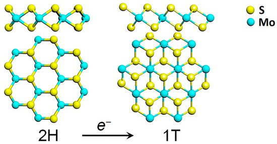
Figure 1. Transformation of the hexagonal 2H polymorph of MoS2 into its 1T phase, through electron transfer. Reprinted with permission from ref. [6]. © 2017 AIP Publishing.
Each MoS2 layer is generally stacked onto each other via weak van der Waals forces in an ABA stacking sequence, building a hexagonal structure (2H-TMD), which possesses a semiconducting behaviour. Another metastable phase of MoS2 is known, with a tetragonal symmetry (1T-MoS2) and ABC stacking sequence (Figure 1). The 1T phase of MoS2 is not stable at room temperature [7], but it can be induced by several processes such as chemical treatment [8], plasmonic hot electron transfer [9], electron beam irradiation [6,10], through charge transfer in the TMD lattice. A subsequent annealing process is then required to restore the 2H-MoS2 phase [6].
Bulk TMD electronic properties are dominated by indirect transition from the maximum of the valence band, located at the Γ point of the Brillouin zone, and the minimum of the conduction band [11,12,13]. For MoS2, the bulk electronic structure is characterized by an indirect energy band gap of about 1.2 eV [14]. As with other group VI TMDs, at the monolayer limit MoS2 modifies its energy band structure towards a direct electronic transition from the K and K’ points of the Brillouin zone, reaching an energy band gap of 1.8 eV [14,15]. This behaviour can be explained by an increase in the indirect band gap due to a considerable quantum confinement effect in the out-of-plane direction when the dimensions of the material are reduced to few layers. On the other hand, the direct transition remains unaffected, becoming the minimum energetic band-to-band transition [11,12,13] (Figure 2a). Moreover, TMDs are reported to have strong spin-orbit coupling (SOC), associated with the d-orbitals of transition metals [6,16,17]. The SOC breaks the degeneracy in the valence band, leading to two energetic maxima located at the K and K’ points, separated by an energy splitting of 160 meV for a monolayer MoS2 [16] (Figure 2b). This broken degeneracy opens for MoS2 the possibility for optoelectronic applications in the field of valleytronics [18,19].
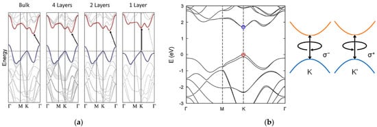
Figure 2. Energetic band structure of MoS2. (a) Transition from indirect to direct band gap moving from the bulk MoS2 to the single layer of MoS2. Reprinted with permission from ref. [15]. © 2010, American Chemical Society. (b) Degeneracy at the K point in the valence band of a single MoS2 layer. Reprinted with permission from ref. [6]. © 2017, AIP Publishing.
When MoS2 is irradiated with photon energies larger than its bandgap, photons are absorbed and electrons are promoted to the conduction band, leaving holes in the valence band. The optical absorption of visible light by MoS2 in the monolayer limit is dominated by the direct transition from the K and K’ points of the valence band. However, light absorption experiments show peculiar resonant features in 2D structures of MoS2 (Figure 3), that can be associated with its strong excitonic nature [4,15]. The experimentally observed absorption peaks at specific energies (EA = 1.88 eV, EB = 2.03 eV in the monolayer limit [20]) represent the excitonic energies of MoS2. The relative positions of the A and B peaks are related both to an increase in the SOC and to a reduction in the bandgap, approaching the bulk structure of MoS2 [20].
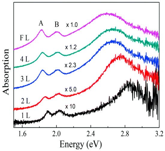
Figure 3. Absorption spectrum of MoS2 varying the number of layers from 1 layer (1L) to few layers (FL), where A and B represent the excitonic peaks of MoS2. Reprinted with permission from ref. [20]. 2014, Creative Commons Attribution 3.0 Unported Licence.
For these reasons, in 2D-MoS2, the bandgap measured with optical techniques turns out to be lower than the one measured with electronic techniques [6]. The strong light–matter interaction that characterizes MoS2 is reflected in a high absorption coefficient that can reach about 106/cm [21], which is at least one order of magnitude higher than standard semiconductors like Si and GaAs. Moreover, a single MoS2 layer is reported to absorb up to 10% of the sunlight [5]. This superior light absorption makes MoS2 suitable to build photodetectors based on very thin layers of material, still having high light conversion efficiency.
Therefore, the production of thin MoS2 films is a central step of the device fabrication and several approaches have been investigated so far. Thanks to the weak van der Waals interaction between MoS2 layers, it is possible to obtain mono- or few-layered structures by a simple mechanical exfoliation of bulk MoS2 [22]. This approach has been extensively used in many studies [23,24,25,26,27,28,29,30,31,32,33,34,35,36] for its intrinsic simplicity, but suffers from some critical issues. In fact, MoS2 mechanical exfoliation generally leads to very small flakes (lateral size < 10 um) [37] and it is a low yield process. Therefore, it is unsuitable for industrially scalable-applications [38]. Other synthesis methods have been investigated to overcome these critical aspects. Chemical vapour deposition (CVD) is a powerful bottom-up approach. This method is the most compatible with the existing semiconductor technology. In CVD, large area films with high uniformity can be grown directly on the substrate, through the chemical reactions involved in the process. Despite the high controllability of the process and the high uniformity that can be achieved, CVD has the limit of being a costly process and requires high temperatures (700–1000 °C), making the process less affordable and not suitable for deposition on flexible substrates. Moreover, in most of the CVD processes used to produce MoS2, one of the precursors involved is H2S, which is toxic. As an alternative to standard CVD, plasma-enhanced CVD (PECVD) has also been exploited in order to reduce the temperature needed for the reaction (150–300 °C), thus allowing film deposition also on plastic substrates [39].
Among the bottom-up approaches, wet chemical syntheses can also be exploited for the fabrication of large area MoS2 films on different substrates. MoS2 sols can be prepared both at ambient pressure or under hydrothermal [40] or solvothermal [41] synthesis conditions. The sols can be used for coating different substrates by spin-coating or dip-coating. Generally, an annealing process (at 500–800 °C) is required in order to improve the crystallinity of the sample and an additional sulphurisation step is needed. Recently, Nardi et al. [42] have obtained MoS2 thin layers on Pt, SiO2 and flexible polyimide substrates by the sol–gel approach, using an aqueous sol prepared at ambient pressure; the coatings were annealed at low temperature (350–400 °C) without any additional sulphurisation process.
The advantages of the solution methods are represented by the versatility of the deposition technique, the low costs of production and the process scalability. The drawbacks with respect to CVD are instead the lower uniformity of the film and its minimum thickness, which is generally limited to some tens of nanometres.
The fabrication methods cited above generally lead to n-type behaviour of MoS2. The n-type character of pristine MoS2 is commonly associated to the electron donor nature of the sulphur atoms [43]. In order to exploit the full potential of MoS2 and to build p–n junctions, doping is required to tune the energetic levels at the interface of MoS2 with other materials. Doping through standard ion implantation is not suitable for 2D materials, and other methods have been investigated in the literature. The most common methods for doping MoS2 rely on substitutional doping and surface doping, beside the electrostatic gating. Substitutional doping consists of the substitution of a sulphur atom with an impurity within the MoS2 lattice. Niobium (Nb) substitutional p-doping has been reported in the literature by both chemical vapour transport (CVT) [43] and CVD [44]. Moreover, laser assisted substitutional phosphorous (P) p-doping was reported in [45] and manganese (Mn) substitutional p-doping has been investigated in [46], via a vapour phase deposition technique. Finally, p-type substitutions with fluorine (F) and oxygen (O) were obtained via plasma assisted doping by [47]. On the other hand, surface doping exploits the difference between the electron surface potential of MoS2 and the redox potential of the chemically adsorbed species. Nicotinamide adenine dinucleotide (NADH) has been reported to cause an n-doping to MoS2, while tetrafluoro-tetracyanoquinodimethane (F4-TCNQ) and 7,7,8,8-tetracyanoquinodimethane (TCNQ) have been exploited for p-doping [48]. Other molecules exploited as p-dopands for TMDs are O2, H2O and NO2, while potassium (K), benzyl viologen (BV) and bis(trifluoromethane) sulfonamide (TFSI) have been used for n-doping [6].
2. MoS2 Photodetectors
The strong light absorption of MoS2, combined with its good mobility and the possibility to fabricate very thin layers, led in the last decade to a great interest in this material for photodetection applications. In all photodetectors based on semiconductors, photons with energy larger than the material bandgap are absorbed and generate electron–hole pairs that can move under the action of an electric field. Devices may rely on different physical mechanisms for what concerns the charge drift and collection, giving rise to different photodetector categories. Most light detectors can be grouped into three classes: photoconductors, phototransistor and photodiodes. This review summarizes the different photodetector structures based on MoS2 presented so far.
In photoconductors, the radiation creates electron–hole (e–h) pairs, which are then separated by an external applied bias voltage (Figure 4). The charges drift towards the electrodes where they are collected, producing a photocurrent. The mechanism beneath the signal detection is the photoconduction, namely incident photons cause an increase in the charge density and thus in the conductivity of the material. Moreover, a mechanism called photoconductive gain can be exploited in photoconductors to enhance the signal level. The gain is defined as G = τ/t, where τ is the lifetime of one of the charge carriers (e.g., holes) and t is the transit time of the opposite carriers (e.g., electrons). A gain arises when one of the charge carriers recirculate many times before it recombines with his opposite counterpart. Generally, energy states within the bandgap of the semiconductor, often induced by defects, are able to trap one of the two carriers, prolonging their lifetime and leading to multiple recirculation of the opposite carriers. The lifetime of the carriers strongly depends on the presence of trapping center within the material and can vary by several orders of magnitude, from few nanoseconds [23] to milliseconds [35]. In practice, trapping can be achieved by controlling the defects present in the material or by introducing sensitizing centres such as QDs or nanoparticles. Photoconductive gain affects the signal intensity but also its temporal response, which is governed by the carriers’ lifetime. Generally, devices relying on the photoconductive gain reach very high values of responsivity, but present slower response and consequently a lower bandwidth compared to G=1 photoconductors.

Figure 4. Photoconductor scheme (left) and phototransistor scheme (right). Adapted with permission from ref. [49]. Copyright 2020, Creative Commons Attribution 4.0 Unported Licence.
On the other hand, phototransistors are able to maximize the detector performance by reducing the noise rather than enhancing the signal intensity. In addition to the electrical contacts found in the photoconductors, here called “source” and “drain”, a third terminal (“gate”) electrically isolated from the semiconductor through a thin dielectric layer is present. Gate bias is generally exploited to deplete the semiconductor channel from carriers, in order to suppress dark current signals in the detector and thus maximize its signal-to-noise ratio (SNR). Moreover, the gate also modulates the mobility of the carriers, leading to high ON/OFF ratio values and higher values of the responsivity. Photoconductors and phototransistors unavoidably require an external power supply to sustain a voltage difference between the electrodes, which may become significant in large area detectors.
Photodiodes rely on the photovoltaic (PV) effect to collect charges. A built-in electric field is created at the junction between p- and n-sides of the semiconductor or by a Schottky barrier between a semiconductor and its metal contact. The built-in electric field can reach very high values in proximity of the junction, and thus the photogenerated carriers are driven to opposite contacts through an intrinsic voltage potential rather than an external power supply. Photodiodes can be composed of p–n junctions of the same material (homojunctions), of different materials (heterojunctions) or of metal–semiconductor junctions (Schottky diodes). Moreover, energy band alignment at the heterojunction can be exploited to suppress the drift of charges between the two sides of the junction, thus reducing the dark signals. Photodiodes can be arranged in a horizontal fashion, where two materials are put side by side (in-plane junctions), or vertically stacked, where they are put one on top of each other (out-of-plane junctions) (Figure 5).
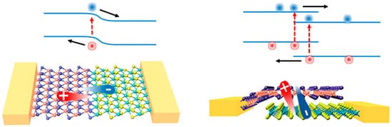
Figure 5. In-plane p–n junction (left) and out-of-plane p–n junction (right) of 2D materials, and their respective electronic band alignment. Reprinted with permission from ref. [6]. © 2017, AIP Publishing.
This entry is adapted from the peer-reviewed paper 10.3390/s21082758
This entry is offline, you can click here to edit this entry!