Your browser does not fully support modern features. Please upgrade for a smoother experience.
Please note this is an old version of this entry, which may differ significantly from the current revision.
Subjects:
Nanoscience & Nanotechnology
Low-temperature cooling possesses advantages in applicability, stability and nondamaging characteristics. Because of the temperature-related physical properties of nanoscale materials.
- temperature dependence
- photoelectric
1. Introduction
To meet the emergent requirement of the development of sustainable and clean energy, solar energy, recognized as the best potential alternative to fossil-fuel power, has been intensively investigated regarding its effective harvesting, conversion and storage in past decades [1][2][3][4][5][6][7][8][9]. One of the major developments lies in the mature utilization of nanoscale materials, such as two-dimensional materials [10][11] and quantum dots [12]. However, the advent of the photoelectric device also raises concerns regarding adaptivity to diversified environments, such as outer space or other extreme environments. Differing from the widely researched performance at normal temperature condition, the investigations on extreme temperature conditions, especially low temperature, are insufficient for completing the underlying physical mechanism and applying it to practical use. There are a handful of reports showing decreased performance at low temperature. These weakening phenomena caused by lowering temperature are ascribed to many causes including frozen carrier diffusion [13], reduced absorption [14], interfacial ion accumulation [15], phase transition [16] and radiative [17] and nonradiative [18] recombination. However, there are also many reports that low-temperature operation is not a restriction but an enhancement to overall photoelectric performance, ranging from low-dimension materials to nanocrystals. The effectiveness of the cooling method on these devices not only provides a strategy for constructing photoelectric devices under extreme conditions but also reveals the potential of cooling as an innovative and efficacious method for improving optoelectronic performance. It is worth noting that small drops in temperature will also cause visible improvement in photoelectric performance [19][20][21]. No matter the need, in applications or in theoretical research, relevant reports on the cooling method is in urgent need of systematic summary and guidance.
To realize improvements through low-temperature cooling, the underlying function mechanism deserves investigation. Similar to coupling effects or surface modification [22][23][24][25][26], the cooling method functions without changing composition or inherent structures. Moreover, compared with these traditional methods, cooling’s enhanced effects have unique advantages in applicability, stability and nondestructive characteristics. In view of the existing theories, the general temperature-dependent methods can be divided into three aspects: materials, devices and performances, shown in Figure 1. Temperature variation first directly functions on materials, inducing fluctuations in energy level [27][28][29], carrier motions [30], density of traps/carriers [31] and crystal structure transition [32]. For cooling-enhanced materials, regulation in energy levels causes changes in absorption [28], barrier height [33] and so on [34][35], then influences photon absorption and charge transportation. Some intrinsic characteristics of carriers are reported to show huge enhancement from cooling, including mobility [36], diffusion length [37] and corresponding densities [38]. For specific materials, structure transition [39] has been observed in a low-temperature range, providing more potential for cooling regulation. When the above phenomena integrated with devices, the cooling-enhanced properties in devices can be classified into absorption [40], carrier diffusion and recombination [41][42], resistance [43], photoconductivity [44], permittivity [45], interfaces and defects [46] and can improve the overall performance of both photodetectors and solar cells. The full mechanism is based on temperature-dependent optical and electrical properties, thus the emergence of the utilization of the cooling method, which possesses many advantages over conventional improvement methods and also possesses benefits to reliable photoelectric application in harsh environments.
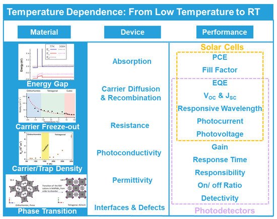
Figure 1. Temperature-dependent effect on photoelectric devices including materials, devices and performances. All images reproduced with permission: “Bandgap” (adapted from [29], with permission from the American Institute of Physics, 2014). “Carrier freeze-out” (adapted from [30], with permission from Wiley-VCH, 2015). “Carrier/Trap Density” (adapted from [31], with permission from Wiley-VCH, 2017). “Phase Transition” (adapted from [32], with permission from Wiley-VCH, 2018).
2. Applications of the Low-Temperature-Enhanced Photoelectric Process
Advances in cooling-enhanced photoelectronic processes bring new opportunities to conventional photoelectrical nanomaterials, based on superiority in tuneable band alignment, suppressed noise current, a different mechanism of charge motion and so on, hence, enabling more innovative optoelectronic applications. The cooling method has been widely used in the photodetection field, especially for background-limited infrared photodetectors. As shown in Figure 2(a1), summarised by Wang et al., typical high-resolution photodetectors in the infrared field are dominated by materials with low-temperature operating requirements [47]. In addition to reduced dark current at cryogenic temperatures, significant enhanced detectivity makes the cooling method a more effective strategy for realizing highly sensitive photodetection. As shown, for example, by Figure 2(a2,a3), the III-V group photodetector acquires accuracy to distinguish details such as vessels when the temperature further drops to 60 K [48]. Despite difficulties in operation at extremely low temperature, the negative relationship between the temperature and the photoresponse of the discussed materials provides feasibility in greatly increasing devices’ performance using the proper cooling process. In contrast to the mature application of cooling in photodetection, solar cells possessing complex configuration and integrated optoelectrical mechanisms are in the beginning stage. Recently, Chen et al. successfully fabricated an unencapsulated perovskite device exhibiting higher performance in a simulated near-space (especially low-temperature) environment [49]. The enhancement at low temperature mainly originates from the self-elimination of intrinsic defects brought by phase transition under a cooling environment. As illustrated in Figure 8b, when temperatures decrease from 300 K to 220 K, the phase transition from cubic to tetragonal structure eliminates these intrinsic point defects then causes PCE to increase to 25.2% at 220 K. Previous discussion also lists the utilization of the frozen hysteresis effect at suitable temperature to improve the conversion efficiency of perovskite solar cells. Further investigations are expected to demonstrate the enormous advantages of cooling-enhanced solar cells, especially perovskite in space, near polar regions and other cool conditions. Integrated optoelectronic effects with other sensing functions play an important role in next-generation communication, healthcare, bioelectronics and so on [23][50][51][52][53][54][55][56][57][58][59][60][61]. In 2020, Chang et al. investigated the low-temperature cooling-enhanced pryo-phototronic effect on SnS/CdS photodetectors, depicted in Figure 2(c1,c2). For this planar structure photodetector, significant enhancement (~500%) of the ratio of pyroelectric to total signal was achieved as temperature declined to 77 K [62]. Further research on ZnO/perovskite [63] and p-Si/n-ZnO [64] verified that low temperature improved the coupling effect phenomenon. The coupling mechanism was unveiled by Ma et al. with experiments on BaTiO3 [65], shown in Figure 2(c3,c4). Under low-temperature operation, shallow trap levels play a more important role in photoinduced response. At room temperature, the function of shallow traps has been suppressed. However, the temperature dependence of piezo-photoelectric effect showed that cooling weakens piezoelectric and photoelectric performance [66][67]; these results remain a puzzle in the investigation of photoelectricity-evolved coupling mechanisms at low temperature. More multifunctional detectors operating at low temperature deserve investigation, especially those based on low-temperature-enhancing mechanisms. Another challenge for cooling operations is the limit of difficulties in realizing extremely low temperatures. According to specific temperature-dependent effects of optoelectronic devices, it is recommended to lock in optimal performance by cooling to the proper temperature rather than extreme low temperature. For the negative temperature-dependent section, even slightly cooler temperature will cause invisible improvement. In this regard, we believe that investigations on cooling-enhanced performance will make breakthroughs in low-temperature photoelectric application and push forward research on temperature-regulated optoelectrical mechanisms.
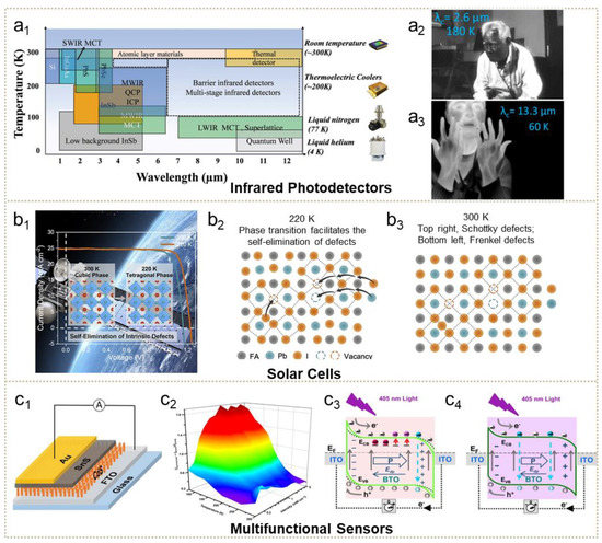
Figure 2. Applications of the low-temperature cooling method for photoelectric devices. (a) Cooling application in infrared photodetectors. (a1) Summary of working temperature for infrared photodetectors (adapted from [47], with permission from Wiley-VCH, 2019). (a2,a3) Temperature-dependent sensing performance of infrared photodetectors (adapted from [48], with permission from the Multidisciplinary Digital Publishing Institute, 2020). (b) Cooling application in solar cells (adapted from [49], with permission from Elsevier, 2020). (c) Cooling application in multifunction sensors. (c1,c2) Cooling-enhanced pyro-photoelectric coupling effect (adapted from [62], with permission from Wiley-VCH, 2020). (c3,c4) The underlying cooling-enhanced mechanism of the coupling effect (adapted from [65], with permission from Elsevier, 2019).
This entry is adapted from the peer-reviewed paper 10.3390/nano11051131
References
- Jung, H.S.; Park, N.G. Perovskite solar cells: From materials to devices. Small 2015, 11, 10–25.
- Tian, W.; Liu, D.; Cao, F.; Li, L. Hybrid Nanostructures for Photodetectors. Adv. Opt. Mater. 2016, 5, 4.
- Koppens, F.H.L.; Mueller, T.; Avouris, P.; Ferrari, A.C.; Vitiello, M.S.; Polini, M. Photodetectors based on graphene, other two-dimensional materials and hybrid systems. Nat. Nanotechnol. 2014, 9, 780–793.
- Nasiri, N.; Jin, D.; Tricoli, A. Nanoarchitechtonics of Visible-Blind Ultraviolet Photodetector Materials: Critical Features and Nano-Microfabrication. Adv. Opt. Mater. 2019, 7, 2.
- Guo, W.; Yang, Y.; Qi, J.; Zhao, J.; Zhang, Y. Localized ultraviolet photoresponse in single bent ZnO micro/nanowires. Appl. Phys. Lett. 2010, 97, 133112.
- Yang, Y.; Zhang, H.; Lin, Z.-H.; Liu, Y.; Chen, J.; Lin, Z.; Zhou, Y.S.; Wong, C.P.; Wang, Z.L. A hybrid energy cell for self-powered water splitting. Energy Environ. Sci. 2013, 6, 2429–2434.
- Ouyang, B.; Zhang, K.; Yang, Y. Self-Powered UV Photodetector Array Based on P3HT/ZnO Nanowire Array Hetero-junction. Adv. Mater. Technol. 2017, 2, 1700208.
- Ouyang, B.; Zhang, K.; Yang, Y. Photocurrent Polarity Controlled by Light Wavelength in Self-Powered ZnO Nanowires/SnS Photodetector System. iScience 2018, 1, 16–23.
- Qi, J.; Ma, N.; Ma, X.; Adelung, R.; Yang, Y. Enhanced Photocurrent in BiFeO3 Materials by Coupling Temperature and Thermo-Phototronic Effects for Self-Powered Ultraviolet Photodetector System. ACS Appl. Mater. Interfaces 2018, 10, 13712–13719.
- Glavin, N.R.; Rao, R.; Varshney, V.; Bianco, E.; Apte, A.; Roy, A.; Ringe, E.; Ajayan, P.M. Emerging Applications of Elemental 2D Materials. Adv. Mater. 2020, 32, e1904302.
- Lan, C.; Shi, Z.; Cao, R.; Li, C.; Zhang, H. 2D materials beyond graphene toward Si integrated infrared optoelectronic devices. Nanoscale 2020, 12, 11784–11807.
- Wu, J.; Lu, Y.; Feng, S.; Wu, Z.; Lin, S.; Hao, Z.; Yao, T.; Li, X.; Zhu, H.; Lin, S. The Interaction between Quantum Dots and Graphene: The Applications in Graphene-Based Solar Cells and Photodetectors. Adv. Funct. Mater. 2018, 28, 50.
- Cojocaru, L.; Uchida, S.; Sanehira, Y.; Gonzalez-Pedro, V.; Bisquert, J.; Nakazaki, J.; Kubo, T.; Segawa, H. Temperature Effects on the Photovoltaic Performance of Planar Structure Perovskite Solar Cells. Chem. Lett. 2015, 44, 1557–1559.
- Chang, C.; Li, H.; Huang, S.H.; Cheng, H.H.; Sun, G.; Soref, R.A. Sn-based Ge/Ge0.975Sn0.025/Ge p-i-n photodetector operated with back-side illumination. Appl. Phys. Lett. 2016, 108, 151101.
- Cao, R.; Xu, F.; Zhu, J.; Ge, S.; Wang, W.; Xu, H.; Xu, R.; Wu, Y.; Ma, Z.; Hong, F.; et al. Unveiling the Low-Temperature Pseudodegradation of Photovoltaic Performance in Planar Perovskite Solar Cell by Optoelectronic Observation. Adv. Energy Mater. 2016, 6, 18.
- Zhang, H.; Qiao, X.; Shen, Y.; Moehl, T.; Zakeeruddin, S.M.; Grätzel, M.; Wang, M. Photovoltaic behaviour of lead methylammonium triiodide perovskite solar cells down to 80 K. J. Mater. Chem. A 2015, 3, 11762–11767.
- Davies, C.L.; Filip, M.R.; Patel, J.B.; Crothers, T.W.; Verdi, C.; Wright, A.D.; Milot, R.L.; Giustino, F.; Johnston, M.B.; Herz, L.M. Bimolecular recombination in methylammonium lead triiodide perovskite is an inverse absorption process. Nat. Commun. 2018, 9, 1–9.
- Woo, H.C.; Choi, J.W.; Shin, J.; Chin, S.-H.; Ann, M.H.; Lee, C.-L. Temperature-Dependent Photoluminescence of CH3NH3PbBr3 Perovskite Quantum Dots and Bulk Counterparts. J. Phys. Chem. Lett. 2018, 9, 4066–4074.
- Weng, B.; Qiu, J.; Zhao, L.; Chang, C.; Shi, Z. CdS/PbSe heterojunction for high temperature mid-infrared photovoltaic detector applications. Appl. Phys. Lett. 2014, 104, 121111.
- Arora, H.; Dong, R.; Venanzi, T.; Zscharschuch, J.; Schneider, H.; Helm, M.; Feng, X.; Cánovas, E.; Erbe, A. Demonstration of a Broadband Photodetector Based on a Two-Dimensional Metal–Organic Framework. Adv. Mater. 2020, 32, e1907063.
- Wei, W.; Bao, X.-Y.; Soci, C.; Ding, Y.; Wang, Z.-L.; Wang, D. Direct Heteroepitaxy of Vertical InAs Nanowires on Si Substrates for Broad Band Photovoltaics and Photodetection. Nano Lett. 2009, 9, 2926–2934.
- Wang, Y.; Zhu, L.; Feng, Y.; Wang, Z.; Wang, Z.L. Comprehensive Pyro-Phototronic Effect Enhanced Ultraviolet Detector with ZnO/Ag Schottky Junction. Adv. Funct. Mater. 2018, 29.
- Ma, N.; Zhang, K.; Yang, Y. Photovoltaic–Pyroelectric Coupled Effect Induced Electricity for Self-Powered Photodetector System. Adv. Mater. 2017, 29, 46.
- Zhang, Y.; Zhai, J.; Wang, Z.L. Piezo-Phototronic Matrix via a Nanowire Array. Small 2017, 13, 1702377.
- Liu, Y.; Yang, Q.; Zhang, Y.; Yang, Z.; Wang, Z.L. Nanowire Piezo-phototronic Photodetector: Theory and Experimental Design. Adv. Mater. 2012, 24, 1410–1417.
- Datta, S.; Gokhale, M.R.; Shah, A.P.; Arora, B.M.; Kumar, S. Temperature dependence of surface photovoltage of bulk semiconductors and the effect of surface passivation. Appl. Phys. Lett. 2000, 77, 4383–4385.
- Soibel, A.; Keo, S.A.; Fisher, A.; Hill, C.J.; Luong, E.; Ting, D.Z.; Gunapala, S.D.; Lubyshev, D.; Qiu, Y.; Fastenau, J.M.; et al. High operating temperature nBn detector with monolithically integrated microlens. Appl. Phys. Lett. 2018, 112, 041105.
- Villegas, C.E.P.; Rocha, A.R.; Marini, A. Anomalous Temperature Dependence of the Band Gap in Black Phosphorus. Nano Lett. 2016, 16, 5095–5101.
- Soibel, A.; Hill, C.J.; Keo, S.A.; Höglund, L.; Rosenberg, R.; Kowalczyk, R.; Khoshakhlagh, A.; Fisher, A.; Ting, D.Z.-Y.; Gunapala, S.D. Room temperature performance of mid-wavelength infrared InAsSb nBn detectors. Appl. Phys. Lett. 2014, 105, 023512.
- Milot, R.L.; Eperon, G.E.; Snaith, H.J.; Johnston, M.B.; Herz, L.M. Temperature-Dependent Charge-Carrier Dynamics in CH3NH3PbI3 Perovskite Thin Films. Adv. Funct. Mater. 2015, 25, 6218–6227.
- Landi, G.; Neitzert, H.C.; Barone, C.; Mauro, C.; Lang, F.; Albrecht, S.; Rech, B.; Pagano, S. Correlation between Elec-tronic Defect States Distribution and Device Performance of Perovskite Solar Cells. Adv. Sci. 2017, 4, 1700183.
- Yang, B.; Ming, W.; Du, M.H.; Keum, J.K.; Puretzky, A.A.; Rouleau, C.M.; Huang, J.; Geohegan, D.B.; Wang, X.; Xiao, K. Real-Time Observation of Order-Disorder Transformation of Organic Cations Induced Phase Transition and Anomalous Photoluminescence in Hybrid Perovskites. Adv. Mater. 2018, 30, e1705801.
- Grotevent, M.J.; Hail, C.U.; Yakunin, S.; Bachmann, D.; Kara, G.; Dirin, D.N.; Calame, M.; Poulikakos, D.; Kovalenko, M.V.; Shorubalko, I. Temperature-Dependent Charge Carrier Transfer in Colloidal Quantum Dot/Graphene Infrared Photodetectors. ACS Appl. Mater. Interfaces 2020, 13, 848–856.
- Dar, M.I.; Jacopin, G.; Meloni, S.; Mattoni, A.; Arora, N.; Boziki, A.; Zakeeruddin, S.M.; Rothlisberger, U.; Grätzel, M. Origin of unusual bandgap shift and dual emission in organic-inorganic lead halide perovskites. Sci. Adv. 2016, 2, e1601156.
- Ravikumar, A.P.; Chen, G.; Zhao, K.; Tian, Y.; Prucnal, P.R.; Tamargo, M.C.; Gmachl, C.F.; Shen, A. Room Temperature and High Responsivity Short Wavelength II-VI Quantum Well Infrared Photodetector. Appl. Phys. Lett. 2013, 102, CTh4J.3.
- Milot, R.L.; Klug, M.T.; Davies, C.L.; Wang, Z.; Kraus, H.; Snaith, H.J.; Johnston, M.B.; Herz, L.M. The Effects of Doping Density and Temperature on the Optoelectronic Properties of Formamidinium Tin Triiodide Thin Films. Adv. Mater. 2018, 30, e1804506.
- McClintock, L.; Xiao, R.; Hou, Y.; Gibson, C.; Travaglini, H.C.; Abramovitch, D.; Tan, L.Z.; Senger, R.T.; Fu, Y.; Jin, S.; et al. Temperature and Gate Dependence of Carrier Diffusion in Single Crystal Methylammonium Lead Iodide Perovskite Microstructures. J. Phys. Chem. Lett. 2020, 11, 1000–1006.
- Piana, G.M.; Bailey, C.G.; Lagoudakis, P.G. Phonon-Assisted Trapping and Re-excitation of Free Carriers and Excitons in Lead Halide Perovskites. J. Phys. Chem. C 2019, 123, 19429–19436.
- Greenland, C.; Shnier, A.; Rajendran, S.K.; Smith, J.A.; Game, O.S.; Wamwangi, D.; Turnbull, G.A.; Samuel, I.D.W.; Billing, D.G.; Lidzey, D.G. Correlating Phase Behavior with Photophysical Properties in Mixed-Cation Mixed-Halide Perovskite Thin Films. Adv. Energy Mater. 2019, 10, 4.
- Liu, Y.; Lu, H.; Niu, J.; Zhang, H.; Lou, S.; Gao, C.; Zhan, Y.; Zhang, X.; Jin, Q.; Zheng, L. Temperature-dependent photoluminescence spectra and decay dynamics of MAPbBr3 and MAPbI3 thin films. AIP Adv. 2018, 8, 095108.
- Tan, M.; Chen, B.; Zhang, Y.; Ni, M.; Wang, W.; Zhang, H.; Zhou, Q.; Bao, Y.; Wang, Y. Temperature-Dependent Dynamic Carrier Process of FAPbI3 Nanocrystals’ Film. J. Phys. Chem. C 2020, 124, 5093–5098.
- Gélvez-Rueda, M.C.; Renaud, N.; Grozema, F.C. Temperature Dependent Charge Carrier Dynamics in Formamidinium Lead Iodide Perovskite. J. Phys. Chem. C 2017, 121, 23392–23397.
- Hu, L.; Wu, L.; Liao, M.; Hu, X.; Fang, X. Electrical Transport Properties of Large, Individual NiCo2O4 Nanoplates. Adv. Funct. Mater. 2012, 22, 998–1004.
- Li, L.; Fang, X.; Zhai, T.; Liao, M.; Gautam, U.K.; Wu, X.; Koide, Y.; Bando, Y.; Golberg, D. Electrical Transport and High-Performance Photoconductivity in Individual ZrS2 Nanobelts. Adv. Mater. 2010, 22, 4151–4156.
- Fabini, D.H.; Stoumpos, C.C.; Laurita, G.; Kaltzoglou, A.; Kontos, A.G.; Falaras, P.; Kanatzidis, M.G.; Seshadri, R. Reentrant Structural and Optical Properties and Large Positive Thermal Expansion in Perovskite Formamidinium Lead Iodide. Angew. Chem. Int. Ed. Engl. 2016, 55, 15392–15396.
- Zhang, X.; Bi, S.; Zhou, J.; You, S.; Zhou, H.; Zhang, Y.; Tang, Z. Temperature-dependent charge transport in solu-tion-processed perovskite solar cells with tunable trap concentration and charge recombination. J. Mater. Chem. C 2017, 5, 9376–9382.
- Wang, P.; Xia, H.; Li, Q.; Wang, F.; Zhang, L.; Li, T.; Martyniuk, P.; Rogalski, A.; Hu, W. Sensing Infrared Photons at Room Temperature: From Bulk Materials to Atomic Layers. Small 2019, 15, e1904396.
- Ting, D.Z.; Rafol, S.B.; Khoshakhlagh, A.; Soibel, A.; Keo, S.A.; Fisher, A.M.; Pepper, B.J.; Hill, C.J.; Gunapala, S.D. InAs/InAsSb Type-II Strained-Layer Superlattice Infrared Photodetectors. Micromachines 2020, 11, 958.
- Chen, Y.; Tan, S.; Li, N.; Huang, B.; Niu, X.; Li, L.; Sun, M.; Zhang, Y.; Zhang, X.; Zhu, C.; et al. Self-Elimination of Intrinsic Defects Improves the Low-Temperature Per-formance of Perovskite Photovoltaics. Joule 2020, 4, 1961–1976.
- Yang, Y.; Wang, Z.L. Hybrid energy cells for simultaneously harvesting multi-types of energies. Nano Energy 2015, 14, 245–256.
- Zhang, K.; Wang, Z.L.; Yang, Y. Enhanced P3HT/ZnO Nanowire Array Solar Cells by Pyro-phototronic Effect. ACS Nano 2016, 10, 10331–10338.
- Ma, N.; Yang, Y. Boosted photocurrent in ferroelectric BaTiO3 materials via two dimensional planar-structured contact configurations. Nano Energy 2018, 50, 417–424.
- Zhang, K.; Wang, S.; Yang, Y. A One-Structure-Based Piezo-Tribo-Pyro-Photoelectric Effects Coupled Nanogenerator for Simultaneously Scavenging Mechanical, Thermal, and Solar Energies. Adv. Energy Mater. 2016, 7, 1601852.
- Ji, Y.; Zhang, K.; Yang, Y. A One-Structure-Based Multieffects Coupled Nanogenerator for Simultaneously Scavenging Thermal, Solar, and Mechanical Energies. Adv. Sci. 2018, 5, 1700622.
- Qi, J.; Ma, N.; Yang, Y. Photovoltaic-Pyroelectric Coupled Effect Based Nanogenerators for Self-Powered Photodetector System. Adv. Mater. Interfaces 2018, 5, 3.
- Zhang, K.; Yang, Y. Thermo-Phototronic Effect Enhanced InP/ZnO Nanorod Heterojunction Solar Cells for Self-Powered Wearable Electronics. Adv. Funct. Mater. 2017, 27, 1703331.
- Song, K.; Ma, N.; Mishra, Y.K.; Adelung, R.; Yang, Y. Achieving Light-Induced Ultrahigh Pyroelectric Charge Density Toward Self-Powered UV Light Detection. Adv. Electron. Mater. 2019, 5, 1.
- Zhao, R.; Ma, N.; Qi, J.; Mishra, Y.K.; Adelung, R.; Yang, Y. Optically Controlled Abnormal Photovoltaic Current Mod-ulation with Temperature in BiFeO3. Adv. Electron. Mater. 2019, 5, 1800791.
- Zhang, R.; Hummelgård, M.; Örtegren, J.; Olsen, M.; Andersson, H.; Yang, Y.; Olin, H. Human Body Constituted Tri-boelectric Nanogenerators as Energy Harvesters, Code Transmitters, and Motion Sensors. ACS Appl. Energ. Mater. 2018, 1, 2955–2960.
- Zhao, K.; Ouyang, B.; Bowen, C.R.; Wang, Z.L.; Yang, Y. One-structure-based multi-effects coupled nanogenerators for flexible and self-powered multi-functional coupled sensor systems. Nano Energy 2020, 71, 104632.
- Ji, Y.; Wang, Y.; Yang, Y. Photovoltaic–Pyroelectric–Piezoelectric Coupled Effect Induced Electricity for Self-Powered Coupled Sensing. Adv. Electron. Mater. 2019, 5, 1900195.
- Chang, Y.; Wang, J.; Wu, F.; Tian, W.; Zhai, W. Structural Design and Pyroelectric Property of SnS/CdS Heterojunctions Contrived for Low-Temperature Visible Photodetectors. Adv. Funct. Mater. 2020, 30, 23.
- Peng, W.; Yu, R.; Wang, X.; Wang, Z.; Zou, H.; He, Y.; Wang, Z.L. Temperature dependence of pyro-phototronic effect on self-powered ZnO/perovskite heterostructured photodetectors. Nano Res. 2016, 9, 3695–3704.
- Dong, J.; Wang, Z.; Wang, X.; Wang, Z.L. Temperature dependence of the pyro-phototronic effect in self-powered p-Si/n-ZnO nanowires heterojuncted ultraviolet sensors. Nano Today 2019, 29, 100798.
- Ma, N.; Yang, Y. Boosted photocurrent via cooling ferroelectric BaTiO3 materials for self-powered 405 nm light detection. Nano Energy 2019, 60, 95–102.
- Yu, R.; Wang, X.; Wu, W.; Pan, C.; Bando, Y.; Fukata, N.; Hu, Y.; Peng, W.; Ding, Y.; Wang, Z.L. Temperature Dependence of the Piezophototronic Effect in CdS Nanowires. Adv. Funct. Mater. 2015, 25, 5277–5284.
- Wang, X.; Yu, R.; Peng, W.; Wu, W.; Li, S.; Wang, Z.L. Temperature Dependence of the Piezotronic and Piezophototronic Effects ina-axis GaN Nanobelts. Adv. Mater. 2015, 27, 8067–8074.
This entry is offline, you can click here to edit this entry!