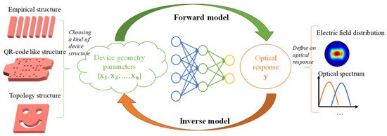
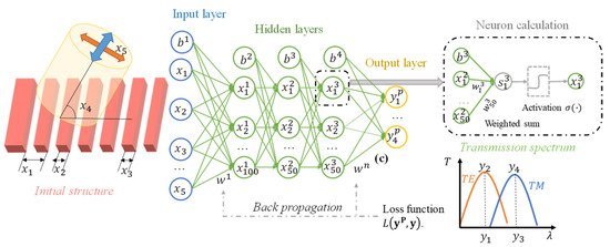
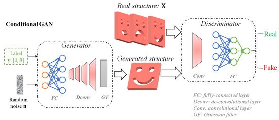
2.2. Optimization of Empirical Structures
An empirical structure makes use of classical structures, where only a few parameters like radius, duty cycle, widths of waveguides, etc. are tuned for targeted optical response. These classical structures are proposed by researchers for different application scenarios. For example, micro-rings are preferred for wavelength selection due to their high wavelength-sensitivity [
21,
27]. Directional couplers (DCs) are used for polarization beam splitters (PBS), mode-division multiplexers (MDM) and wavelength-division multiplexers (WDM) since DCs couple light from one waveguide to another in a reciprocating way [
21,
24,
26]. Y-splitter with three ports is widely used for power splitting (PS) [
59]. Mach-Zehnder interferometer (MZI) can separate light and finally combine with optical path difference, so that it could be utilized for optical switches or modulators [
30,
60,
61]. Gratings which periodically arrange the silicon and air (or silica) have been applied to manipulate the effective refractive index of waveguides or act as fiber grating couplers (GC) [
62,
63]. With known structures and underlying theories to design a device for targeted FOM, it still costs lots of time to tailor the key parameters, as each parameter set requires at least one EM simulation.
The relationship between the abstracted key parameters from an empirical structure and its optical response is a kind of NP hard problem, which can be solved by heuristic algorithms. GA, a kind of heuristic optimized algorithm, is inspired by Darwinian evolution theory of survival of the fittest [
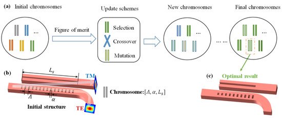
64]. After initial chromosomes, which represent different parameter sets, are randomly generated, the fitness values describing the FOM of each chromosome are computed as shown in a. Chromosome with better fitness values will be chosen as elite and passed to the next generation directly. For the rest of chromosomes, some chromosomes experience crossover with others to create new chromosomes and some produce offspring by mutation. Through the above elite selection, crossover and mutation, a new generation is born. This procedure is repeated until the best FOM is found.
Figure 2. Schematic diagram of GA for the design of PBS based on directional coupler. (a) Operating principle of GA. (b) Initial structure of PBS and abstracted parameters. (c) Final structure of optimized PBS.
We take reference [
25] for example to illustrate utilizing GA to optimize an optical device with empirical structure. A broadband PBS based on directional coupler and subwavelength gratings (SWGs) structure is designed as shown in b. Key parameters like pitch , duty cycle and coupling length are abstracted to represent this structure and coded as a chromosome. Initial chromosomes (20 parameters sets) are generated randomly within parameter boundaries. The FOM of each chromosome is calculated with respect to the output of transverse electric (TE) mode at through waveguide and transverse magnetic (TM) mode at cross waveguide. After hundreds of iterations, the best parameter set is found as c suggests, where the transmission efficiencies for both TE and TM modes at desired output ports are larger than 85% over wavelength range from 1250 nm to 1680 nm.
Another popular heuristic algorithm is PSO [
65]. Different form GA, where parts of parameter sets are updated at each iteration, PSO updates all the parameter sets towards the global optimized FOM. For PSO, the initial randomly generated parameter sets are called particles, each of which is assigned an initial velocity. PSO evaluates the FOM of each particle and finds the best global and local FOMs as well as the corresponding particles. According to the global best particle and the local best particle at their current iteration, the velocity of each particle is updated. With updated velocities, the new population are generated from original particles. This updating procedure is repeated until the global best FOM is converged to an acceptable value. PSO has also been widely used for the design of silicon photonic devices with empirical structures as listed in .
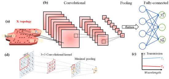
2.3. Optimization of QR-Code like Structures
A QR-code like structure, where regular shapes like circles or rectangles are selectively etched on a periodic 2-D surface, is also an important approach for manipulating light propagation in waveguides. Different from empirical structure-based design, QR-code like structure with hundreds of DOF is a more general approach for different problems. In a QR-code like structure, designers only have to define the pitch and size of etched holes as well as the footprint of design area. For each hole, to be etched or not is determined automatically to achieve better FOM. Using a compact QR-code like structure, many different functional components like power splitter [
41,
45], polarization rotator [
33,
42,
44], PBS [
40], WDM [
42], MDM [
34,
39], crossing [
66], GC [
67] and photonic crystal [
68] have been designed.
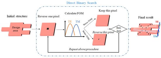
DBS, a brute-force searching algorithm, initially proposed by Seldowitz et al. for the synthesis of digital holograms [
69], has been proven to be efficient for the design of devices with QR-code structure. Shen et al. introduced DBS to design a very compact integrated PBS on SOI platform [
40], as shown in . They defined the size of design area to be 2.4 × 2.4 μm
2 with each hole size to be 0.12 × 0.12 μm
2. There are 400 rectangular pixels to determine whether to etch or not. During each iteration, one pixel in the design area is reversed and the FOM (average transmission efficiency of TE and TM modes at the targeted output ports) is calculated and compared with the FOM for last iteration. If the new FOM is larger than the old one, the new geometry with reversed pixel is past to the next generation, otherwise, the old geometry is kept. The above procedure is repeated until the FOM is large enough to be acceptable. After about 140 h of optimization, the average transmission efficiency of optimized PBS is higher than 70% and its 1 dB bandwidth is 83 nm.
Figure 3. Schematic of DBS-assisted PBS design based on QR-code like structure.
In addition to DBS, heuristic algorithms like GA and PSO have also been applied for the design of integrated silicon photonic devices based on QR-code like structure. Different from DBS, which updates one pixel at each iteration, heuristic algorithms code all the pixels as an individual and update them together during each iteration, hence the total number of iterations could be reduced.
2.4. Optimization of Irregular Structures
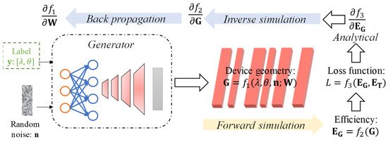
An irregular structure owns the highest DOF since the whole design area is segmented into very small pixels [
15]. Different from QR-code like structure which also pixelates the design area with 100 or 200 nm resolution, an irregular structure is more intricate with ultra-high resolution (10 or 20 nm scale). It would be extremely time-consuming for gradient-free algorithms discussed above to optimize an irregular structure with thousands of DOF, as the required simulations is proportional to the number of DOF. Fortunately, gradient-based algorithms cast light on this time-consuming problem, where all the parameters are updated with the fewest simulations.
To describe the optimization process, a mathematical model which tries to optimize the FOM at the constraints of Maxwell equations is built as in Equation (1):
where FOM
is the function of electric field
and magnetic field
. Permittivity
and permeability
in the design area are variables to be tuned for better FOM. Objective-first (OF) method [
56] and topology optimization (TO) with adjoint method [
70] have been proposed to solve Equation (1).
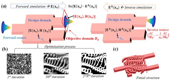
We take irregular PBS in reference [
71] as an example to illustrate the TO process. As shown in a, the design domain
is optimized by adjoint method for two FOMs. The first FOM is the transmission of TE mode at the upper arm while the second FOM is the transmission of TM mode at the lower arm.
Figure 4. Topology optimization of a PBS via adjoint method. (a) Schematic diagram of adjoint method. (b) Optimization process for the design area of PBS. (c) Final structure of optimized PBS.
As the optimization processes of two arms are similar, we only give detailed derivation of TE mode here. In the objective domain
, the actual EM fields are optimized towards fundamental TE mode. The targets at each position
in the objective domain is defined in the form of Poynting vectors [
70] as in Equation (2):
where
are the actual EM fields from the simulation, and
are the constant conjugated EM fields of the fundamental TE mode. The best target
requires the value of actual EM fields to be the largest and the direction of actual EM fields to be the same with fundamental TE mode at position
. However, it is still hard to determine whether the FOM is good or not when some positions get better targets while others get worse. Therefore, the total FOM is defined as the integral of all the targets in the objective domain as in Equation (3):
The derivative of total FOM to permittivity and permeability in the design domain
is calculated using chain rule. Firstly, the derivative of total FOM to actual EM fields in the objective domain
is calculated as in Equation (4):
where factors
are the constant values and are easy to get from Equation (2) as in Equation (5):
However, the terms
cannot be calculated analytically, as the relationship between
at objective domain and
at design domain cannot be expressed by an explicit function. Since the variation of permeability
causes little change to EM fields, only the variation of permittivity
is considered. In the design domain, the original geometry has electric field
at
. When a very small volume
at this position has a small permittivity change
, this will cause an induced dipole moment
Numerically, EM field variation
at
in the objective domain come from the summation effects of this induced dipole moments in the design domain, which can be expressed with Green’s function [
72] as in Equation (6):
where
and
represent the EM fields at
in the objective domain from a unit dipole at
in the design domain. The symmetry theory suggests the following relation as in Equation (7):
By substituting Equations (6) and (7) into Equation (4) and making an equivalent transformation, we get the total FOM as in Equation (8):
The inner integration is defined as the “adjoint” electric field
at position
in design domain as in Equation (9):
This adjoint electric field
can be obtained through the integration of all induced electric fields which come from EM dipoles with amplitudes
at different positions
at the objective domain. These amplitudes are constant values which are calculated by using Equation (5). Through an “inverse” simulation, where light source with amplitude
is placed in objective domain, all the adjoint fields in design domain can be numerically calculated. Substituting Equation (9) into Equation (8), the derivative of total FOM in the objective domain to permittivity
in the design domain is shown in Equation (10):
With one forward simulation which calculates all the electric fields
and one inverse simulation which computes all the adjoint electric fields
in the design domain, the derivatives of total FOM to all the permittivity
can be obtained as Equation (10) suggested. As discussed before, there are two FOMs for PBS. For another FOM’ which tries to guide TM mode to the second waveguide arm, the derivative of FOM’ to permittivity
in the design domain is also calculated in similar way. The permittivity in the design domain is updated towards the direction of total gradient decent as in Equation (11):
where
is the updating rate. The updating process is repeated until the gradient is small enough.
During the updating process, permittivity
is taken as a continuous variable for convenience of derivative calculation, which has to be discretized for real application scenarios. Both level-set [
73] and density optimization [
74] have been applied for discretization. In silicon platform, the design domain usually composes of silicon and silica (or air) with permittivity
and
, respectively. The level-set method defines a continuous variable
with values ranging from negative to positive.
suggests the boundary between two materials and the discrete permittivity in the design domain is defined as in Equation (12):
On the other hand, for density method, the values of continuous variable
range from 0 to 1, and the permittivity in the design domain is expressed as in Equation (13):
Different from level-set method which is discretized after applying Equation (12), the density method would generate “gray structures” with continuous permittivity between
and
. To further discretize permittivity, Su et al. proposed a discretization method by introducing self-biasing or neighbor-biasing [
46]. In the example of PBS design, density method is adopted and the optimization process is shown in b, where an initial random structure is finally optimized and discretized after 278 iterations.
Apart from discretization of permittivity, minimal feature size control is also an important issue for irregular structures as the large DOF bring features with critical size too small to be fabricated. Different approaches are proposed to solve this issue, such as density filters [
75], penalty functions [
76], artificial damping [
50] and morphological filters [
77]. Recently, Khoram et al. introduced b-splines to control minimal feature size of irregular structures [
78]. Instead of filtering out small features directly, this method transfers the design domain to lower space dimension composed of b-spline functions, which damps small features internally. In the example of PBS design, the optimized device geometry is shown in c, where density adjoint method with b-spline function is adopted. Within the footprint of 2.4 × 2.8 μm
2, this optimized PBS splits TE and TM modes with over 90% transmission efficiency covering 420-nm wavelength range.
2.5. Comparison of Iterative Optimization Algorithms for Silicon Photonics Design
We have discussed three examples of inverse designed PBSs via different initial structures with corresponding iterative optimization algorithms in the above three subsections. The PBS based on empirical structure has high transmission efficiency (over 85% within 420 nm wavelength range) for both TE and TM modes and the critical size is under the control of designers. However, it also has the largest footprint (approximately 7 × 4 μm2) and the lowest DOF (only 3). It takes about one week to optimize this device on two 12-core central processing units (CPUs). Profound prior knowledge about the coupling theory is also required and a skillful initial structure has to be chosen, otherwise, the device may not work at all. The PBS based on QR-code like structure has ultra-compact size (2.4 × 2.4 μm2) as well as high DOF (i.e., 400). Its design process does not need much prior knowledge but the optimization time is long (~140 design hours) as each QR-code has to be verified during DBS. This time-consuming optimization process limits both the size of footprint and the number of DOF, so the transmission efficiency of DBS optimized PBS is not very high. The peak efficiency of optimized PBS is ~80% and its 1 dB bandwidth is 83 nm. The irregular PBS optimized via adjoint method is also ultra-compact (2.8 × 2.4 μm2), and it has 16,800 DOF due to its ultra-high resolutions (i.e., 20 nm). After 64 h of optimization on two 12-core CPUs, the final irregular PBS has transmission efficiency over 90% covering 420-nm wavelength range. The irregular PBS has a time-efficient optimization process, where all the parameters can be updated in one round via only two simulations (one forward simulation and one adjoint simulation). However, profound knowledge about light-material interaction process, as well as advanced mathematics, is required for gradient calculations. Furthermore, gradient-based algorithms are easy to fall into local optimal. For example, the resolution of an irregular structure is usually 20 nm, which may result in minimal features too small to be fabricated.
Apart from the examples of PBS discussed above, inverse design based on these methods has been widely used for other silicon photonic devices as shown in . Empirical structure-based devices are large but they have high performance and are easy to process since their critical sizes are easy to control. QR-code like structures have compact footprints and controllable minimal feature sizes at the cost of some decrease in optical performance. Irregular devices have the most appealing performance, but minimal feature size control is in great need for the convenience of device fabrication.
Table 1. Examples of silicon photonic devices designed using iterative optimization algorithms.
Some researchers also combined different structures and algorithms to solve the limitations of certain methods for the design of a single device. For example, Xu et al. combined QR-code like structure into an empirical waveguide crossing structure to work as a wavelength filter [
35]. Xie et al. proposed a global optimization method combining GA and annealing algorithm for optimizing on-chip twisted light emitter [
81].