Your browser does not fully support modern features. Please upgrade for a smoother experience.
Please note this is an old version of this entry, which may differ significantly from the current revision.
Subjects:
Others
Electrically tunable phase gratings are able to steer an incoming light beam without employing movable parts. Here, we present the design and implementation of a 2D beam steering device by cascading two orthogonal 1D liquid crystal (LC) based phase gratings, each having an array of 72 rectangular individually controlled pixels and driven by a custom 12-bit Pulse-Width Modulation (PWM) electrical driver.
- Electrically Tunable Phase Gratings
1. Introduction
Pointing a laser beam accurately is relevant for many applications, such as optical tweezers [1], free space optical communications [2], and light detection and ranging [3,4,5]. To achieve this control, beam steering (BS) systems have been developed, both mechanical and non-mechanical [6].
There is a plethora of mechanical methods where movable micro-mirrors or micro-lenses steer a light beam by using piezo-actuators, rotating prisms, or microelectromechanical systems [7,8,9]. The main disadvantage of all these mechanical systems is that they need continuous adjustments to maintain alignment, and they can suffer from external noise [10]. Additionally, micromechanical systems with movable parts are scarcely acceptable for space applications because the harsh conditions during take-off and orbital steps easily jeopardize their stability and proper functioning.
Non-mechanical methods are widely used nowadays, such as acousto-optic and electro-optic deflectors [11,12] and liquid crystal spatial (LC) light modulators [13,14]. When compared to mechanical devices, non-mechanical devices offer a higher reliability, which makes them suitable for space applications [15]. For these devices, large steerable angles and large apertures are desirable.
LCs have been demonstrated to be a good candidate to implement non-mechanical beam steering devices due to their optical properties and swift response to moderate external electric fields. Optical Phased Arrays [16], Pancharatnam-Berry [17], Liquid Crystal on Silicon (LCoS) systems [18,19], and Polarization Gratings [20,21,22] are some solutions provided by LCs. LC devices are interesting when easy electronic driving, small size, light weight, non-mechanical parts, low power consumption, and low cost are considered as relevant requirements of the intended device.
LC beam steerers are usually prepared as phase-only devices. They are optical systems that interact with light, only modifying their phase and leaving other characteristics, such as wavelength or intensity, unchanged [23,24]. The aim of this work is to present a high fill factor LC BS device, capable of redirecting an impinging light beam in two dimensions (Figure 1). The steering angle is electronically tunable by spatially varying the retardation pattern of the liquid crystal.
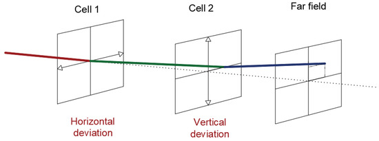
Figure 1. The combination of two 1D LC cells generating a 2D deviation in the incident angle.
2. Materials and Methods
2.1. Beam Steerers for Space Applications
Several LC structures can be used as beam steerers. Those intended to be applied to space environments need to account for resilience under ionizing radiation conditions. This usually excludes any LC device in which the active area includes electronics, such as the LCoS or the ubiquitous active-matrix thin-film transistor (AM-TFT). In both cases, LCoS and AM-TFT, electronics cannot be adequately shielded from ionizing radiation because the beam steerer must have visibility to outer space.
Passive-driven transmissive systems present a good alternative. The reliability of LC materials under ionizing radiation has already been tested [2]. In passive addressing mode, driving electronics are outside the steering cell, allowing the drivers to be adequately shielded.
The operation principle of this passive-addressed BS is based on phase diffraction gratings. Diffraction gratings are made of a set of linear parallel elements with a pitch comparable to the light wavelength [25]. Diffractive gratings are manufactured using different methods, as recently reviewed in [26].
The device presented in this work is driven digitally (Figure 2). Analog tunable beam steerers can be achieved using high resistivity electrodes [27], albeit with a limited scanning range. The transmissive device is a blaze-grating, i.e., a saw-tooth refractive index profile where every tooth is discretized in a number of steps by setting the effective refractive index of the liquid crystal, pixel by pixel [28,29]. Thus, as the light passes through the diffractive structure, it is deviated by an angle.
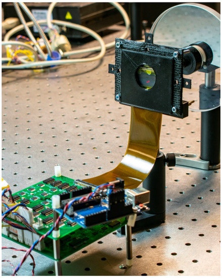
Figure 2. LC beam steering device. The LC cells are in their holder, with the electronic driver. The variable attenuator employed in the setup is also visible.
The diffraction efficiency is the relationship between the diffracted power and the input power. The larger the number of pixels per tooth, the better approximation to the continuous wedge profile, and the higher the diffraction efficiency, at a cost of reduced deviation angle. Fringing fields and crosstalk have been reported to cause a significant loss in efficiency [30,31].
2.2. Device Characteristics
The active area is defined by the pixel width and the total number of individual pixels. The employed nematic LC requires that the incoming light must be polarized. The birefringence of the LC delay the light polarized along the switching plane. The delay, δ(V)
is the effective birefrigence of the LC at a voltage, V.
The intensity variation follows the relationship in Equation (2):
In the diffractive phase graing, the continously varying phase is “wrapped” between 0π and 2π [32] (Figure 3). When the pattern corresponds to an integer number of pixels, a recurrent phase delay structure is observed along the grating. In this paper, the term “topology” is used to describe the total retardation of an equivalent wedge prism in which the maxima is t ⋅
2π; t being the topology number. The developed driver, which allows for individual addresing in the LC cell, means that the topology can be any fractional number. As an arbitrary convention, the positive sign of the topology has been asigned to deviation to the right and up along the two axes, respectively; Figure 4.
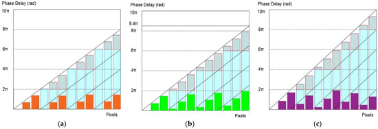
Figure 3. Schematic of the blaze grating structure over 12 pixels. The full colored orange, green, and purple rectangles present the wrapped phase delay of each pixel, corresponding to different integer and fractional topologies: (a) Topology +4, (b) Topology +4.2, (c) Topology +5. In all pictures, the sign of the topology is positive, corresponding to a deviation to the right or up.
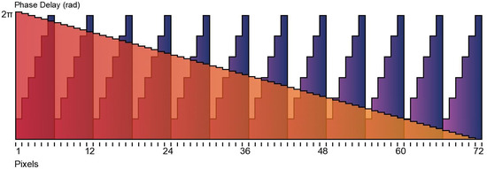
Figure 4. Schematic of the blaze grating for 72 pixels. The purple phase step structure corresponds with a topology +12 and the orange structure corresponds with a topology −1.
The deviation angle, θ
, generated by the blaze is a function of its period and working wavelength [33]:
Hence, the longer the wavelength or the shorter the period, the larger the diffraction angle, as long as the period is significantly larger than the wavelength. Additionally, the smaller the period, the smaller the pixels, in order not to compromise the diffraction efficiency, which is the real practical limiting factor in passive ITO based devices such as this one.
2.3. Manufacturing of LC Cells
The 1D liquid crystal cell is made up of an ITO coated glass sandwich that is filled up with nematic liquid crystal. One of the substrates is pixelated using a DLW technique, which allows generating high resolution structures in wafers with transparent ITO (Figure 5). The electrodes (pixels) are separated by less than 3 µm, leading to devices with a high fill factor [25]. The DLW installation (Lasing S.A.), consists of a UV laser with a CNC controlled XYZ-stage that shifts the substrate in XY while maintaining the focal distance using a second laser feedback system.
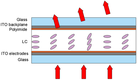
Figure 5. LC cell schematic, with their layer structure.
Both the pixelated and the continuous glass wafers were conditioned with rubbed polyimide PIA-2304(Chisso LIXON aligner, Tokyo, Japan), ensuring a uniform homogenous LC alignment. The cell thickness was controlled using randomly positioned 6.4 µm diameter cylindrical silica spacers. Once the cell is mounted and sealed, it is filled in vacuum with the positive nematic high birefringence liquid crystal MDA-98-1600 (Merck KGaA, Darmstadt, Germany). The thickness of the cell and the birefringence determined at 632 nm of the LC allow for an optical retardation variation of Δn632nm⋅L=0.266⋅6.4 μm=1.7 μm
, which means that, assuming that the reduction in birefringence does not exceed 10%, the manufactured cell will be applicable to wavelengths close to 1550 nm, which in turn would allow for twice the steering angle. The light transmission of the substrates limits the minimum working wavelength to about 400 nm.
Interconnections between the employed flex connector and the ITO electrodes were done using an Anisotropic Conductive Adhesive (Hitachi Chemical, Tokyo, Japan). In the contact area, the ITO between electrodes was eliminated by multiple ablation lines.
The free end of the flex connector was connected directly to the driving electronics, providing full and independent control of each of the electrodes.
2.4. The 2D Device
The 2D LC BS device is made up by cascading two orthogonal 1D liquid crystal cells. One is in charge of deviating the incident light beam in the azimuthal angle, while the other produces the deviation in the zenithal angle.
Both cells were manufactured following the same steps, and both were based on the same working principle of the LC. Each grating is made of 72 parallel pixels, with a 15 µm pitch. Interpixel size is kept smaller than 3 µm, reducing any fringe effect. The resulting active area is 1.1 × 1.1 mm2.
A CAD application was used to develop and design the pixel layout, including the active area and the fan-out (Figure 6). In the final cascaded configuration, the pixels of the two cells are perpendicular to each other in the active area. The rubbing direction, however, is common to both of the cells (Figure 7).
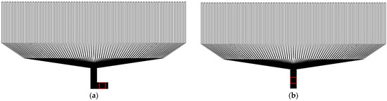
Figure 6. Pixel layout of the cells showing the contact fan-out. The active areas are marked with red squares. When overlapped, they create the 2D steering: (a) Horizontal pixels; (b) Vertical pixels.
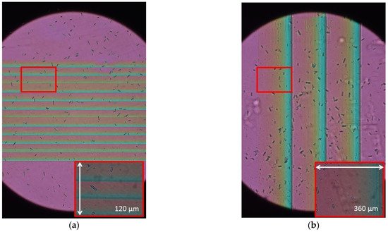
Figure 7. View of the active area in the microscope between cross polarizers: (a) Horizontal active area with topology +12 (pattern repetition for every 6 pixels, 90 µm); (b) Vertical active area with topology +3 (pattern repetition for every 24 pixels, 360 µm). Inserts show areas of 360 × 120 µm2, in which one may appreciate the individual pixels.
The incident light must be polarized in the same plane as the rubbing direction, determined in the manufacturing process.
2.5. Electronic Driver
An electronic driver has been specially designed for individual electronic control of every pixel of the LC cell (Figure 8). It employs a 12 bits PWM signal for each of the pixels of the two LC cells. The electronic driver is addressed using a standard SPI protocol. An Arduino UNO board acts as a USB-SPI for the communication between the controlling computer and the LC cell driver.
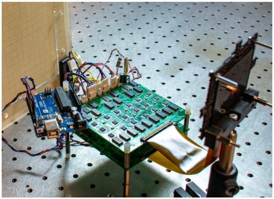
Figure 8. The 12 bits PWM driver that controls the LC cells.
The driver uses the 24 channel TLC5947 driver (PWM LED driver) from Texas Instrument (Dallas, TX, USA), with the output adjusted to TTL voltage levels by setting the control resistance to 18 kΩ and employing a 10 kΩ pull-up resistor. Each PWM voltage output is connected to the digital input of an analogue switch, ADG5413, from Analog Devices, which switches between an externally supplied AC signal and ground. The PWM cycle of approximately 1.3 µs is sufficiently fast for the LC to perceive only the effective RMS signal of the supplied AC field, which is a 5Vpp 1 kHz signal.
The TLC5947 may be daisy chained. In the presented driver, three TLCs are combined per driver board, and two boards are daisy chained, providing individual control of all the 144 (72 + 72) pixels in the two LC devices. The power consumption of the driver is less than 2 W.
2.6. Calibration
The LC cells were calibrated at room temperature (25°) to establish their relationship between driving PWM signal and induced phase delay, as previously described [34] (Figure 9).
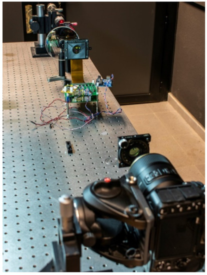
Figure 9. Calibration set up, including 632.8 nm He-Ne laser, attenuator, LC cells, electronic driver, polarizers, and camera.
The phase delay as a function of the PWM duty cycle (dc) follows a pseudo exponential decreasing function:
The fitted intensity curve (Equation (2)) was employed to calculate the required PWM for any desired retardation level used in the different topologies (Figure 10).
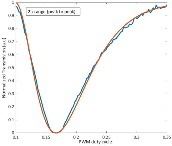
Figure 10. Normalized transmission intensity measured (blue) from the calibration, versus the fitted intensity (orange) as a function of the PWM duty cycle applied.
This entry is adapted from the peer-reviewed paper 10.3390/app11083632
This entry is offline, you can click here to edit this entry!