Nanomaterials science is becoming the foundation stone of high-frequency applications. The downscaling of electronic devices and components allows shrinking chip’s dimensions at a more-than-Moore rate. Many theoretical limits and manufacturing constraints are yet to be taken into account. A promising path towards nanoelectronics is represented by atomic-scale materials. In this entry, we offer a perspective on a specific class of devices, namely switches designed and fabricated using two-dimensional or nanoscale materials, like graphene, molybdenum disulphide, hexagonal boron nitride and ultra-thin oxides for high-frequency applications.
- microwaves
- atomic-scale devices
- 2D materials devices
- memristor
1. Introduction
The switch is a key device with multiple applications in nanoelectronics. A switch has two distinct states, i.e., ON and OFF, and these two states can be implemented in various ways. The electronic switch is a semiconductor component in which the carrier conduction is enabled (ON-state) or disabled (OFF-state) via a control parameter; the latter is the applied voltage in the case of two-terminal devices (such as diodes), or a gate voltage in the case of three-terminal devices. The digital electronics is based on these simple principles and a microprocessor contains billions of transistors integrated on a single chip, these transistors representing electronic switches dedicated to compute and memorize a huge quantity of information in a very short time. These digital switches have nano-sized dimensions, the ultimate target being their implementation with atomically thin materials, thus opening the path to electronics at atomic scale [1].
In the case of high-frequency signals, microwave or millimeter-wave switches are routing the signals between different ports, and hundreds or even thousands of them are used in a phased antenna array, in a transmission/reception system (e.g., radars) and in many high-quality items of equipment. In the ON-state, the high-frequency signals are transmitted between two different points of the same circuit, with a small insertion loss (i.e., less than 2 dB). By contrast, the OFF-state isolates two parts of a circuit and, in this case, the transmission must be very low i.e., the isolation must be between −25 and −40 dB. Semiconductor switches based on PIN diodes or field-effects transistors are used as microwave switches, but they are replaced nowadays by micro electro-mechanical systems (RF MEMS) having lower insertion loss, higher isolation and larger bandwidth [2]. In this type of switch, the ON- and OFF-state are created by the direct current (DC) attraction or repeal of a metallic membrane by a bottom electrode. However, RF MEMS have switching time of tens of microseconds (μs), and high actuation voltages in the order of tens of volts. Therefore, nano-electro-mechanical systems (NEMS) are used instead, since they show a low actuation voltage of few volts and switching time in the order of ns. In this frame, NEMS based on carbon nanotubes have emerged as microwave switches [3], but the fabrication is very difficult and the reproducibility is a challenge.
The question that arises from this brief review about microwave switches is whether microwave switches could attain the ultimate miniaturization conferred by atomically thin materials, as in the case of transistors. The answer is positive, as microwave atomic-scale switches are all based on memristors of different types, which are all non-volatile resistive switches, also exploiting atomically thin oxides with a thickness in the range 0.05–6 nm, but a lot of work remains regarding fabrication at the wafer scale and reproducibility.
2. Atomic-Scale Filament Memristor Microwave Switches
Atomic-scale or atomically thin materials are either van der Waals materials, also known as 2D materials (such as graphene and molybdenum disulphide MoS2), or hexagonal boron nitride (h-BN) which is made of billions of monolayers bound together by weak van der Waals forces in the vertical plane, while in the horizontal plane there are strong bonds between atoms. Graphene is a semi-metal, MoS2 is a semiconductor, and h-BN is an insulator, thus offering a large variety of atomic-thin materials, each of them with its own physical properties [4]. The majority of the atomic-scale switches are vertical devices such as MIM (metal–insulator–metal) or MSM (metal–semiconductor–metal) structures, where the insulator or semiconductor have atomically thin dimensions. If a MIM or MSM have the additional property of being a non-volatile resistive memory, then it is termed memristor. Moreover, the current-voltage must be pinched at 0 V. The known memristors are mostly based on oxides having a large density of oxygen vacancies [5].
In any memristor, the resistance R is reversibly changed from a high-resistance state (HRS), corresponding to the OFF-state (ROFF), to a low-resistance state (LRS), associated to the ON-state (RON). The process of resistance change from HRS to LRS is termed as Set, while the inverse process (resistance change from LRS to HRS) is termed Reset. In bipolar memristors, the Set voltage signal is positive, thus transforming the atomically thin material from an insulation-like state (hence, displaying an HRS) to a metallic-like state (associated with an LRS). The process is controlled by a current compliance; otherwise, the memristor could be destroyed by high current values. The memristor remains in the LRS until a Reset negative voltage is applied to transform the memristor state from LRS to HRS. Therefore, any memristor behaves as a non-volatile memory. The current-voltage dependence of any memristor is represented in Figure 1.
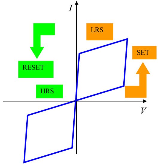
Figure 1. The schematic representation of a current-voltage dependence on a memristor.
Since during the reversible insulator-metal process the conductance of the memristor is modulated in time, i.e., it increases during the transition from HRS to LRS and decreases in the transition from HRS to LRS, any memristor can be seen as an artificial synapse [6] and, thus, many applications in the new field of neuromorphic computing can be envisaged. The equation of any memristor is given as follows:

where γ(t) is a continuous time-dependent function with values in the range [0, 1]. The function γ(t) reaches its maximum and minimum values, of 1 and 0, when R = RON (LRS) and R = ROFF (HRS), respectively. γ(t) is considered as a linear function of the flux linkage.
A recent review about memristors and their applications as memories and synapses can be found in [1][7]. Furthermore, the majority of memristors are oxide memristors, in which the reversible transformation from HRS to LRS is due to conduction filaments formed inside the oxide; for this reason, they are also termed as filament memristors.
In the Set process, pairs of oxygen vacancies (anions) are created inside the oxide due to the impact ionization process: OL → VO2+ + Oi2−, where OL are the oxygen atoms in the oxide lattice, VO2+ are the oxygen vacancies and Oi2− are supplementary oxygen ions produced in the lattice. The Oi2− ions are migrating to the top electrode, while the oxygen vacancies are migrating in the opposite direction to the bottom electrode, and trap the electrons. Thus, at the bottom electrode the population of oxygen vacancies is formed and is propagating to the top electrode, which causes the formation of tiny current filaments, hence providing conduction in the oxide and, as a consequence, the transition from an insulating to a conduction state (i.e., the transition from HRS to LRS). In the Reset process, the large densities of current filaments are cancelling oxygen vacancies via Joule heating: VO2+ + Oi2− → OL. Therefore, we have the inverse transition from LRS to HRS. These processes are depicted schematically in Figure 2.
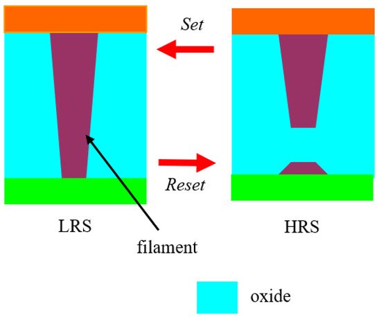
Figure 2. Schematic representation of the filament memristor and its states.
Soon after the discovery of the memristor, it was used as a high-frequency switch [8]. This was a logical step, since memristors have low RON (in the range of 10–100 Ω), while ROFF is in order of tens or hundreds of MΩ. The oxide memristor is embedded in a planar waveguide termed coplanar waveguide (CPW), consisting in three metallic electrodes separated by two gaps, with the central conductor being the signal line and the outer electrodes being the ground planes; all the three electrodes are deposited on an insulator substrate. The CPW line has both input and output impedances of 50 Ω (standard reference impedance for microwave circuits). In the case of the microwave memristor switch described in [8], the substrate is a 525 μm-thick high-resistivity (HR, with resistivity of 1000 Ω·cm) silicon (Si) wafer having a 200 nm-thick silicon dioxide (SiO2) layer grown over it, such that the memristor is isolated from the substrate containing surface charges. The memristor is a MIM-like device, having two dissimilar metallic electrodes: the bottom electrode is Ti (5 nm)/Pt (20 nm), while the top electrode is Ta (30 nm)/Pt (200 nm). The oxide is amorphous Ta2O5 having the thickness of 7 nm, with a high density of oxygen vacancies. This memristor is integrated in the central electrode of the CPW as it is shown in Figure 3. The Set pulse has an amplitude of +2 V and a duration of 105 ps, while the Reset pulse has an amplitude of +3.3 V and a duration of 120 ps. The ON- and OFF-state are evidenced by the sub-ns time response, meaning that the memristor works as a switch up to 20 GHz.
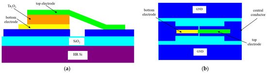
Figure 3. The microwave filament memristor in coplanar waveguide (CPW) technology: (a) cross-section; (b) top-view.
Further developed memristors based on monolayers, such as MoS2 or h-BN, rely upon the concepts described above, i.e., the monolayer is embedded in the central conductor, the ON resistance is kept low (at 10–20 Ω), and the results show that the monolayer memristors are very good microwave switches, having low insertion loss (<2 dB) and high isolation (between −25 and −30 dB); moreover, they are able of high-power handling [9][10]. The first experimental results show that these memristors are filament memristors, even if they are monolayers.
This entry is adapted from the peer-reviewed paper 10.3390/nano11030625
References
- Dragoman, M.; Dragoman, D. The Electronics at Atomic Scale beyond CMOS; Springer: Cham, Switzerland, 2021.
- Rebeiz, G. RF Mems: Theory, Design and Technology; Wiley: Hoboken, NJ, USA, 2004.
- Ziaei, A.; Charles, M.; Le Baillif, M.; Xavier, S.; Caillard, A.; Cojocaru, C.S. Capacitive and ohmic RF NEMS switches based on vertical carbon nanotubes. Int. J. Microw. Wirel. Technol. 2010, 2, 433–440.
- Dragoman, M.; Dragoman, D. 2D Nanoelectronics Physics and Devices of Atomically Thin Materials; Springer: Cham, Switzerland, 2017.
- Strukov, D.B.; Snider, G.S.; Stewart, D.R.; Williams, R.S. The missing memristor found. Nature 2008, 453, 80–83.
- Jo, S.H.; Chang, T.; Ebong, I.; Bhadviya, B.B.; Mazumder, P.; Lu, W. Nanoscale memristor device as synapse in neuromorphic systems. Nano Lett. 2010, 10, 1297–1301.
- Slesazeck, S.; Mikolajick, T. Nanoscale resistive switching memory devices: A review. Nanotechnology 2019, 30, 352003.
- Torrezan, A.C.; Strachan, J.P.; Medeiros-Ribeiro, G.; Williams, R.S. Sub-nanosecond switching of a tantalum oxide memristor. Nanotechnology 2011, 22, 485203.
- Kim, M.; Ge, R.; Wu, X.; Lan, X.; Tice, J.; Lee, J.C.; Akinwande, D. Zero-static power radio-frequency switches based on MoS2 atomristors. Nat. Comm. 2018, 9, 2524.
- Kim, M.; Pallecchi, E.; Ge, R.; Wu, X.; Ducournau, G.; Lee, J.C.; Happy, H.; Akinwande, D. Analogue switches made from boron nitride monolayers for application in 5G and terahertz communication systems. Nat. Elect. 2020, 3, 479–485.