A Transparent Conducting Oxides (TCO) is a wide band-gap semiconductor that has high concentration of free electrons in its conduction band.
- chemical vapor synthesis
- hydrogen-sensing
- indium-doped zinc oxide
- indium tin oxide
1. Overview of Transparent Conducting Oxides (TCO's)
A TCO is a wide band-gap semiconductor that has high concentration of free electrons in its conduction band. These arise either from defects in the material or from extrinsic dopants, the impurity levels of which lie near the conduction band edge. The high-electron-carrier concentration causes absorption of electromagnetic radiation in both the visible and infrared portions of the spectrum for the present purposes, with the former being more important. As a TCO must necessarily represent a compromise between electrical conductivity and optical transmittance, a careful balance between the properties is required [1].
Generally, TCOs are metal oxides with high optical transmittance and high electrical conductivity [2]. They are also referred to as wide-bandgap oxide semiconductors (band gap > 3.2eV). These materials have high optical transmission at visible wavelengths (400–700 nm) and electrical conductivity close to that of metals, which is often induced by doping with other elements. They also reflect the near infrared and infrared wavelengths. Since the bandgaps of these materials lie in the ultraviolet wavelength region they hardly absorb visible light; thus, they appear to be transparent to the human eye [3].
Transparent conducting oxides (TCOs) are used in a wide range of applications, including low-e windows, transparent contacts for solar cells, optoelectronic devices, flat panel displays, liquid crystal devices, touch screens, electromagnetic interference (EMI) shielding, and automobile window deicing and defogging. Low cost, high durability and being non-toxic make ZnO an attractive alternative to the commonly used ITO. ZnO has a direct and wide band gap in the near-UV spectral region and a large free-exciton binding energy so that excitonic emission processes can persist at or even above room temperature. One of the key challenges in developing ZnO-based TCOs is investigating the best metal dopants and the optimal dopant contents in order to achieve the highest electrical conductivity. Unlike in SnO2 and In2O3-based TCOs, efficient doping of group III elements into the ZnO structure could decrease the resistivity significantly, potentially realizing a future low cost TCO for electronic and optoelectronic applications [4][5].
2. Opto-Electrical Properties of TCOs
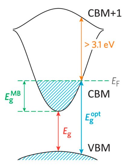
For electrical conduction to occur within a semiconductor material, ground state electrons must be excited from the valence band to the conduction band minimum (CBM). A wider band gap requires a higher-energy photon. Therefore, widening the band gap (i.e., Eg > 3.0 eV) in a material permits transparency to the visible portion of the spectrum by placing a greater separation between the valance band maximum (VBM) and CBM of the material, thus decreasing the probability of exciting an electron into conduction [6]. TCOs have been developed by doping materials in order to facilitate the charge carrier generation within the structure. In the description of the band model as shown in Figure 1, there is an important difference between the fundamental band gap (i.e., the energy separation of the Evb and Ecb; an intrinsic property of the material) and the optical band gap (an extrinsic property), which corresponds to the lowest energy allowed for an optical transition.

Figure 1. Diagram of the optical widening by the effect of the Moss–Burstein shift. Reproduced from Ref. [6], an open access article.
The optical band gap determines the transparency of a material which is important in TCO applications. In order to achieve n-type conducting properties, electrons are injected from a nearby defect donor level directly into the conduction band. The point defects in a metal oxide crystal, such as oxygen vacancies, proton or metal interstitials and certain substitutional defects, effectively create an excess of electrons close to the defect site in n-type TCOs. If there is sufficient orbital overlap, it permits delocalization of electrons from the defect sites such that electronic states at the CBM become filled or in other words Fermi level shifts above the CBM. This leads to an effect known as the Moss–Burstein shift, which effectively widens the optical band gap [3].
Since the Moss–Burstein shift is:
where Eg is the fundamental energy gap separating the VBM and CBM, Eoptg is the optical band gap corresponding to the smallest allowed optical transition from the VB to the CB, EMBg is the Moss–Burstein shift and EF is the Fermi level. Thus, lattice defects in TCOs can simultaneously promote both electrical conductivity and optical transparency. Apart from the Moss–Burstein shift, the fundamental band gap is tapered due to the band gap narrowing effect which led by exchange interactions in the free-electron gas and electrostatic interactions between free electrons and ionized impurities [7]. The optical band gap is a key aspect in designing a TCO. However, the CBM depth or electron affinity (EA), in other words the difference between valence energy and CBM which affects the “dopability” of the TCO, is also equally important in determining the conducting properties. A higher value of EA indicates greater ease of introducing charge carriers, i.e., a greater dopability [8]. A large separation (Eg > 3.0eV) between the Fermi level in the conduction band and the next electronic energy level (CBM+1) helps to prevent excitation of electrons to higher states within the conduction band, which prevents undesirable optical absorption [9].
3. Plasma-Assisted Chemical Vapor Synthesis
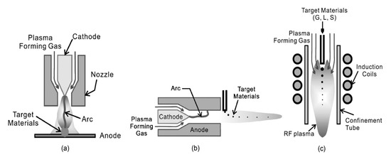
Chemical vapor synthesis involves introducing vapor phase precursors into a heated reactor and allowing vapor phase nucleation to occur in the reactor rather than depositing the product as a thin film. The precursors can be solid or liquid in nature but are introduced into the reactor as a vapor by sublimation or evaporation [10]. Chemical vapor synthesis assisted by thermal plasma involves the use of a plasma flame as the heat source and types of plasma torches are illustrated in Figure 2 [11].

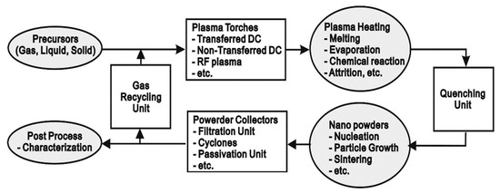
Plasma flames can facilitate vapor phase reactions by providing sufficient energy for vaporizing precursors and subsequent chemical reactions. The temperature of plasma flame generated is high enough to decompose even reactants of high vaporization temperatures into atoms and radicals, which can then react and condense to form nanosized particles when cooled by mixing with cool gas or expansion through a nozzle as shown in Figure 3.

Thermal plasma provides a high processing rate and other advantages like good control over size, shape and crystal structure as well as a clean reaction atmosphere that allows high purity products, a high quench rate to form ultra-fine powder, and a wide choice of reactants [12][13]. Compared with other methods it avoids multiple steps like in mechanical milling, sol-gel method and precipitation method and does not require a high liquid volume and surfactants that are involved in a wet chemical process. Precursors like chloride salts are commonly used in wet chemical methods but the presence of chloride ions form hard agglomerates in oxide particles and also difficult to be rinsed from the colloidal hydroxide precipitate [14].
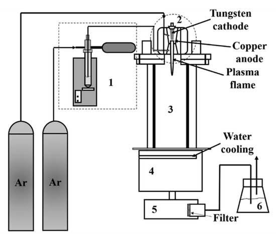
The plasma reactor system used in this work [15] for the synthesis of indium tin oxide (ITO) nanopowder consisted of a downward plasma torch, a cylindrical reactor, a powder feeding system, cooling system, powder collectors, and an off-gas scrubber, as shown in Figure 4. The plasma torch had a copper cathode and a tungsten anode. It was water-cooled and operated at atmospheric pressure. The reactor assembly consisted of a vertical stainless-steel tube, which was water-cooled, and had the dimensions of 15 cm inner diameter and 60 cm length. A graphite cylinder of 7.6 cm inner diameter and 60 cm length was placed inside the stainless-steel tube. A graphite felt filled the gap between the graphite cylinder and the stainless-steel tube. The cooling chamber consisted of two-layer stainless steel to cool the outgoing gases below 150 °C. The precursor was directly fed into the plasma gun using Ar as the carrier gas through a powder feeding system consisting of a test tube filled with the precursor powder, a motor that pushed up the test tube at a constant rate, a carrier gas line that carried the fluidized particles from the top of the particle bed in the test tube, and a vibrator. The product was collected on a Teflon coated polyester filter with a pore size of 1 µm. The off-gas scrubber used a 5% NaOH solution. More details about the experimental set-up can be found in previous publications [13][16].

Figure 4. Schematic diagram of plasma reactor system: (1) powder feeding system, (2) plasma gun, (3) reactor chamber, (4) cooling chamber, (5) powder collector, and (6) scrubber. Reproduced with permission from Ref. [15]; published by IOP Publishing, 2018.
This entry is adapted from the peer-reviewed paper 10.3390/molecules26051456
References
- Coutts, T.J.; Young, D.L.; Li, X. Characterization of transparent conducting oxides. MRS Bull. 2000, 623, 16–20.
- Granqvist, C.G.; Hultåker, A. Transparent and conducting ITO films: New developments and applications. Thin Solid Films 2002, 411, 1–5.
- DSY, J.; Peiris, N. Overview on Transparent Conducting Oxides and State of the Art of Low-cost Doped ZnO Systems. SF J. Mater. Chem. Eng. 2018, 1, 1004.
- Ellmer, K.; Klein, A.; Rech, B. Transparent Conductive Zinc Oxide; Springer: Berlin/Heidelberg, Germany, 2008; ISBN 9783540736110.
- Coutts, T.J.; Young, D.L.; Gessert, T.A. Modeling, Characterization, and Properties of Transparent Conducting Oxides. In Handbook of Transparent Conductors; Springer: Boston, MA, USA, 2011; Volume 1, pp. 51–110.
- Dixon, S.C.; Scanlon, D.O.; Carmalt, C.J.; Parkin, I.P. N-Type doped transparent conducting binary oxides: An overview. J. Mater. Chem. C 2016, 4, 6946–6961.
- Liu, Y.; Li, Y.; Zeng, H. ZnO-based transparent conductive thin films: Doping, performance, and processing. J. Nanomater. 2013, 196521, 1–9.
- Walsh, A.; Buckeridge, J.; Catlow, C.R.A.; Jackson, A.J.; Keal, T.W.; Miskufova, M.; Sherwood, P.; Shevlin, S.A.; Watkins, M.B.; Woodley, S.M.; et al. Limits to doping of wide band gap semiconductors. Chem. Mater. 2013, 25, 2924–2926.
- Freeman, A.J.; Poeppelmeier, K.R.; Mason, T.O.; Chang, R.P.H.; Marks, T.J. Chemical and thin-film strategies for new transparent conducting oxides. MRS Bull. 2000, 25, 45–51.
- Sohn, H.Y.; Ryu, T.; Choi, J.W.; Hwang, K.S.; Han, G.; Choi, Y.J.; Fang, Z.Z. The chemical vapor synthesis of inorganic nanopowders. JOM 2007, 59, 44–49.
- Seo, J.H.; Hong, B.G. Thermal plasma synthesis of nano-sized powders. Nucl. Eng. Technol. 2012, 44, 9–20.
- Ryu, T.; Sohn, H.Y.; Hwang, K.S.; Fang, Z.Z. Plasma synthesis of tungsten carbide and cobalt nanocomposite powder. J. Alloys Compd. 2009, 481, 274–277.
- Ryu, T.; Sohn, H.Y.; Hwang, K.S.; Fang, Z.Z. Plasma synthesis of tungsten carbide nanopowder from ammonium paratungstate. J. Am. Ceram. Soc. 2009, 92, 655–660.
- Wang, H.; Xu, X.; Zhang, J.; Li, C. A Cost-Effective Co-precipitation Method for Synthesizing Indium Tin Oxide Nanoparticles without Chlorine Contamination. J. Mater. Sci. Technol. 2010, 26, 1037–1040.
- Murali, A.; Sohn, H.Y. Plasma-assisted chemical vapor synthesis of indium tin oxide (ITO) nanopowder and hydrogen-sensing property of ITO thin film. Mater. Res. Express 2018, 5, 065045.
- Lan, Y.P.; Sohn, H.Y.; Mohassab, Y.; Liu, Q.; Xu, B. Properties of stable nonstoichiometric nanoceria produced by thermal plasma. J. Nanoparticle Res. 2017, 19, 281.
