Your browser does not fully support modern features. Please upgrade for a smoother experience.
Please note this is an old version of this entry, which may differ significantly from the current revision.
In this review, we will discuss the development in the LHP-based functional devices in recent years. After a brief presentation of the LHP's properties, we will focus on the functional devices including lasers, photodetectors, and modulators. Then the fabrication of the LHP-based devices will be presented, which is followed by the summary and outlook.
- Lead Halide Perovskites Material
- Laser Photodetector Modulator
1. Introduction
The three-dimensional (3D) lead halide perovskites (LHPs) are enjoying rapid developments as novel opto-electronic materials since their emergence in photovoltaic applications in 2009. LHPs belong to the larger material family of metal halide perovskites (MHPs), which exhibit very similar structure with CaTiO3 and could be generally represented by the formula of ABX3. X represents the halide anion forming octahedrons, which could be Cl−, Br−, and I− [1]. B represents cation locating in the center of octahedron, which could be Pb2+, Sn2+, and Ge2+ in the more generalized cases of MHPs [2,3,4] but restricted to be Pb2+ for LHPs. A represents the cation locating in the vacancy of neighboring octahedron cages, which could be either organic or inorganics: the inorganic examples include Cs+ [5], while the organic examples include the methylammonium [6,7], formamidinium [8,9], and recently discovered methylhydrazinium [10,11]. It is expected that inorganic counterparts generally maintain better chemical stability than their organic counterparts [12]. When specified to the 3D LHPs, the materials have advantageous properties from more than one aspect, and people are eager to utilize them as working materials in various opto-electronic devices. In addition to solar cells [1,13], the materials are also utilized in lasers [7,14], light emitting diodes (LEDs) [15,16,17], photodetectors [18,19,20], modulators [21,22,23], and so on. Moreover, the materials, especially those with bromides, are found to exhibit outstanding nonlinear properties [10,24,25,26,27], thus demonstrating promising potential in applications such as imaging, optical limiting, and frequency conversion. Currently, people are incorporating the LHPs into waveguides and micro optical cavities, so as to further miniaturize the LHP-based devices. These efforts are leading to the emergence of integrated photonic/optical systems centering LHPs, which will play a significant role in next-generation opto-electronic applications, resulting in devices not only frequently used in the field of scientific research but also that of consumer electronics. In Figure 1, the crystalline structure of LHP is presented in the center, which is surrounded by examples of potential applications for the LHP-based devices.
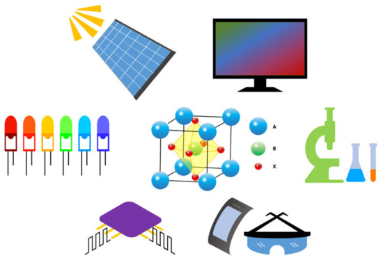
Figure 1. Lead halide perovskites (LHPs) and their potential applications in various fields, including photovoltaic, illumination, communication, wearable devices, chemical test, and high-resolution display.
In addition to the prosperity of LHP material, novel opto-electronic materials including the atomically thin two-dimensional materials (2D) and one-dimensional (1D) materials are also rapidly growing. These materials, each with their unique properties in certain aspects, are also at the center of attention in the research community. LHPs, along with other materials, are all building blocks to construct devices. To some extent, people are free to choose from this “material bank” to fabricate devices and achieve better performances. In most cases, it is quite rigorous that a single species of material could cover all the application demands and introduce no impediments at the same time. On the other hand, it is more practical to combine different materials into the device and make them collaborate such that the advantages from the participants could be utilized, and the shortages could be made up to some extent. The LHP could be fabricated by solution-based methods and conveniently incorporated with semiconductors, metals, and polymers, making it very practical to construct LHP hybrid devices. By now, people have developed LHP hybrid devices covering lasers, photodetectors, modulators, and so on. The materials in collaboration with LHP include novel materials (for instance, graphene and 2D MoS2, etc.) and traditional materials (for instance, silicon). In these devices, the advantageous properties of participating materials are exploited, and the device performances have been improved substantially as compared to the devices made from single species of material. It is beneficial to retrospect these valuable works, which could light up more inspiration and enlightenment for future development in LHP hybrid devices.
This entry is adapted from the peer-reviewed paper 10.3390/app11041453
This entry is offline, you can click here to edit this entry!