Enormous nonlinearities in liquid crystals (LCs) have sparked intense efforts on a wide range of nonlinear optical phenomena. New materials, structures, and phenomena are setting new milestones, record-breaking performance characteristics, and interesting fundamental issues in material or optical physics, which are being constantly uncovered [1,2,3]. Advanced alignment techniques of LCs can be useful in fabrication of modern optical devices [3,4].
Anisotropic interaction between liquid crystal and the aligning surface determines the direction of the easy alignment axis of LC on the aligning surface. Director of LC coincides with the direction of the easy axis if the director is not affected by any elastic torque. The easy axis is given by azimuthal φ and polar θ angles. Alignment strength is related to anchoring energy. The anchoring energy comprises two contributions, which are related to the director tilt in the azimuthal plane (azimuthal anchoring energy, Wφ) and the tilt in the polar plane (polar anchoring energy, Wθ). As it turned out, Wφ can be controlled by polarized ultraviolet light if one of the substrates is spin-coated by azo dye [5]. One of the crucial technological problems is to get uniform planar or tilted alignment of LCs with the required pretilt angle and anchoring energy and high alignment stability. One of the promising non-contact alignment methods, photoalignment, can utilize the polarized light to generate anisotropy on the substrate surface, which overcomes undesired effects [6,7].
At present, surface treatment can be carried out with several approaches: rubbing with polyimide compounds [8], photoalignment [9], reactive monomers [10,11], and silicon oxide evaporation [12]. High alignment quality and defect-free alignment surfaces make the photoalignment technology attractive for further investigation [13].
Photoalignment technology provides effective control of main anchoring parameters: easy alignment axis, pretilt angle, and anchoring energy [14]. Consider main advantages of photoalignment over the rubbing technology. First, non-contact technology does not produce electrostatic charges or mechanical defects on the substrates. Secondly, elimination of undesired defects enables researchers to develop advanced photonic applications of liquid crystals, which are impossible with the rubbing technique.
2. Applications of Photoalignment in Device Development
2.1. Simulation-Based Performance of Optically Rewritable e-paper
Optical properties of LCs can be easily tuned if its layer is placed in electrical or magnetic field. The corresponding response to external fields definitely leads to reflective or transmittive characteristics of the display. However, what if the intensity of the irradiated light will change the anchoring properties of the TN film? If so, it enables us to produce light-generated images, which is the concept of optically rewritable electronic paper (ORW e-paper). There exist many other reflective e-paper-developing technologies, where high white state reflectance (%) is critical. For example, electrophoretic (E-Ink, ≈40%), electrowetting (Liquavista, ≈50%), cholesteric liquid crystal (Kent Displays Inc., ≈30%), electrochromic (NTerra Inc., ≈45%, DIC, ≈65%), micro-electromechanical interference (Qualcomm Inc., ≈25%), and liquid powder (Bridgestone, ≈40%). Nonetheless, reflective characteristics of the mentioned technologies are lower than those of a white paper sheet (over 80%) [
36].
Below, we describe potential characteristics of e-paper, which were obtained by using the software MOUSE-LCD (developed by the Hong Kong University of Science and Technology and the Saratov State University) [
37,
38,
39], which enables us to elaborate different cell structures, boundary conditions, and LC compounds. In particular, by changing boundary conditions on SD1-coated substrate, a 2D image can be simulated. In order to compute reflective characteristics and contrast ratio, 8 × 8 transfer matrix approach can be used.
Geometric representation of the TN cell with a reflective polarizer film is shown in a. Some technological aspects in fabrication of such cells are discussed in [
40,
41,
42]. High optical performance in the reflective mode can be achieved if the phase retardation is Δ
nd, where Δ
n is the birefringence and
d is the cell gap. As was mentioned above, flexible (polyethersulfone, PES) substrates are indispensable in the ORW concept. Consideration of flat surfaces significantly simplifies the corresponding computations.
Figure 5. (Color online) (
a) Schematic representation of twisted nematic liquid crystal cell (
d = 6.85 μm). (
b) Device structure of optically rewritable electronic paper (ORW e-paper) [
43].
A schematic cross-sectional view showing a reflective-type liquid crystal display device is depicted in b. In an attempt to obtain more realistic results, it was necessary to consider dispersion effects. The following elastic moduli were used: K1 = 1.3 × 10⁻⁶, K2 = 6.5 × 10⁻⁷, K3 = 1.95 × 10⁻⁶ dyn in our computations. All these parameters enabled us to calculate the static director distribution in the LC layer by numerical integration of the Euler equation.
The obtained dependence of the normalized reflectance versus the twist angle indicates its saturation trend ().The simulated image in the insert of showed a very close background color to the result of the experimental studies [
40,
44].
Figure 6. (Color online) Normalized reflectance of ORW e-paper versus the twist angle. Insert: the generated image includes maximum and minimum of the normalized reflectance [
43].
The achieved values of the normalized reflectance coefficients ranged from ≈0.03 to 0.43, which is higher or comparable with other commercial technologies. The obtained value of the contrast ratio achieved 10:1, which is also consistent with other studies. A significant advantage of ORW e-paper is that it does not require formation of static charges and electrodes. Our calculations also indicate that angular dependence of the reflectance coefficient is homogeneous within a wide range of viewing angles.
2.2. Optically Driven Color LC Displays
In spite of the conventional LC displays with backlight to obtain different combinations of three primary colors (red, green, and blue), optically driven LC displays do not have backlight. When some areas of the display are in a bright state, it means that the director of LCs changes by π/2 with respect to the alignment direction provided by optically active layer. If other areas have dark states, it means that the director is twisted by an angle smaller than π/2 (a). It is important to align the position of twist and planar domains carefully with color arrays. On the basis of the rewritability of optically active alignment layer, image can be easily rewritten with the patterned image mask under polarized light. This method can be applied to transmittive display with transparent polarizer or reflective display with mirror or reflective polarizer below the color filter.
Figure 7. (
a) Schematic representation of optically driven LCD. (
b) Optically driven LCD with patterned reflective paint [
45].
Reflective painted background coating serves as a patterned color array and reflector to create colored display cell. Consider, e.g., red color transmitting through twist regions (bright state) is reflected back from the reflective paint, as pictured in b. Other colors can also be obtained with the same approach.
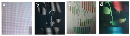
One apparent way to generate colors in optically driven LCD is to use color filter. The image demonstrated in a shows patterned (gridded map) color filter. The flower image depicted in b was obtained without color filter. Here, the easy axis of LC for the optically active alignment layer changed under the exposure light, displaying the flower pattern in black and white colors. When a color filter and a transparent polarizer were added to the device, it enabled the light to go through the display (c). If the reflective polarizer is placed behind the front surface of the display, the light will go passes through the display and will be reflected back, but will not leave the device. The corresponding image of reflective mode is shown in d.
Figure 8. Flower images of color optically driven LCDs: (
a) gridded color map; (
b) flower pattern without color filter; (
c,
d) transmissive and reflective modes with color filter, respectively (each colored line width ≈ 1 mm) [
45].
Another method to assemble reflective color optically driven LCDs is to use reflective paint as patterned color array. Consider patterned reflective paint, which was assembled to obtained different colors, as shown in a. Furthermore, three characters, namely, “S”, “K”, and “L”, depicting red, blue, and green colors, respectively, are shown in b. Letter “H” includes red, blue, and green colors (b).
Figure 9. (
a) Patterned colors: each color line ≈ 1 mm. (
b) Colored images of letters, obtained by using reflective paint [
45].
Application of color filters can be successfully used in fabrication of optically driven color displays. Method of reflective paint application is simple and effective, and it does not require any other reflectors. The methods that we considered were tested with color optically driven LCD demos exhibiting 21% National Television Standards Committee (NTSC) color standard. It is believed that all these findings can improve optically driven display performance and will trigger applications in flexible full-color display devices.
2.3. Dammann Gratings
Potential applications of diffractive elements with high-performance optical characteristics (excellent performance and compact size) are of growing interest among many researchers [
46,
47,
48,
49] because they provide an effective method for design and fabrication of compact and fast-switchable diffractive optical elements.
Dammann gratings (DGs) are binary phase gratings that are used to produce one- or two-dimensional array of equal-intensity light spots. The idea behind the DGs is to obtain multiple images from one input object for optical lithography [
50]. After this original publication in 1971, many other interesting applications have been proposed, e.g., laser beam summation [
51], optical interconnections [
52], 3D optical imaging [
53], 3D lattice structure generation [
54], and optical communication [
55].
Circular Dammann gratings (CDGs), which generate concentric and equal-intensity rings, have many applications in image coding [
56,
57], beam shaping [
58], vortex manipulation [
59,
60] and precise measurements [
61,
62]. Much effort has been expended to enhance the efficiency and the uniformity of CDGs by profile optimization [
63,
64,
65]. However, realization of tunable CDGs has been accomplished only in recent years.
Modification of the grating structure enables us to observe array of diffractive orders with different vortex phase distributions. In order fabricate such DGs, a conventional method can be used—mask preparation by using electron beam (or laser), etching substrate with plasma, reactive ion, or wet chemical. The advantage of this fabrication method is high resolution up to sub-micrometers, but the disadvantage is that the grating is fixed with no tunability and the fabrication process is tedious.
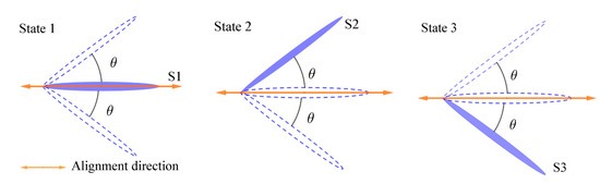
In order to obtain high switching time, researchers suggested the use of electrically suppressed helix (ESH) mode of ferroelectric liquid crystals (FLCs) [
66]. Consider the details of ESH mode, which is characterized by good alignment quality and fast response time at low driving voltages. The working principle of the ESH FLC is illustrated in . When the voltage is not applied to the cell, the FLC helix is aligned along direction S1. Consequently, the molecules will form helical structure, which is represented by State 1.
Figure 10. Top view to illustrate the ferroelectric liquid crystal (FLC) molecule orientation. State 1 represents the no-applied-electric-field state, and State 2 and 3 represent the two different states with different electric field polarities.
When electric field (>0.5 V/μm) is applied to the FLC cell, the helical structure becomes suppressed, and FLC molecules will switch around the cone surface, as shown in (States 2 and 3). Different switching directions are explained by the polarity of the electric field. Axes S2 and S3 can be considered as the slow optical axis of the FLC-based wave-plate [
67]. Angle θ is the tilt angle, which is determined by the FLC compound.
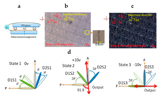
In order to observe ESH FLC mode, polarizer (P) and analyzer (a) are set on the two sides of the FLC cell. In our design, the polarizer (P) and analyzer (A) are oriented along directions, which characterize State 3 (two possible orientations). According to the configuration represented by State 3, the transmitted light by the first polarizer will have the polarization plane parallel to the optical axis of the FLC waveplate. It means that polarization plane will not be changed after the FLC DG, as shown in d. All light will be blocked by the analyzer. Thus, State 3 shows a non-diffractive (dark) state. This phenomenon can be observed in c, where the two domains are in the dark state.
Figure 11. (
a) Structure of the FLC Dammann grating; (
b) diffractive state under crossed polarizer and analyzer (microscopic photo); (
c) microscopic photo of the electrically suppressed helix (ESH) FLC Dammann grating (DG) in the non-diffractive state under crossed polarizer and analyzer; (
d) illustration of molecular orientation and the output polarization plane in different states for two types of domains [
67].
Consider the output of State 2. The angle between the molecules and the polarizer direction is π/4. The phase retardation of the FLC waveplate is close to be half-wave condition, which will rotate the polarization plane by π/2 (d). In this case, light will be transmitted through the analyzer. This can be verified by the micrograph shown in b, where all domains are bright.
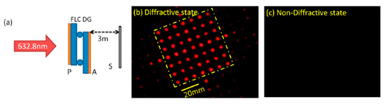
In order to demonstrate the performance of the DG, the optical setup, which is depicted in a, can be used. A light beam from a He–Ne laser with the wavelength of 632.8 nm was used to transmit the light through the assembled FLC DG, as pictured in . Electric field between the indium tin oxide coated substrates was controlled by the signal generator.
Figure 12. (
a) Optical setup for demonstration of the diffraction performance in the DG; (
b) observation of the diffractive state; (
c) non-diffractive state [
67].
Upon reversing the electric field polarity between +10 V and −10 V, the grating can be switched between diffractive and non-diffractive states. The projected diffraction spots (b,c) can be observed on the screen (S) behind the DG. It can be seen from b that the diffractive state of the DG projected 7×7 orders (dashed yellow square). The measured diffraction efficiency was 75.4%.
Circular DGs (CDGs) have also been extensively studied [
54,
60,
68]. Circular structure of the substrate can be achieved if a two-step photoalignment technique is applied [
69]. Application of FLCs as functional materials of the CDG enables achievement of submillisecond electro-optic response.
A two-step exposure technique was used to assemble binary eight-order FLC CDG with perpendicular alignment of even and odd zones. For the CDG with multi-level or even continuous modulation, it can be achieved by multiple step exposure process, since the resolution of FLC photoalignment is in the sub-micron scale [
70]. To transfer the CDG pattern to the alignment layer of FLC, a two-step exposure process must be implemented with the azo dye as the aligning layer. The aligning layer provides the alignment of FLC helix perpendicular to the polarization plane of the incident light (a). Linearly polarized UV light with uniform intensity (central wavelength is 365 nm and
I = 5.5 mW/cm
2) generates the first alignment direction (a). Then, the alignment direction of SD1 must be rotated by π/2 to create other perpendicularly aligned domains on the same substrate (see b). The illuminated substrate can be utilized to assemble cell with asymmetric configuration, in which surface aligning layer is only on one substrate, as shown in c [
71].
Figure 13. Two-step exposure technique of patterned alignment for FLC circular DG (CDG): (a) exposure of polarized UV on the SD1 substrate; (b) exposure of SD1 substrate with the mask; (c) FLC CDG cell with a single-side alignment.
Then, the FLC material FD4004N (DIC, Japan) was filled into the prepared cell. The FLC material FD4004N had the following phase transition scheme: SmC* → SmA → N* → Iso at the temperatures of 72 °C, 85 °C, and 105 °C, respectively. The FLC helix pitch, spontaneous polarization, and the tilt angle were equal to
P0 =350 nm,
PS ≈ 61 nC/cm
2, and tilt angle
θ ≈ 22.05°, respectively, at room temperature. In order to control the cell gap and maintain the optimized contrast between odd and even zones, we used 9 µm thick spacers between the substrates. Given the fact that the exposure dosage determined the photoinduced anchoring of SD1 layer, the exposure time was optimized for alignment quality [
5]. Considering the thickness and the elastic property of FLC material, the UV dosage of 10 J/cm
2 was irradiated for creating the optimal aligning condition. In this case, a proper balance was achieved between the anchoring energy of alignment layer and elastic energy of the helix in cells with thickness much larger than helical pitch. The fabricated device had perpendicular helix axes in the adjacent areas.
When the half-wave condition was satisfied, π-phase shift occurred for the light propagating between odd and even domains. All these conditions enabled observation far-field diffraction patterns exhibiting equal-intensity rings (see a). Diffraction intensity profile up to the eighth order can be acquired by photodetector, and the corresponding result is shown in b.
Figure 14. Observation of diffraction rings provided by FLC CDG: (
a) the far-field diffraction patterns and (
b) visualization of light intensity profiles [
71].
Circular DG can produce equal-intensity nested diffraction rings. Accordingly, our further discussion is given in terms of diffraction efficiency (a value that expresses the extent to which energy can be obtained from diffracted light with respect to the energy of the incident light) and uniformity. Given that the half-wave condition is satisfied, which is phase retardation different between odd and even zones matching 5λ/2, the efficiency and uniformity are expected to be high. The diffraction efficiency of the CDG is defined as η=ΣIn/Iout
, where ΣIn is the total intensity of all diffraction peaks and Iout
is the output intensity. The measured magnitude of the diffraction efficiency was shown to be 84.5%, which correlated with the theoretical limits.
The response time can be measured by detecting the intensity of the diffractive orders. The switching-on time was measured when the transmittance of the diffractive orders increased from 10% to 90%, and the switching-off time corresponded to from 90% to 10%. When the magnitude of the electric field was 4.3 V/µm, the response time for both times τON
and τOFF
was about 64 µs. This, inherent spontaneous polarization of FLCs make it possible to achieve submillisecond response time.
The stabilized by azo dye FLC film has high optical quality and enhanced stability. Proper treatment and irradiation doses for two-step photoalignment open the opportunity for the development of optical devices with record-breaking characteristics.