We give a systematic overview of compositional engineering by distinguishing the different defect-reducing mechanisms. Doping effects are divided into influences on: (1) crystallization; (2) lattice properties. Incorporation of dopant influences the lattice properties by: (a) lattice strain relaxation; (b) chemical bonding enhancement; (c) band gap tuning. The intrinsic lattice strain in undoped perovskite was shown to induce vacancy formation. The incorporation of smaller ions, such as Cl, F and Cd, increases the energy for vacancy formation. Zn doping is reported to induce strain relaxation but also to enhance the chemical bonding. The combination of computational studies using (DFT) calculations quantifying and qualifying the defect-reducing propensities of different dopants with experimental studies is essential for a deeper understanding and unraveling insights, such as the dynamics of iodine vacancies and the photochemistry of the iodine interstitials, and can eventually lead to a more rational approach in the search for optimal photovoltaic materials.
- solar energy
- semiconductor
- light harvesting
- charge generation
- photovoltaics
- optimization
- voltage loss
- thin film materials
- stabilization
- doping
Compositional engineering has become an attractive approach to optimize perovskite structure because of the advantage of directly tailoring other intrinsic material properties, which enables higher-quality perovskite with enhanced photovoltaic performances. Reference [1] contains a condensed historic representation of compositional changes related to record perovskite devices (see Table 2 of reference [1]). We can distinguish between two types of additives: Inorganic (metal cations and inorganic acids) and organic additives (small molecules, polymers, and fullerenes). Most additives can control the crystallization of perovskite in some way and, therefore, enhance stability [2]. However, organic molecules generally only passivate defect states at the surface and not do not alter intrinsic material properties, while the bulk trap density might be reduced by the incorporation of inorganic molecules into the lattice. In literature a variety of dopant- effects that enhance perovskite performance are reported [1], [2], [3], [4], [5], [6], [7], [8], [9], [10], , which can be divided into influences on the crystallization and influence on the intrinsic lattice properties. Most effects described in literature are still not well-explained making rational compositional tailoring challenging. Here, current literature on Zn(II) and several other inorganic dopants are reviewed with the aim to obtain a more mechanistic picture on how dopants affect different properties and control the defect density.
A considerable amount of literature has been published on the use of inorganic dopants that improve photovoltaic performance of perovskite materials and many attribute this to the improved crystallization of doped perovskite [1], [3], [4], [5]. While the enhanced crystallization mechanisms do not seem to be fully understood, we review here several studies on dopants that effectively improve crystallization, leading to larger crystal domains and reduced defect density, and identify mechanisms behind this dopant effect.
Wang et al. discovered that Al3+, at low concentrations (<0.3%), facilitates crystallization of MAPbI3, and specifically enhanced the growth of the (hh0) crystal plane . This was ascribed to reduced micro-strain in the lattice during the crystallization process, resulting in better oriented crystalline domains and consequently a reduced density of defects. Crystallography and mass spectrometry revealed that Al3+ was not significantly incorporated in the lattice, which is expected from the ionic radius (53 pm and 199 pm for Al and Pb, respectively). Crystal defects that potentially occur in the form of terraces are reduced via a selective growth of these terraces induced by Al3+.
Unlike Al3+, Zn2+-ions have been proven to be incorporated at the lattice B-site, replacing lead ions. Chen et al. argued that this incorporation leads to better crystallization of MAPbI3 perovskite [6]. Using X-ray diffraction (XRD) they showed successful doping of the perovskite and with attenuated total reflectance Fourier transform infrared spectroscopy (ATR-FTIR), they demonstrated that the interaction of the Zn2+ and MA ions are stronger in comparison to the Pb-MA interaction. Upon 0.1% Zn2+ doping of MAPbI3, photovoltaic performances were increased the most. This was attributed to higher chemical interaction and coordination between Zn2+ and anions, and the organic group, which makes the doped system tend to grow into larger grains. They also observed an over-doping effect for high Zn2+ concentration, which was believed to result in the accumulation of bigger grain seeds on the previous small grain seeds affecting the general coverage and therefore reducing the photovoltaic performances.
In contrast to these studies, other work shows that the relation between optoelectronic quality and the orientation and size of crystalline domains must be interpreted with caution. Muscarella et al. (2019) used electron back-scattered diffraction (EBSD), which has higher spatial resolution than the conventional XRD and scanning electron microscopy (SEM) methods, to obtain crystallographic parameters [6]. They correlated the results with local photoluminescence properties. The PL and carrier lifetimes did not show any dependence on grain size or orientation. They argued that the contrasting findings with previous studies can be explained by the following: First, morphological clusters observed in SEM and real crystallographic grains are often misinterpreted, clusters seen in SEM can be wrongly assigned to grains. Secondly, the chemical additives that create enlarged grains and preferential orientation can also passivate defects or grains.
Also Bowman et al. (2019) showed that zinc does not necessarily influence the crystal grain size or orientation but can aid homogeneous incorporation of elements [8]. Lead-tin based perovskite cells were fabricated employing different concentrations of ZnI2 precursor and from the chemical spatial distribution mapping of the elements (by using STEM/EDX = Scanning transmission electron microscopy / Energy-dispersive X-ray spectroscopy), as shown in Figure 1, it was observed that Zn doping leads to more homogeneously distributed Sn through the films (Figure 1b). The majority of the Zn localizes along the bottom of the film (Figure 1c) and, therefore, they proposed that high doping concentration can form an insulating layer. This also explained the current and voltage enhancement for the 1% and 2% ZnI2 doping devices and the decreasing device performances at 10% doping. The XRD results revealed a small increase in the lattice parameter so that it is expected that Zn is incorporated in small amount but that the structure is not altered nor its grain sizes. They speculated on the role of Zn as an active dopant, as suggested by Saidaminov et al. [4] and as additive assisting and seeding the growth of higher-quality grains that are chemically more homogeneous.
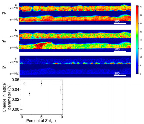
Figure 1. Distribution of elements of FA (Pb0.5Sn0.5)I3 with and without 5 % ZnI2 added measured by STEM/EDX. (a) Pb. (b) Sn. (c) Zn. (d) Change in lattice parameter with doping content. Reproduced with permission from ACS Energy Lett. 2019, 4, 2301–2307. Reference [8].
When perovskite material is tolerant to the inclusion of extrinsic dopant, additional passivating effects are observed. Here, we discuss several dopants that are able to incorporate on either the A, B, X-site or at interstitials and the subsequent influence on the lattice. The tolerance for the inclusion of foreign atoms by the perovskite lattice depends on the ionic radius. Small amounts of extrinsic doping at the A, B, X sites in the perovskite crystal can lead to increased disorder if the radius is either too large or too small. These lattice distortions affect the phase stability of the perovskite as empirically described by the Goldschmidt tolerance factor:
where r are the ionic radii and 0.8 < t < 1 to maintain the 3D perovskite lattice, with a perfect cubic base at ideal 1. For MAPbI3 the reported factor ranges between 0.92–0.95. The incorporation of Zn at the B-site has been frequently reported and can also be expected from the calculated tolerance factor of 1.05 for MAZnI3 [1]. Shai et al. argued that the incorporation of Zn(II) in MAPbI3-xClx crystals caused the lattice to shrink, they observed contraction of BX6 octahedron, which is beneficial to fix the A-site cation and relax the lattice strain [4]. This also promoted the formation of ordered and uniform perovskite crystal with tetragonal structure. They ascribed the formation of more stable perovskite to the increased electron-donating ability at the B site, creating stronger B-site–X-site interactions.
Chemical bond enhancement can also be achieved through doping with more electronegative halides. Li et al. fabricated a triple-cation perovskite (Cs0.05FA0.54MA0.41)Pb(I0.98Br0.02)3 and used several halides for doping, NaX (X = I, Br, Cl or F), in a two-step solution process [8]. All alkali halides improved the quality of the perovskite, with the fluoride-containing material (0.1%) giving the best performance. Time-resolved PL showed increased carrier lifetimes implying that non-radiative recombination is suppressed. The increased electronegativity of the fluoride anion was argued to result in a stronger ionic bond with Pb and in formation of a hydrogen bond with FA ions, leading to stabilizing of local structure and inhibiting mobilization of ions (I and MA/FA). Hydrogen bonding between the NH of the organic ion and the F ion was confirmed by 1H-nuclear magnetic resonance (NMR). The F ions did mainly occupy the surface and grain boundaries. In contrast to the other ions, devices with F− ions exhibit negligible J-V hysteresis, indicating that the chemical bond enhancement with F immobilizes the counter ions. The stabilization reported by Shai et al. resulting from lattice shrinking can be explained by the strain in the pristine perovskite lattice. Lattice strain in MAPbI3 was first observed by Huang et al. in high-temperature annealed thin films MAPbI3 perovskite [9]. Using XRD and temperature-dependent conductivity measurements, they correlated ion migration to increased lattice strain. Saidaminov et al. speculated that lattice strain is at the origin of vacancy formation [3]. DFT calculations showed that the formation energy of lead iodine vacancies was increased upon replacing FA and I with the smaller Cs/MA and Br.
They argued that if the size of the A cation does not match the lead halide octahedral cage, strain will be present in the material. When local strain acts on the lattice, strain can be released through the formation of point defects or by incorporation of small ions. Especially in FAPbI3, where size mismatch is largest, this strain is likely to be reduced by point defect formation since the calculated formation energies lie close to 0 eV. The strain relaxation through the formation of vacancies has also been observed in oxide perovskites [10].[4]
Saidaminov et al. successfully incorporated Cl– into the lattice of triple-cation perovskite films (CsMAFAPbI2.55Br0.45) [4]. They observed increased long term stability and reduced superoxide generation, which indicates that Cl reduces the density of defects. Using DFT calculations, they found ∼0.3 eV increase in formation energies for iodine vacancies. Computations also showed that the Pb-X bond length decreased, as did Pb-X-Pb distortion angles. Therefore, they proposed lattice strain relaxation as reason for reduced iodine vacancies. The downside of the substitution with small halogen anions is the widening of the band gap [12]. Although incorporation might reduce non-radiative recombination, it will lower the device efficiency because of a sub-optimal band gap. Furthermore, the incorporation of Cl ions inside other perovskite lattices, such as the MAPbI3, has been unsuccessful as the energetically more favorable location is outside the lattice . In order to relax strain further at the B-site, Saidaminov et al. incorporated Cd because it is isovalent to Pb but has a smaller ionic radius. DFT calculation showed that Cd incorporation relaxes lattice strain and suppresses the formation of I vacancies by ≥0.5 eV. The Cd incorporation also increased the PL intensity of films tenfold.
Similar effects have been observed [5] upon doping with Zn(II) in combination with Cl−, the latter originating from the alkyl-ammonium additive[13] (see Figure 2).
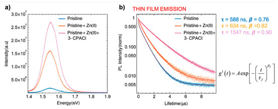
Figure 2. Characterization of MA/FA film with and without Cl− and Zn(II) dopants. (a) Relative yield of emission by time-integrated photoluminescence (PL) spectra. (b) Time-dependent PL traces with different dopants, stretched exponential fitting with function. Reproduced with permission from ACS Appl. Mater. Interfaces 2019, 11, 17555–17562. Reference [5].
Lattice distortions can also implicate the perovskite band gap (Figure 3). Prasanna et al. successfully incorporated Cs in Pb and Sn-based (FAPb/SnI3) perovskite and observed that the for tin-based films introduction of Cs at the A-site decreased the band gap; whereas in lead perovskite films, introduction of Cs was observed to increase the band gap [14]. They used grazing incidence X-ray diffraction (GIXD) measurements and revealed the incorporation of Cs has different effects in these two materials (Figure 4). The tin iodide perovskite maintains its cubic crystal structure if FA is partly substituted by Cs and the only observed change is the isotropic contraction of the lattice. However, “in the lead iodide perovskite, additional X-ray diffraction peaks are observed, indicating that the structure experiences tilting of the BX6 octahedra in addition to lattice contraction. Electronic structure calculations have shown that the VBM of perovskite material is an antibonding hybrid state of the metal s and halide p orbitals, and thus is sensitive to B-X orbital overlap (more than the CBM)” [14]. This explains the different band gap response observed in the tin iodide vs. lead iodide perovskites.
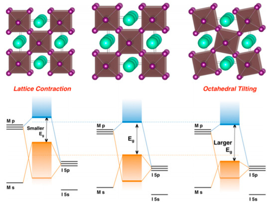
Figure 3. Perovskite lattice and energy levels of undistorted cubic phase (center), with lattice contraction (left) and with octahedral tilting (right). Reproduced with permission from J. Am. Chem. Soc. 2017, 139, 11117–11124. Reference [14].
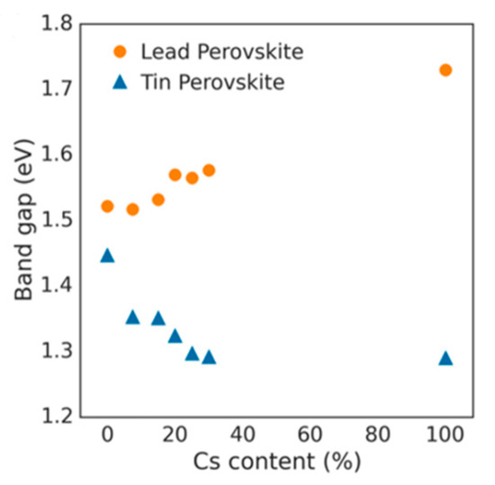
Figure 4. Optical band gap as function of cesium content for perovskites (FA1-xCsx)MI3, with M = Pb or M = Sn. Reproduced with permission from J. Am. Chem. Soc. 2017, 139, 11117–11124. Reference [14].
In the former, lattice contraction increases orbital overlap, raising the antibonding VBM and the optical band gap is decreased. “In the latter, octahedral tilting decreases orbital overlap, moving the VBM to deeper energies and causing the band gap to increase. Band gap energies were directly measured with ultraviolet and X-ray photoelectron spectroscopy (XPS) and the results support this model” [15]. Thus, for Cs doping at the A-site competing effects of octahedral tilting and lattice contraction were observed. When the X and B sites are doped, the electronic contributions of the dopant give rise to more complicated band gap interference.
Figure 5 depicts the orbital contributions of the PbI framework to the band gap of MAPbI3. “The top of the valence band consists of an Pb 6 s—I 5p * anti-bonding hybrid state of the metal s and halide p orbitals. The conduction band minimum is a hybrid of metal 6p and halide 5p orbitals with less anti-bonding and more non-bonding character” [16]. For dopants at the X-site in particular, the tuning of halogens has been frequently reported. Increasing the electron binding energies, for example from I to Br (from 5p to 4p, respectively), the band gap can be tuned from 1.5–2.3 eV by varying x in MAPb(Brx I(1−x))3 [17]. However, the band gap does not change linearly indicating increased defect densities upon Br introduction. B-site dopants are reported to infer with the conduction band. The replacement of lead with, for example, tin in MAPbI3 widens the band gap [18]. However, tin has also led to instability because of oxidation to the IV oxidation state. A recent literature review of Zn doped MAPbI3 perovskite shows that generally the 3% doping leads to the most enhanced emission intensity and lifetimes, creating PCEs between 18%–20% [1]. The band gap for low concentrations like this remains virtually unchanged [19], with valence bands shifting from −5.45 to −5.50 eV upon going from 0 to 10% Zn(II) doping. Conduction bands shifting from −3.85 to −3.91 eV in the same doping range.
We believe that a perovskite paradigm shift is needed. The perovskite solar cell research field is in strong need of a paradigm shift away from the prototypical reference material MAPbI3 (methylammonium lead tri-iodide), towards a new standard material in which MA is eliminated. Methylammonium is the weakest link in this field, as recently reported by some of the top experts [20],[23] . We have to attempt to get this message across to all researchers in the field. Still ~90% of the new papers on perovskite deal with MAPbI3. If we look at recent records, there also is a clear trend towards reducing the MA content (but so far it is not 100% eliminated) [1]. A new reference material could be formamidinium based, but not pure FAPbI3 (formamidinium lead tri-iodide). Perhaps a composite material with some bromide (~10%) Cesium and a lattice strain reducing dopant would be interesting options [3]. A new prototypical reference material for the perovskite solar cell research field is needed.
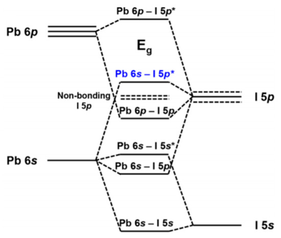
Figure 5. Band gap of MAPbI3. The orbital contributions of Pb and I. Reproduced with permission from Chem. Mater. 2016, 28, 4259–4266. Reference [16].
Table 1. The effects of doping on perovskite properties. Dopants are reported as the additive (= Add.), the content (%) is the amount that improved photoluminescence or efficiencies the most, location of incorporation is given when experimentally/computationally determined, property regulations are mostly experimentally measured, the VOC is given for the undoped and doped perovskite (ud = undoped, d = doped), together with the enhancement factor (d/ud). The year is the year the article is published, reference is given. 1 marks a computational study. It has to be noted that various device architectures and perovskite compositions are compared. The property regulation and enhancement is however a generally observed effect.
|
Add. |
[%] |
Location |
Perovskite |
Property Regulation |
VOC (ud) |
VOC (d) |
Enh. d/ud |
Year (ref) |
|
Alkali |
5 |
A-site; interstitial |
MAPbI3 |
Enlarge grain size; enhance crystallinity |
- |
- |
- |
2018 [22] |
|
Zn(II)1 |
11 |
B-site |
CsSnI3 |
Widen band gap (by 0.7 eV); change shape CBM |
- |
- |
- |
2017
|
|
ZnI2 |
1 |
B-site |
MAPbI3-xClx |
Strain relaxation; uniform crystals; chemical bond enhancement at B-X site |
1.05 |
1.08 |
1.03 |
2018 [4] |
|
ZnCl2 |
3 |
|
MAPbI3 |
Enlarged grains; improved surface morphology |
1.05 |
1.09 |
1.04 |
2017 [18] |
|
ZnI2 |
1–2 |
B-Site |
FAPb0.5Sn0.5I3 |
p-type doping; more chemically homogenous grains |
0.65 |
0.70 |
1.08 |
2019 [7] |
|
ZnCl2 |
0.1 |
B-site |
MAPbI3 |
Enlarged grain size |
1.00 |
1.06 |
1.06 |
2018 [23] |
|
CdI2 |
5 |
B-site |
CsMAFAPb I2.55Br0.45 |
Strain relaxation; suppressed vacancy formations; |
1.157 |
1.160 |
1.00 |
2018 [3] |
|
PbCl2 |
5 |
X-site |
CsMAFAPb I2.55Br0.45 |
Strain relaxation; suppressed vacancy formations; increased band gap |
1.157 |
1.160 |
1.00 |
2018 [3] |
|
NaF |
0.1 |
Surface |
Cs0.05FAMAPb (I0.98Br0.02)3 |
Chemical bond enhancement; increased grains; suppressed vacancy formations; |
1.079 |
1.112 |
1.03 |
2019 [8] |
|
Al-acac3 |
0.15 |
Surface |
MAPbI3 |
Enlarged grain size; enhanced crystallinity; reduced defect density |
1.01 |
1.06 |
1.05 |
2016
|
This entry is adapted from the peer-reviewed paper 10.3390/app10093061
References
- Arjaan Kooijman; Loreta A. Muscarella; René M. Williams; Perovskite Thin Film Materials Stabilized and Enhanced by Zinc(II) Doping. Applied Sciences 2019, 9, 1678, 10.3390/app9081678.
- Hong Zhang; Mohammad Khaja Nazeeruddin; Wallace C. H. Choy; Perovskite Photovoltaics: The Significant Role of Ligands in Film Formation, Passivation, and Stability. Advanced Materials 2019, 31, , 10.1002/adma.201805702.
- Qiaofei Xu; Ke Meng; Zhou Liu; Xiao Wang; Youdi Hu; Zhi Qiao; Shunde Li; Lei Cheng; Gang Chen; Synergistic Improvements in Efficiency and Stability of 2D Perovskite Solar Cells with Metal Ion Doping. Advanced Materials Interfaces 2019, 6, , 10.1002/admi.201901259.
- Makhsud I. Saidaminov; Junghwan Kim; Ankit Jain; Rafael Quintero-Bermudez; Hairen Tan; Guankui Long; Furui Tan; Andrew Johnston; Yicheng Zhao; Oleksandr Voznyy; et al. Suppression of atomic vacancies via incorporation of isovalent small ions to increase the stability of halide perovskite solar cells in ambient air. Nature Energy 2018, 3, 648-654, 10.1038/s41560-018-0192-2.
- Xuxia Shai; Jinsong Wang; Pengyu Sun; Wenchao Huang; Peizhe Liao; Feng Cheng; Bowen Zhu; Sheng-Yung Chang; En-Ping Yao; Yan Shen; et al. Achieving ordered and stable binary metal perovskite via strain engineering. Nano Energy 2018, 48, 117-127, 10.1016/j.nanoen.2018.03.047.
- Loreta A. Muscarella; Dina Petrova; Rebecca Jorge Cervasio; Aram Farawar; Olivier Lugier; Charlotte McLure; Martin J. Slaman; Junke Wang; Bruno Ehrler; Elizabeth Von Hauff; et al. Air-Stable and Oriented Mixed Lead Halide Perovskite (FA/MA) by the One-Step Deposition Method Using Zinc Iodide and an Alkylammonium Additive. ACS Applied Materials & Interfaces 2019, 11, 17555-17562, 10.1021/acsami.9b03810.
- Muscarella, L.A.; Hutter, E.M.; Sanchez, S.; Dieleman, C.D.; Savenije, T.J.; Hagfeldt, A.; Saliba, M.; Ehrler, B. Crystal Orientation and Grain Size: Do They Determine Optoelectronic Properties of MAPbI3 Perovskite? J. Phys. Chem. Lett. 2019, 10, 6010–6018. [Google Scholar] [CrossRef]
- Alan R. Bowman; Matthew T. Klug; Tiarnan A. S. Doherty; Michael D. Farrar; Satyaprasad P. Senanayak; Bernard Wenger; Giorgio Divitini; Edward P. Booker; Zahra Andaji-Garmaroudi; Stuart MacPherson; et al. Microsecond Carrier Lifetimes, Controlled p-Doping, and Enhanced Air Stability in Low-Bandgap Metal Halide Perovskites. ACS Energy Letters 2019, 4, 2301-2307, 10.1021/acsenergylett.9b01446.
- Nengxu Li; Xi Cao; Yihua Chen; Xiuxiu Niu; Chidozie K. Onwudinanti; Chen Hu; Zhiwen Qiu; Ziqi Xu; Guanhaojie Zheng; Ligang Wang; et al. Cation and anion immobilization through chemical bonding enhancement with fluorides for stable halide perovskite solar cells. Nature Energy 2019, 4, 408-415, 10.1038/s41560-019-0382-6.
- Jingjing Zhao; Yehao Deng; Haotong Wei; Xiaopeng Zheng; Zhenhua Yu; Yuchuan Shao; Jeffrey E. Shield; Jinsong Huang; Strained hybrid perovskite thin films and their impact on the intrinsic stability of perovskite solar cells. Science Advances 2017, 3, eaao5616, 10.1126/sciadv.aao5616.
- Junjie Jin; Hao Li; Cong Chen; Boxue Zhang; Lin Xu; Biao Dong; Hongwei Song; Qilin Dai; Enhanced Performance of Perovskite Solar Cells with Zinc Chloride Additives. ACS Applied Materials & Interfaces 2017, 9, 42875-42882, 10.1021/acsami.7b15310.
- Ulrich Aschauer; Reto Pfenninger; Sverre M. Selbach; Tor Grande; Nicola A Spaldin; Strain-controlled oxygen vacancy formation and ordering in CaMnO 3. Physical Review B 2013, 88, , 10.1103/physrevb.88.054111.
- Jie Cao; Shu Tao; Peter A. Bobbert; Ching Ping Wong; Ni Zhao; Interstitial Occupancy by Extrinsic Alkali Cations in Perovskites and Its Impact on Ion Migration. Advanced Materials 2018, 30, , 10.1002/adma.201707350.
- Marina R. Filip; Giles E. Eperon; Henry J. Snaith; Feliciano Giustino; Steric engineering of metal-halide perovskites with tunable optical band gaps. Nature Communications 2014, 5, 5757, 10.1038/ncomms6757.
- Loreta A. Muscarella; Dina Petrova; Rebecca Jorge Cervasio; Aram Farawar; Olivier Lugier; Charlotte McLure; Martin J. Slaman; Junke Wang; Elizabeth Von Hauff; René M. Williams; et al. Enhanced Grain-boundary Emission Lifetime and Additive Induced Crystal Orientation in One-Step Spin-Coated Mixed Cationic (FA/MA) Lead Perovskite Thin Films Stabilized by Zinc Iodide Doping. 2017, , , 10.26434/chemrxiv.5484073.v2.
- Rohit Prasanna; Aryeh Gold-Parker; Tomas Leijtens; Bert Conings; Aslihan Babayigit; Hans-Gerd Boyen; Michael F. Toney; Michael D. McGehee; Band Gap Tuning via Lattice Contraction and Octahedral Tilting in Perovskite Materials for Photovoltaics. Journal of the American Chemical Society 2017, 139, 11117-11124, 10.1021/jacs.7b04981.
- Christopher Grote; Robert F. Berger; Strain Tuning of Tin–Halide and Lead–Halide Perovskites: A First-Principles Atomic and Electronic Structure Study. The Journal of Physical Chemistry C 2015, 119, 22832-22837, 10.1021/acs.jpcc.5b07446.
- Jung-Hoon Lee; Nicholas C. Bristowe; June Ho Lee; Paul D. Bristowe; Anthony K. Cheetham; Hyun Myung Jang; Sung-Hoon Lee; Resolving the Physical Origin of Octahedral Tilting in Halide Perovskites. Chemistry of Materials 2016, 28, 4259-4266, 10.1021/acs.chemmater.6b00968.
- Jun Hong Noh; Sang Hyuk Im; Jin Hyuck Heo; Tarak N. Mandal; Sang Il Seok; Chemical Management for Colorful, Efficient, and Stable Inorganic–Organic Hybrid Nanostructured Solar Cells. Nano Letters 2013, 13, 1764-1769, 10.1021/nl400349b.
- Byung-Wook Park; Sang Il Seok; Intrinsic Instability of Inorganic–Organic Hybrid Halide Perovskite Materials. Advanced Materials 2019, 31, e1805337, 10.1002/adma.201805337.
- Holzhey, P.; Yadav, P.; Turren-Cruz, S.-H.; Ummadisingu, A.; Grätzel, M.; Hagfeldt, A.; Saliba, M. A chain is as strong as its weakest link – Stability study of MAPbI3 under light and temperature. Mater. Today 2019, 29, 10–19, doi:10.1016/j.mattod.2018.10.017.
- Nakita K. Noel; Samuel D. Stranks; Antonio Abate; Christian Wehrenfennig; Simone Guarnera; Amir-Abbas Haghighirad; Aditya Sadhanala; Giles E. Eperon; Sandeep K. Pathak; Michael B. Johnston; et al. Lead-free organic–inorganic tin halide perovskites for photovoltaic applications. Energy & Environmental Science 2014, 7, 3061-3068, 10.1039/c4ee01076k.
- Negar Ashari Astani; Simone Meloni; Amir Hesam Salavati; Giulia Palermo; Michael Grätzel; Ursula Rothlisberger; Computational Characterization of the Dependence of Halide Perovskite Effective Masses on Chemical Composition and Structure. The Journal of Physical Chemistry C 2017, 121, 23886-23895, 10.1021/acs.jpcc.7b04898.
