The SPAD is the basic unit cell of all SiPM/PDC technologies [21,22]. It consists of a photodiode biased above breakdown in a metastable state awaiting to be triggered by a photoelectron or a thermally excited carrier to switch to high current.
- single-photon avalanche diode
- SPAD array
- SiPM
- silicon photomultiplier
- digital SiPM
1. SPAD, Analog SiPM and PDC
Once triggered, a resistor or a CMOS circuit quenches the current streaming through the photodiode, which reduces the photodiode’s bias below the breakdown voltage. A SPAD is a non-linear photodetector by nature because its response is the same whether one or many photons have triggered it [23,24]. The SPAD’s response is Boolean: it is either waiting for a carrier in the metastable state or triggered.
From this non-linear Boolean response, an analog SiPM gives out a linear response by performing an analog sum of the current in each SPAD-resistor pair (Figure 1). The response is linear only for low photon flux. In situations where there are more photons than the number of available SPADs as a function of time (i.e., not recharging), energy measurement needs to be corrected. In a PDC, the number of triggered SPADs can be obtained in many ways, with the most common being a digital counter summing the digital output of the CMOS quenching circuits as shown in Figure 2.
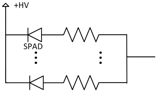
Figure 1. Schematic of an analog SiPM.
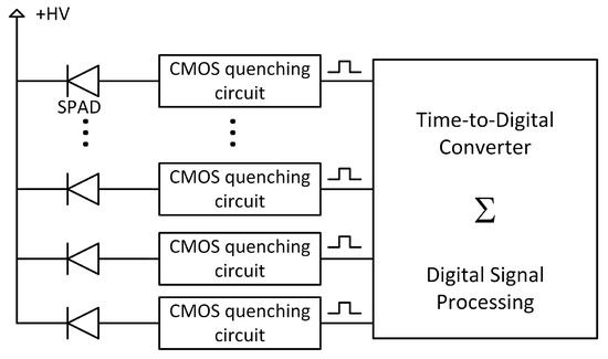
Figure 2. Schematic of a PDC. A CMOS microelectronic circuit is used to quench 1-to-1 a given SPAD.
Historical Review of SPAD-Based Photodetector
From 1950 to 1960, most SPAD research was on studying the micro-plasma that is created in a p-n junction and which is the foundation of the avalanche breakdown process [25,26,27,28]. In the following years, the term avalanche photodiode emerged [29] and, at the beginning of the 70s, the first avalanche photodiodes were commercially available from RCA [30]. In parallel, Cova and his team started working on SPADs and invented the quenching circuit (QC) to build a single-photon detector [31,32]. The first SPAD-based systems were implemented using discrete electronic components to form a single-channel SPAD detector [33]. Their performance in terms of noise, speed and timing measurement accuracy were limited by the large capacitance of a long interconnection (∼cm) between the discrete SPAD and the readout quenching circuit [34]. During the 80s and the 90s, the field progressed significantly in understanding the SPAD nuisance parameters and overall characteristics. In 1998, the MIT Lincoln Lab was the first to build a 4×4
SPAD array that was piggybacked on a 16-channel readout ASIC for a LiDAR application [18,20]. Still at that point, each SPAD was wirebonded to its readout channel. To lower the capacitance between the SPAD and its readout circuit, the next major step came when single-photon detectors took the avenue of microelectronics integration, with the goal to integrate both the SPAD and readout quenching circuit into a single commercial microelectronics process [35,36,37,38,39,40]. These innovations led into the early 2000s to the first multi-pixel SPAD arrays, grouped in this review under 2D PDCs [41,42]. 2D PDCs have progressed tremendously since then and the literature is abundant on the topic (see references in [43]). It is interesting and counterintuitive to note that the first analog SiPMs were presented by Saveliev and Golovin in 2000 [2] while a lot of work was already ongoing on the digital approach.
2. Analog versus Digital SPAD Array
In this section, analog SiPMs and PDCs are compared with highlights on their major differences.
2.1. Paradigm Shift or Back to the Start?
To read out an analog SiPM, one must use a charge sensitive preamplifier, a transimpedance amplifier or a current amplifier [44]. The signal is then shaped to obtain single-photon resolution with proper signal-to-noise ratio. Finally, the signal is digitized by an analog-to-digital converter. However, one must realize that the Boolean information about the state of each SPAD (triggered or not) was already available at the SPAD level. Therefore, analog SiPMs convert Boolean information into an analog signal that is then digitized again at the cost of power consumption and complex analog readout. On the contrary, in a PDC, each SPAD is read out individually by its own quenching circuit, acting like a leading-edge discriminator and outputting a binary signal corresponding to the SPAD state. At that point, proper digital signal processing can be implemented to meet the application goal.
2.2. Reading Out Each SPAD Individually
Reading out each SPAD individually in a PDC has significant advantages. Within a SPAD array, the breakdown voltage varies from SPAD to SPAD due to fabrication process deviations, temperature variation and IR drop that is a function of the position [45]. When performing single-photon counting with analog SiPMs, these fluctuations blur the spectrum at high photon counts. With a PDC, each triggered SPAD raises a flag processed by the digital logic [41,42,46,47,48]. Most variations in the SPAD’s response are thus masked by the digital conversion performed by the quenching circuit which therefore provides a greater SPAD-to-SPAD variation immunity. This can be exploited to achieve more accurate energy measurement, improved single-photon timing resolution (SPTR), better sensor uniformity, and lower sensitivity to temperature variation.
Both analog SiPMs and PDCs have the ability to measure single photons. In the readout chain of an analog SiPM, each stage including the analog-to-digital converter contributes to the noise of the measurement [49,50]. In a well-designed readout chain, the noise is dominated by the output capacitance of the SiPM. This can be mitigated by increasing the transconductance of the first transistor in the readout path with a large current, but at the cost of an increased power consumption [51].
With a PDC, the concept of electronic noise is irrelevant to the ability to resolve single photons. The signal-to-noise ratio of the readout chain does not scale with the capacitance of the SPAD, as opposed to analog SiPMs. A given quenching circuit sees the small capacitance of only one SPAD (~tens to hundreds of fF) and a fast-rising voltage step with an amplitude equal to the difference between the SPAD bias voltage and its breakdown voltage (known as Vexcess). The quenching circuit acts as a leading-edge discriminator providing single-photon resolution.
SPADs may be damaged during fabrication, exhibit a noise count rate above specification, or get radiation damage within the experiment [52]. In an array, resolving single photons may therefore become impossible as the noise floor, i.e., the average number of triggered SPADs without excitation, increases. In extreme cases, an analog SiPM might need to be shut down with the consequence of losing photosensitive area equal to the SiPM size. Regarding radiation damage specifically, SiPMs’ radiation hardness is increased by decreasing the SPAD size at the cost of fill-factor. In the case of PDCs, noisy SPADs can be turned off or their bias voltage can be adjusted through the integrated circuit programming interface [53]. This way, the noise floor does not increase, preserving single-photon resolution, while the total dynamic range is lowered only by the number of disabled SPADs.
The photon detection efficiency (PDE) of a SPAD is proportional to its quantum efficiency at a given wavelength and to the probability of triggering a sustainable avalanche as a function of the excess voltage. With an analog SiPM, there is no control on the recharge time resulting in an effective dynamic PDE change while recharging the SPAD. With a PDC, one can swiftly recharge the SPAD with a CMOS circuit, providing greater PDE uniformity and single-photon counting.
Optical crosstalk and afterpulsing are correlated noises which pollute the signal in all types of SPAD-based detector. They are proportional to the number of charges involved in the avalanche of a SPAD [54]. Analog SiPMs have no control over the quenching and recharge of each SPAD during operation. On the contrary with PDCs, an avalanche can be detected at its beginning and be swiftly quenched, thus limiting the charges involved in the avalanche. To limit afterpulsing noise, a programmable delay can be implemented in a PDC, to keep each SPAD off over a desired period of time after it was triggered. This allows for the trapped charges to be released without triggering a new avalanche, which improves the effective PDE [55]. By programming the hold-off time and the recharge time, the correlated noise can be significantly reduced during operation, at the cost of a detection deadtime. This is a major advantage of PDCs over analog SiPMs.
2.3. Power Consumption Comparison
It is a complex task to compare the power consumption of systems that do not have the same approach, in particular, when the output information is in a different form. For photon counting with an analog solution, the first stage of amplification (current, transconductance or charge sensitive amplifiers), shaper, sample and hold and ADC are continuously consuming power, whether there are events or not. With PDCs based on CMOS readout circuits, the absence of events leads to very low power consumption in the quenching circuit while the digital counter logic consumption is only significant when a SPAD is triggered. The idle power consumption is set by auxiliary circuits (ex: monostable and bias circuits—depending on the integrated circuit architecture) and the transistor gate leakage current, which can be non-negligible for large-scale detectors and deep sub-micron technologies [56]. Moreover, PDCs can work synchronously with a constant clock or asynchronously where the clock is only activated when data is available. The latter option leads to a significant reduction in power consumption.
3. 2D versus 3D Integrated PDC
A 2D PDC consists of an array of SPADs and quenching circuits integrated together in a CMOS process [41,42,46,47,57,58]. The SPAD is usually a shallow planar junction implemented using the transistor drain/source implantation in a well of the opposite type as shown in Figure 3. Please note that the dopant type could be inverted (n+ into p-type well), as long as options are available for the guard ring. The guard ring’s purpose is to prevent undesired lateral breakdown [59,60].
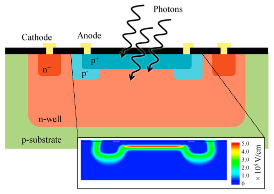
Figure 3. Cross-section of a CMOS SPAD. Shown here is a frontside illuminated p+ in n-well SPAD. The inset shows a uniform high electric field region under the whole sensitive area of the SPAD achieved by optimization of the guard-ring geometry and doping level.
The parameters set by the foundry (implantation level, atom/molecule used to dope, etc.) are serious limitations to design state-of-the-art SPADs [61]. Some groups overcame this limitation either by applying a CMOS compatible process modification (through a direct partnership with the foundry) [62] or by using a high-voltage or imaging CMOS technology [62,63]. In all cases, trade-offs must occur because the SPAD and electronics share the same technology node.
Some 2D PDCs have large area SPADs, but limited electronic functionalities within the SPAD-QC pixel (Figure 4a) to increase the photosensitive fill-factor [57]. Others have smaller SPADs, but with more in-pixel electronic functionalities (Figure 4b) such as a counter, a time-to-digital converter (TDC), programmable hold-off time, masking of noisy SPAD, etc. [64,65]. This trade-off between photosensitive area and functionalities is inherent to the 2D architecture. In radiation instrumentation, a high fill-factor is preferred when there are very few photons or when the detection of an event’s first photons is desired [43,57]. This brings an important comment on the fill-factor: it is essential to state for a given system if the reported fill-factor includes the peripheral electronic circuits (counter, TDC, bias for monostable circuits, etc.) or if the fill-factor is provided only for the SPAD array. Each of these definitions can be a sound performance parameter depending on the application under consideration. For example, the chip level fill-factor (i.e., peripheral electronics, pads surrounding the array, space for wirebonding) must be considered for photon loss when the application requires large area detectors. This is the case for large-scale, low-background physics experiments, where large detector tiles are implemented [12,15,66].
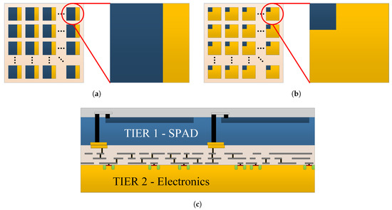
Figure 4. Illustration of the trade-off between the SPAD and the electronic functionality for 2D PDCs sharing the same technology node compared to a 3D PDC. In (a), a 2D PDC with large SPAD (blue), but limited in-pixel electronics functionalities (yellow). In (b), a 2D PDC with small SPAD (blue), but greater in-pixel electronic functionalities (yellow). In (c), a 3D PDC with large SPAD (blue) and large area for in-pixel electronic functionality (yellow).
Designing 2D PDCs in CMOS benefits from using already available technologies. It allows for rapid prototyping, avoids development cost, ensures industrial yield and reliability and provides well-established electronics design kits. Furthermore, the close integration of the SPAD-QC pair allows the reading node capacitance to be as low as possible. This reduces the charge per avalanche and thus the correlated noise (afterpulsing and crosstalk) [67]. This makes the 2D PDC an excellent option in applications where the fill-factor is less of a concern (i.e., high photon flux), such as in LiDAR sensors [68]. One of the drawbacks is related to the technology choice: with both SPAD and electronics sharing the same fabrication process, one cannot independently choose the optimal process for the SPAD (imaging CMOS, custom process, high-voltage CMOS, etc.) and the optimal process for the electronics (deep sub-micron CMOS, fast CMOS, low power CMOS, etc.).
In light of the above, there is a trend toward developing 3D heterogenous vertical integration of a SPAD array over a CMOS chip. This avoids the 2D PDC trade-offs and thus enables to reach the ultimate single-photon detector. Figure 4c is an illustration of such a 3D integrated PDC [59]. In this scheme, a high fill-factor front side illuminated SPAD array is implemented on the first tier (dedicated SPAD process). The underneath electronics (second tier) is implemented in a chosen CMOS process according to the levels of complexity and functionality needed by the application [46,48,69,70,71,72].
This entry is adapted from the peer-reviewed paper 10.3390/s21020598