Herein, the surface properties of gallium nitride (GaN) of the wurtzite form, (0001) oriented are presented. X-ray and UV photoelectron spectroscopies (XPS, UPS) were employed to show chemical and physical characters of the surface . Basic information about electronic structure of various doped GaN(0001) surfaces as well as surface Fermi level pinning are discussed.
- GaN(0001)
- thin films
- photoelectron spectroscopy
- surface science
1. Introduction
A current challenge of modern science is developing more perfect light sources and electronic components able to work at high frequency and power. A very good base material for realization of the above mentioned goals is gallium nitride (GaN) belonging to the family of group III-V semiconductors. It can occur in the zinc blende or wurtzite structure, its latter form in particular is very attractive from the technological point of view due to the physical properties, i.e. wide and direct band gap, relatively high mobility of carriers, and high breakdown voltage. These properties predispose GaN as a substrate for modern electronic devices production [1,2]. The use of gallium nitride in the semiconductor industry is a merit of intense research carried out for over 30 years. As a breakthrough moment of the development of research topics related to GaN should be considered the mastering of the technique of doping this semiconductor, in particular to the p-type [3–5]. These discoveries have directly contributed to the possibility of producing electronic devices, including diodes emitting blue light [6–8], for the production of which Akasaki, Amano, and Nakamura were awarded the Nobel Prize in 2014 [9]. Gallium nitride in the wurtzite form, (0001)-face oriented, universally used in basic research, as well as in industry, is mainly grown on sapphire substrates by metalorganic vapour phase epitaxy (MVPE) [10] and molecular beam epitaxy (MBE) [11]. Well mastered techniques of growth enable production of semiconductor structures with desired electronic parameters through creating GaN-based alloys with other elements. This gives a large possibility of producing diverse electronic devices based on thin-film multistructures. The properties of such structures are largely determined at the interface, and thus depend on the features of the initial surface, i.e. GaN(0001). Therefore, knowledge of properties of bare GaN surfaces is necessary to understand the mechanisms of operation of more advanced systems [12].
In order to interpret photoelectron studies, it is necessary to understand the differences in the electronic structure of bare n-, p-, and non-doped GaN (0001) surfaces. Despite the wide availability of professional literature on these topics and very good and extensive reviews [12,13], there are still papers containing misinterpretations of the basic results obtained in photoemission experiments. Herein, the basic information about GN(0001) surfaces obtained in photoelectron experiments are presented.
2. GaN(0001) Surface
The GaN material contains gallium and nitrogen atoms in 1:1 stoichiometry, forming the hexagonal N-Ga diatomic layer in which the atoms are arranged in imperfect tetrahedral geometry due to different atom sizes and the electronegativity of Ga and N atoms. The hexagonal N-Ga diatomic layers, forming an hcp structure, can be stacked on top of each other in the c-direction, taking places A, B, or C, as shown in Figure 1. There are two stable GaN structures with the ABAB . or ABCABC . stacking sequences, for which GaN crystals are obtained in the form of the wurtzite- or zinc-blend, respectively. In addition to being different in structure, both materials have other electronic properties [14–16]. GaN(0001) has the wurtzite form and is terminated with Ga atoms, unlike the (000) surface, on top of which N atoms are situated.
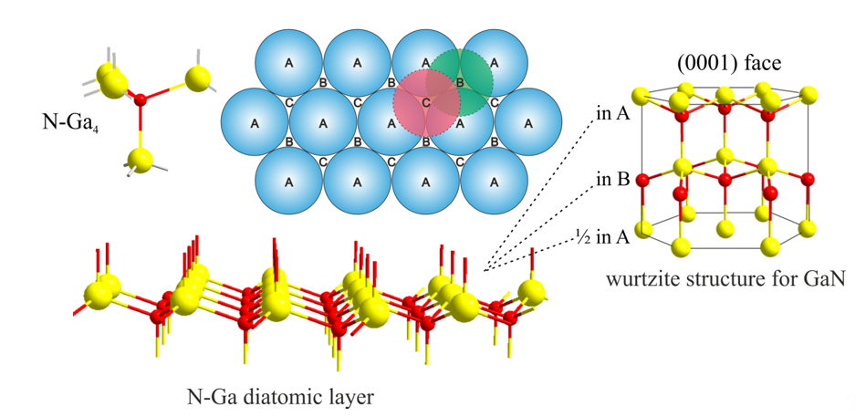
Figure 1. Structure of gallium nitride (GaN): particle of Ga4N in tetrahedral geometry, N-Ga diatomic hexagonal sheet, hexagonal close-packing (hcp) position model, and hcp structure with ABAB-type layering.
Below are the results of the non-doped (0001)-oriented GaN sample, precleaned with isopropanol, then cleaned in situ using short-time annealing under UHV conditions at a temperature of about 800 °C. The broad XPS spectra of the sample, obtained with 1253.6 and 1486.7 eV photons, are shown in Figure 1. Besides the Ga-2p, Ga-3s, Ga-3p, N-1s peaks from GaN, the C-1s, O-1s core-level lines that are derived from carbon and oxygen impurities are also visible. Auger electrons emitted from a sample exposed to X-rays also contribute to the collected spectra. They form characteristic energy levels from Auger transitions in atoms presented on surfaces and subsurface layers. In Figure 2, there are many electrons from Ga LLM transitions, especially two intensive levels, i.e., L3M45M45 and L2M45M45, with kinetic energies of about 1065 and 1091 eV, respectively. It is also worth noting that the kinetic energy of Auger electrons does not depend on the energy of excitation radiation (unlike photoelectrons). Thus, the same Auger levels in spectra obtained with different photon energies are located at different spots of the BE, as shown in Figure 2. Furthermore, in the case of measurements with the Mg Kα excitation line, carbon content on GaN surfaces cannot be determined because the C-1s line is covered by one of the Ga LMM levels. For experiments with Al Kα photons, the N-1s line partly overlaps with the Auger signal.
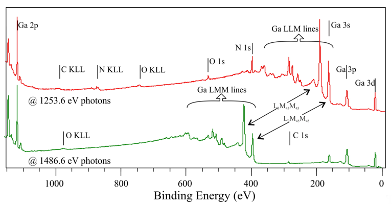
Figure 2. Survey spectra for a nondoped GaN(0001) surface, collected with different photon energies.
The influence of standard commonly used radiation sources on the obtained spectra shape is shown in Figure 3. On the GaN(0001) surface, where a trace amount of oxygen is present, the Ga-3d shallow core-level line with a BE of 20.4 V contains four subpeaks. The main one is from the Ga–N bonds, while the other two correspond to Ga–O and Ga–Ga bonds and the last one comes from the overlap N-2s state [17–20]. The X-ray source type has little effect on the shape of the Ga-3d peaks obtained, but this is not the case for the valence band (VB), where the impact is significant, as shown in Figure 3a. This is due to the overlap of the X-ray satellite of the Ga-3d peak on the VB, measured with nonmonochromatic sources, and the different depths from which the electrons originate. The kinetic energy of ejected electrons from the VB, excited with 1253.6 eV (Mg Kα) and 1486.7 eV (Al Kα) photons, varies significantly, causing them to have different inelastic mean free paths. This results in signals collected with different photon sources coming from various sample depths.
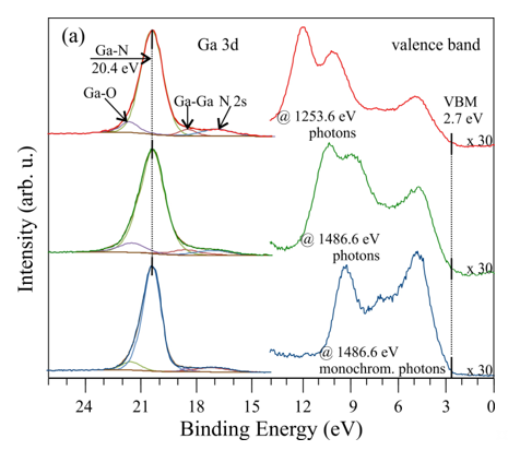
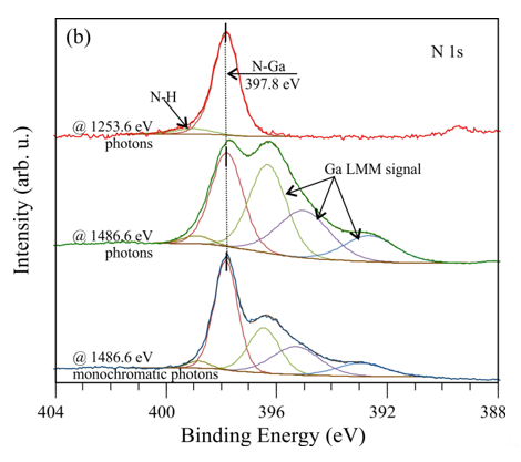
Figure 3. X-ray photoelectron spectroscopy (XPS) spectra of (a) Ga-3d and the valence band as well as (b) the N 1s for a nondoped GaN(0001) surface, collected with different photon sources.
Despite different shapes, the valence band maximum (VBM) is located 2.7 eV below the EF and is found from a linear extrapolation of the leading edge of the spectrum to the background. In Figure 3b, the N-1s spectrum collected with Mg Kα photons consists of two elements: one is assigned to the N–Ga bonding with the BE of 397.8 eV and the other to N–H bonds. This spectrum, obtained with the Al Kα excitation line, has five subpeaks: similarly, the first two peaks correspond to the N–Ga and N–H bonds, and the other comes from the Ga LMM. The Auger signal is suppressed for measurements with a monochromator. The energy difference between the N-1s and Ga-3d peaks is eV and is consistent with other literature for GaN [21].
Cleaning the surface of GaN crystals under UHV is problematic because it can lead to changes in the surface stoichiometry, regardless of whether it is an ion bombardment or annealing. Ion bombardments may introduce defects and preferentially remove nitrogen atoms [22–24]. To eliminate this effect, the post-bombardment annealing method or low-energy N-ion bombardment can be utilized [25,26]. The most convenient and simplest technique of surface preparation in UHV is annealing. However, during this process, the surface may also be decomposed [27]. Thus, rapid thermal annealing (RTA) should be applied. The effect of carbon and oxygen contaminant elimination by this method is shown in Figure 4. One can see that annealing in UHV may eliminate surface contamination. Two annealing cycles at 800 °C significantly reduces the signal from C and O contaminants (green lines), and six cycles lead to the achievement of a carbon- and oxygen-free GaN(0001) surface (blue lines). Unfortunately, sometimes, this method does not cause a complete elimination of contaminants, of which XPS signals remain as the middle curves in Figure 4. This is most likely dependent on the results of precleaning the sample surface by chemical treatment prior to placing it in UHV systems.
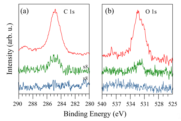
Figure 4. XPS spectrum intensity of (a) C-1s and (b) O-1s for a nondoped GaN(0001) surface. Upper spectrum corresponds to the degassed surfaces in UHV; lower ones show the influence of different numbers of annealing cycles at 800 °C.
RTA can also guarantee a high-quality surface, as confirmed by LEED patterns in Figure 5a, where the strong intensity and sharp spots of GaN(0001)-(1 × 1) are visible. Several cycles of RTA may rebuild the surface, forming a facet-like terrace structure by changing the diffraction pattern [28,29]. As a result of such rebuilding, the sextets of diffraction spots appear in a hexagonal configuration around each main spot (see Figure 5b). The energy positions of the core-level line measured by XPS may vary significantly depending on the type and concentration of the dopant used in GaN. Those peak shifts do not necessarily result from the chemical properties of the surface but may only arise from different locations of the Fermi level in n-, p-, and non-doped GaN. In the perfect non-doped GaN, the EF in bulk material falls more or less in the middle of the forbidden gap; in the n-type, it is located close to the conduction band minimum, and, in the p-type, it is placed near the valance band maximum. Since photoemissions are surface-sensitive techniques, the EF position on the surface of the tested material is crucial. Due to the surface density of states (SDOSs) present on the GaN(0001), the surface Fermi level is located in a different position than in bulk material [30–33]. This means that the energy bands at the surface are bent upwards or downwards, depending on the dopant type. Figure 6 shows the distance between the valence band maximum and the surface Fermi level for Si- (n-), Mg- (p-), and non-doped GaN.
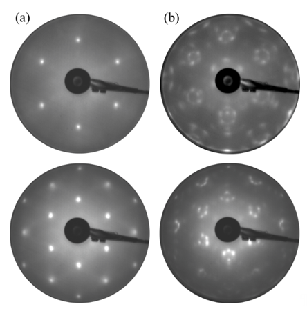
Figure 5. Low-energy electron diffraction (LEED) patterns for the GaN(0001)-(1 × 1) structure. Image (a) is attributed to flat well-ordered surfaces; (b) shows the presence of facets. Images were taken with an electron beam of 90 (upper) and 155 eV (bottom).
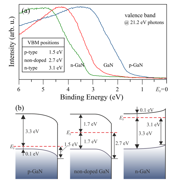
Figure 6. (a) Ultraviolet photoelectron spectroscopy (UPS) spectra of the valence band for n-, p-, and nondoped GaN(0001). (b) Energy band diagram visualization of (a). The Fermi level positions in bulk materials were determined for n- and p-type GaN, respectively.
Furthermore, it indicates the difference in the EF location on the surface and in bulk. Moreover, SPV appears on GaN during XPS and UPS measurements, which results in band-bending changes [21,30]. Thus, the surface EF position relative to the VBM may also vary, depending on the magnitude of the SPV. This effect is presented below in the example of a GaN surface that is covered with native oxide and not subjected to any preparation [30]. The appointed positions of the valence band maximum of the measurements with a Kelvin probe (working in air) were compared with the VBM positions in the XPS results. Schemes of energy bands for the n-type GaN(0001) surface, in the dark (without SPV) and illuminated with UV light, were obtained, as shown in Figure 7.
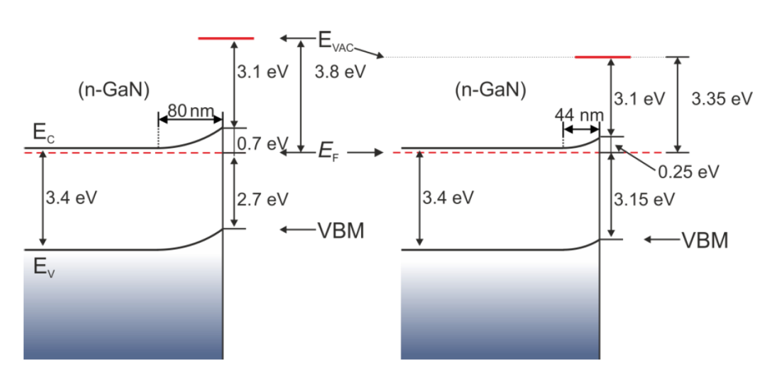
Figure 7. Energy band diagram for n-GaN(0001) in the dark (left) and illuminated with UV photons (right). Reprinted with permission from [30]. Copyright 2020 Elsevier.
On the sample in the dark, the Fermi level was located 2.7 eV above the VBM. It is a value corresponding to the higher surface density of states calculated by Segev and Van de Walle [31,32] and the position measured by Janicki and coauthors [33] for a structure with n-type doping. This value is slightly larger than the one determined by Long and Bermudez [21]. After illumination, it comes to a flattening of bands; surface photovoltage is 0.45 V. It leads to the EF location change, relative to the VBM from 2.7 to 3.15 eV. The measurement of the valence band and the Ga-3d shallow core level for the same sample is shown in Figure 8.
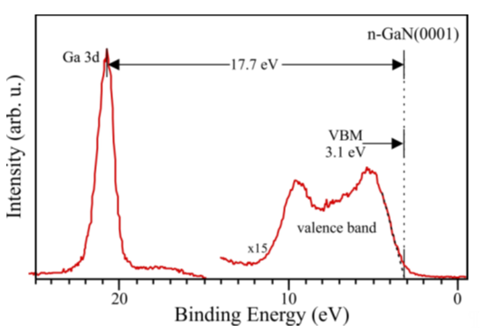
Figure 8. XPS measurement of an n-GaN(0001) sample. Visible Ga-3d electron state and valence band. Reprinted with permission from [30]. Copyright 2020 Elsevier.
As can be seen above, the VBM position relative to the Fermi level falling to zero is 3.1 eV. The value is in line with the one obtained in the measurements with a Kelvin probe for the illuminated sample. The outcomes for p-GaN(0001) covered with native oxide also showed that the EF level for the sample in the dark is located 1.75 eV above the valence band maximum and corresponds to lower SDOS, as calculated by Segev and Van de Walle, and the value measured by Janicki for a sample with p-type doping. After illuminating the p-GaN(0001) surface with UV photons, the energetic bands flatten and the EF level locates 1.2 eV above the VBM. The same value was obtained with XPS measurements; therefore, when the surface is irradiated with X-rays, the SVP voltage is the same as the one obtained with UV light illumination (−0.55 V) [30].
The results presented in [30,33] show the bistability of the Fermi level. It should be noted that although the energies of the Fermi levels measured on the surface are practically the same as in the theoretical calculations [31,32], the nature of SDOS found experimentally differs from the calculated one. The existence of lower SDOS in the calculations is related to the (2 × 2)-GaT4 reconstruction—such reconstruction would not survive on an oxidized surface or on non-doped GaN/doped GaN samples used in Janicki’s work phase boundaries [33].
As mentioned before, surface preparation is a very important stage in the process of formation of an electronic device. Cleaning through bombardment, which is usually carried out using high energy (1–10 or even 10–500 keV), can cause large changes in the structure morphology. Therefore, in order to counteract the changes in GaN surface properties and its degradation, less-invasive cleaning processes are needed. In [25,26], a process of bombardment with nitrogen ions, with a relatively low energy level of 200 eV, was proposed. This solution enables the cleaning of the surface by sputtering, yet is much less destructive and also compensates for nitrogen loss from the near-surface region. During the bombardment, the nitrogen is partly implanted. The study shows the impact of N-ion bombardment of the n-GaN(0001) surface on its physicochemical changes [25]. As a result of the surface bombardment, there is a change in the UPS spectrum, as shown in Figure 9.
.
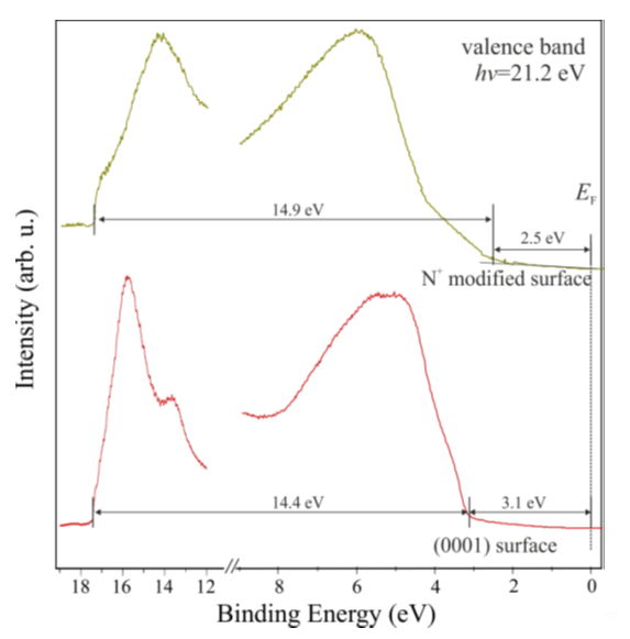
Figure 9. UPS spectrum for n-GaN(0001) before and after bombardment with N ions. Reprinted with permission from [25]. Copyright Acta Phys. Pol. A.
After bombardment, the valence band maximum shifts towards lower binding energies, from 3.1 to 2.5 eV. The same happens with the Ga-3d and N-1s core level lines; they also shift towards lower binding energies. The influence of bombardment on the electronic structure is schematically presented in Figure 10. Despite the process of bombardment being effectuated at relatively low energy, the receiving GaN surface is not orderly—there are no diffraction images.
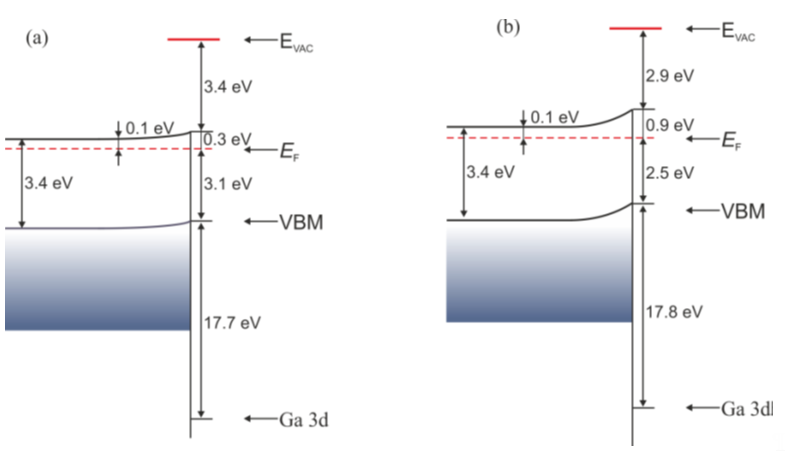
Figure 10. Energy band diagram for n-GaN(0001) (a) before and (b) after bombardment with N ions. Reprinted with permission from [25]. Copyright Acta Phys. Pol. A.
In the case of a p-type surface, bombardment with N ions also leads to changes [26]. However, in this case, the bands bend even more. The EF level is in the same position as on the bombarded n-GaN surface, i.e., 2.5 eV above the VBM. The Ga-3d and N-1s core level lines behave similarly. It can be reasoned that as an effect of bombardment, there is an inversion of carrier occupation in the subsurface layer, and the surface shows an n-type feature. Interestingly, after a short annealing of a bombarded p-GaN surface, there is a splitting of the Ga-3d and N-1s peaks. Two curves are also observed in the valence band spectrum—its top edge has two slopes. The results are shown in Figure 11. The components A, B, which are included in the Ga-3d spectrum, are located around 17.7 eV below the two edges of the valence band, which are separated by 1.5 eV. The same value separates the components included in the N-1s line. This suggests the emergence of two regions on the surface that are electrically separated—one with n-type properties, the other with p-type properties.
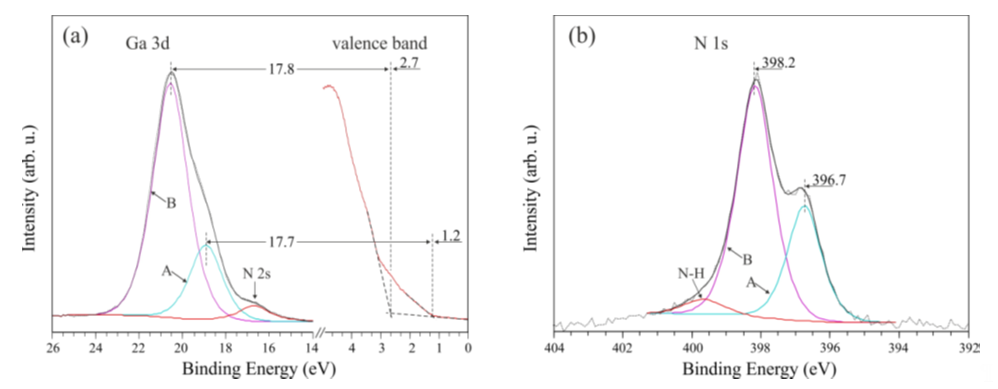
Figure 11. XPS measurement of a p-GaN(0001) sample. (a) Ga-3d electronic state and valence band; (b) N-1s core level. Reprinted with permission from [26]. Copyright 2018 Elsevier.
It is worth noting that bombardment with nitrogen ions leads to changes in the band bending of both the n-GaN and p-GaN samples; the Fermi level is located 2.5 eV above the VBM, which is in line with the result obtained by Long and Bermudez [21]. Such a result may be an effect of a decrease in the influence of the SPV voltage on both surfaces, as well as the introduction of donor states on the p-GaN surface, causing the EF pinning at higher SDOS, deriving from gallium dangling bonds.
Therefore, the dispersion in Fermi level placement in relation to the valence band maximum in photoemission experiments, which is also observed in the author’s publications, can be caused by a different condition of the GaN surface—different concentrations of donor and acceptor states on the surface, in subsurface layers, and in the bulk samples used. Moreover, surface quality and the number of defects can also have an influence on the magnitude of surface photovoltage. To determine whether the peak shift is caused by a chemical reaction or not, its location relative to the VMB needs to be known. As shown above, on the GaN(0001) surface, the Ga-3d state is located around 17.7 eV above the VBM. There are also different values of the ∆E in the literature, with a spread of ±0.3 eV from the value indicated here.
The properties of the surfaces can be modified by presence of adatoms on it. Thus, the presence of about 1 monolayer of As atoms leads to the formation of a surface state [34]. Sb adatoms modify the electronic properties of the surface, change the position of the maximum of the valence band, lower the levels of electronic affinity [35]. The latter is especially affected by the presence of cesium atoms, which can even lead to negative electron affinity [36–38].
3. Conclusion
Photoelectron spectroscopies (XPS, UPS) were used to investigate properties of GaN(0001) surfaces. GaN(0001) was characterized with different X-ray excitation sources, i.e., nonmonochromatic Mg Kα (1253.6 eV) and non- and monochromatic Al Kα (1486.6 eV). Their influence on the shapes of the core level lines and the valence band were found. The type of X-ray source has a particularly large impact on the shape of the N-1s line due to the overlap of the Auger lines that occur for photons with an energy of 1487.6 eV. Significant changes were also observed in the valence band, caused by overlapping with X-ray satellites in the case of nonmonochromatic sources. The binding energy positions of Auger lines vs. X-ray sources are shown. Electronic properties of non- and various doped GaN(0001) surfaces studied by UPS are presented. The valence band maxima lie 2.7 eV below the Fermi level for nondoped GaN and, in the case of doped materials, they are at 3.1 and 1.5 eV for the n- and p-type semiconductors, respectively. The bistability of the Fermi level was demonstrated. The research has also shown the influence of surface photovoltage on the band bending. Moreover the influence of bombardment with N ions on GaN(0001) surface properties was determined. It was observed that on GaN surfaces after bombardment the Fermi level is located at the same place regardless whether the sample was doped to n- or p-type.
References
-
- Lidow, J. Strydom, M. de Rooij, D. Reusch, eds., GaN Technology Overview, in: GaN Transistors for Efficient Power Conversion, John Wiley & Sons Ltd, 2014: pp. 1–18. https://doi.org/10.1002/9781118844779.ch01.
- Mochizuki, Vertical GaN and SiC Power Devices, Artech House, 2018.
- Amano, M. Kito, K. Hiramatsu, I. Akasaki, P-Type Conduction in Mg-Doped GaN Treated with Low-Energy Electron Beam Irradiation (LEEBI), Jpn. J. Appl. Phys. 28 (1989) L2112. https://doi.org/10.1143/JJAP.28.L2112.
- Nakamura, M. Senoh, T. Mukai, Highly P-Typed Mg-Doped GaN Films Grown with GaN Buffer Layers, Jpn. J. Appl. Phys. 30 (1991) L1708. https://doi.org/10.1143/JJAP.30.L1708.
- Nakamura, T. Mukai, M. Senoh, N. Iwasa, Thermal Annealing Effects on P-Type Mg-Doped GaN Films, Jpn. J. Appl. Phys. 31 (1992) L139. https://doi.org/10.1143/JJAP.31.L139.
- Nakamura, T. Mukai, High-Quality InGaN Films Grown on GaN Films, Jpn. J. Appl. Phys. 31 (1992) L1457. https://doi.org/10.1143/JJAP.31.L1457.
- Murakami, T. Asahi, H. Amano, K. Hiramatsu, N. Sawaki, I. Akasaki, Growth of Si-doped AlxGa1–xN on (0001) sapphire substrate by metalorganic vapor phase epitaxy, Journal of Crystal Growth. 115 (1991) 648–651. https://doi.org/10.1016/0022-0248(91)90820-U.
- Akasaki, H. Amano, H. Murakami, M. Sassa, H. Kato, K. Manabe, Growth of GaN and AlGaN for UV/blue p-n junction diodes, Journal of Crystal Growth. 128 (1993) 379–383. https://doi.org/10.1016/0022-0248(93)90352-W.
- The Nobel Prize in Physics 2014, NobelPrize.Org. https://www.nobelprize.org/prizes/physics/2014/summary/ (accessed October 8, 2020).
- Amano, N. Sawaki, I. Akasaki, Y. Toyoda, Metalorganic vapor phase epitaxial growth of a high quality GaN film using an AlN buffer layer, Appl. Phys. Lett. 48 (1986) 353–355. https://doi.org/10.1063/1.96549.
- [11] Wang, A. Yoshikawa, Molecular beam epitaxy growth of GaN, AlN and InN, Progress in Crystal Growth and Characterization of Materials. 48–49 (2004) 42–103. https://doi.org/10.1016/j.pcrysgrow.2005.03.002.
- M. Bermudez, The fundamental surface science of wurtzite gallium nitride, Surface Science Reports. 72 (2017) 147–315. https://doi.org/10.1016/j.surfrep.2017.05.001.
- M. Feenstra, J.E. Northrup, J. Neugebauer, Review of Structure of Bare and Adsorbate-Covered GaN(0001) Surfaces, Materials Research Society Internet Journal of Nitride Semiconductor Research. 7 (2002). https://doi.org/10.1557/S1092578300000296.
- Pugh, D. Dugdale, S. Brand, R. Abram, Electronic Structure Calculations on Nitride Semiconductors, Semiconductor Science and Technology. 14 (1999) 23. https://doi.org/10.1088/0268-1242/14/1/003.
- Madelung, Semiconductors: Data Handbook, Springer Science & Business Media, 2004.
- Michael E. Levinshtein , Sergey L. Rumyantsev , Michael S. Shur, Properties of Advanced Semiconductor Materials: GaN, AIN, InN, BN, SiC, SiGe | Wiley, 2001. https://www.wiley.com/en-us/Properties+of+Advanced+Semiconductor+Materials%3A+GaN%2C+AIN%2C+InN%2C+BN%2C+SiC%2C+SiGe-p-9780471358275 (accessed April 28, 2020).
- Grodzicki, P. Mazur, A. Krupski, A. Ciszewski, Studies of early stages of Mn/GaN(0001) interface formation using surface-sensitive techniques, Vacuum. 153 (2018) 12–16. https://doi.org/10.1016/j.vacuum.2018.03.059.
- Grodzicki, J.-G. Rousset, P. Ciechanowicz, E. Piskorska-Hommel, D. Hommel, XPS studies on the role of arsenic incorporated into GaN, Vacuum. 167 (2019) 73–76. https://doi.org/10.1016/j.vacuum.2019.05.043.
- Grodzicki, P. Mazur, S. Zuber, J. Brona, A. Ciszewski, Oxidation of GaN(0001) by low-energy ion bombardment, Applied Surface Science. 304 (2014) 20–23. https://doi.org/10.1016/j.apsusc.2013.11.146.
- Falta, Th. Schmidt, S. Gangopadhyay, Chr. Schulz, S. Kuhr, N. Berner, J.I. Flege, A. Pretorius, A. Rosenauer, K. Sebald, H. Lohmeyer, J. Gutowski, S. Figge, T. Yamaguchi, D. Hommel, Cleaning and growth morphology of GaN and InGaN surfaces, Phys. Status Solidi B. 248 (2011) 1800–1809. https://doi.org/10.1002/pssb.201046574.
- P. Long, V.M. Bermudez, Band bending and photoemission-induced surface photovoltages on clean n- and p-GaN (0001) surfaces, Phys. Rev. B. 66 (2002) 121308. https://doi.org/10.1103/PhysRevB.66.121308.
- Majchrzak, M. Grodzicki, P. Ciechanowicz, J.-G. Rousset, E. Piskorska-Hommel, D. Hommel, The influence of oxygen and carbon contaminants on the valence band of p-GaN(0001), Acta Physica Polonica A. (2019).
- Kovač, A. Zalar, Surface composition changes in GaN induced by argon ion bombardment, Surface and Interface Analysis. 34 (2002) 253–256. https://doi.org/10.1002/sia.1294.
- Despiau-Pujo, P. Chabert, MD simulations of GaN sputtering by Ar+ ions: Ion-induced damage and near-surface modification under continuous bombardment, Journal of Vacuum Science & Technology A. 28 (2010) 1105–1110. https://doi.org/10.1116/1.3460904.
- Grodzicki, P. Mazur, A. Ciszewski, Modification of Electronic Structure of n-GaN(0001) Surface by N+-Ion Bombardment, Acta Physica Polonica A. 132 (2017) 351–353. https://doi.org/10.12693/APhysPolA.131.351.
- Grodzicki, P. Mazur, A. Ciszewski, Changes of electronic properties of p-GaN(0 0 0 1) surface after low-energy N+-ion bombardment, Applied Surface Science. 440 (2018) 547–552. https://doi.org/10.1016/j.apsusc.2018.01.097.
- D. Koleske, A.E. Wickenden, R.L. Henry, W.J. DeSisto, R.J. Gorman, Growth model for GaN with comparison to structural, optical, and electrical properties, Journal of Applied Physics. 84 (1998) 1998–2010. https://doi.org/10.1063/1.368353.
- Janzen, C. Hahn, T.U. Kampen, W. Mönch, Explanation of multiplet spots in low-energy electron diffraction patterns of clean GaN surfaces, Eur. Phys. J. B. 7 (1999) 1–4. https://doi.org/10.1007/s100510050583.
- S. Tautz, S. Sloboshanin, U. Starke, J.A. Schaefer, Reactivity and morphology of (10-1-2)-faceted and (3×3)-reconstructed GaN(000-1) epilayers grown on sapphire (0001), J. Phys.: Condens. Matter. 11 (1999) 8035–8048. https://doi.org/10.1088/0953-8984/11/41/307.
- Grodzicki, K. Moszak, D. Hommel, G.R. Bell, Bistable Fermi level pinning and surface photovoltage in GaN, Applied Surface Science. 533 (2020) 147416. https://doi.org/10.1016/j.apsusc.2020.147416.
- Segev, C.G.V. de Walle, Origins of Fermi-level pinning on GaN and InN polar and nonpolar surfaces, EPL. 76 (2006) 305. https://doi.org/10.1209/epl/i2006-10250-2.
- G. Van de Walle, D. Segev, Microscopic origins of surface states on nitride surfaces, Journal of Applied Physics. 101 (2007) 081704. https://doi.org/10.1063/1.2722731.
- Ł. Janicki, M. Gładysiewicz, J. Misiewicz, K. Klosek, M. Sobanska, P. Kempisty, Z.R. Zytkiewicz, R. Kudrawiec, Contactless electroreflectance studies of the Fermi level position at the air/GaN interface: Bistable nature of the Ga-polar surface, Applied Surface Science. 396 (2017) 1657–1666. https://doi.org/10.1016/j.apsusc.2016.12.013.
- Grodzicki, J.-G. Rousset, P. Ciechanowicz, E. Piskorska-Hommel, D. Hommel, Surface studies of physicochemical properties of As films on GaN(0001), Applied Surface Science. 493 (2019) 384–388. https://doi.org/10.1016/j.apsusc.2019.07.006.
- Grodzicki, P. Mazur, J. Pers, S. Zuber, A. Ciszewski, Sb Layers on p-GaN: UPS, XPS and LEED Study, Acta Physica Polonica A. 126 (2014) 1128–1130. https://doi.org/10.12693/APhysPolA.126.1128.
- Eyckeler, W. Mönch, T.U. Kampen, R. Dimitrov, O. Ambacher, M. Stutzmann, Negative electron affinity of cesiated p-GaN(0001) surfaces, Journal of Vacuum Science & Technology B: Microelectronics and Nanometer Structures Processing, Measurement, and Phenomena. 16 (1998) 2224–2228. https://doi.org/10.1116/1.590152.
- I. Wu, A. Kahn, Electronic states and effective negative electron affinity at cesiated p-GaN surfaces, Journal of Applied Physics. 86 (1999) 3209–3212. https://doi.org/10.1063/1.371191.
- I. Wu, A. Kahn, Negative electron affinity and electron emission at cesiated GaN and AlN surfaces, Applied Surface Science. 162–163 (2000) 250–255. https://doi.org/10.1016/S0169-4332(00)00200-2.
This entry is adapted from the peer-reviewed paper 10.3390/coatings11020145