A fundamental understanding of the growth of semiconductors is essential for the optimization of quantum dot-based optoelectronic devices. Droplet epitaxy has proven to be the successful versatile growth method for instance growing quantum dots with a small fine structure splitting for quantum information technology. Precise control and tuning of the quantum dots for various applications is only possible through a detailed understanding of the growth mechanism at the atomic level, which creates the need for atomic-scale structural and composition characterization. We present an overview of the results of detailed structural and composition analysis by cross-sectional scanning tunneling microscopy and atom probe tomography of quantum dots grown by self-assembled droplet epitaxy where we focus mainly on strain-free GaAs/AlGaAs and strained InAs/InP QDs.
- Quantum Dots
- Cross-sectional Scanning Tunneling Microscopy
- Atom Probe Tomography
- Droplet Epitaxy
- Optoelectronic Materials
- GaAs/AlGaAs QDs
- InAs/InP QDs
1. Introduction
Typical III-V semiconductor QDs are grown either by conventional molecular beam epitaxy (MBE) or metal-organic vapor phase epitaxy (MOVPE). In the early 1990s, mainly two growth mechanisms were proposed for the fabrication of self-assembled QDs: (i) Stranski-Krastanov growth mode and (ii) droplet epitaxy. Both growth modes are still being explored to further optimize the nanostructures for various novel applications.
2. Growth Mechanisms and Characterization Techniques of QDs
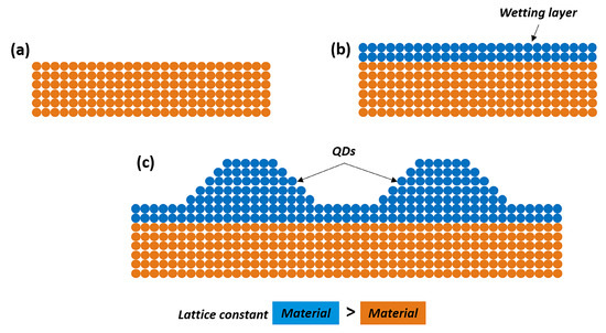
In the SK growth mode, the strain-induced formation of QDs occurs is driven by the lattice mismatch between the substrate and the epitaxially grown layer. Initially, a two dimensional (2D) wetting layer of the same material as QD is formed, after reaching a critical thickness of typically 1–2 monolayers (MLs), the growth deviates from a layer-by-layer growth and three dimensional (3D) islands are formed to accommodate the local strain. A schematic process of SKQDs formation is shown in Figure 1. The most typical material system used for the formation of QDs by the SK-growth process consists of a few monolayers of In(Ga)As deposited on a GaAs substrate where pure InAs has a lattice constant 7 % larger than that of GaAs. Initially, InAs forms a wetting layer on GaAs where growth evolves layer by layer. After reaching a critical thickness of about 1.7 MLs for the case of pure InAs deposited on GaAs, the stored strain energy due to the lattice mismatch changes the growth morphology from layers to islands. The critical thickness or critical strain is a function of the composition of the epitaxial layer. The strain relaxation can also lead to the formation of crystal defects, which strongly affect the optoelectronic properties of the QDs [30,31,32,33]. Developments in the growth techniques such as MBE or MOVPE in combination with decades of growth optimization made it possible to realize (nearly) defect-free QDs. Despite the huge success of this growth technique, which has been used to create QDs for various optoelectronic applications such as lasers and quantum information technologies [9,10,28], the available degrees of freedom to control the QD formation are limited. The SK-growth mode is only available for lattice-mismatched material systems and the presence of a 2D wetting layer coupled to the QDs is almost inevitable. The size and shape of the QDs mainly depend on initial layer thickness, growth temperature, and the lattice mismatch. Major constraints of SK-growth mode include the presence of 2D wetting layer, residual strain fields, strain driven intermixing of QDs with capping layer leading to a variety of composition profiles, energetically favored evolution of QDs with specific facets and dimensions, high aspect ratio (base to height), etc. The constraints of SK-growth can be largely eliminated by the fabrication of self-assembled QDs through droplet epitaxy.
Droplet epitaxy (DE) involves the formation and crystallization of metallic droplets to form QDs. DE was first proposed by Koguchi et al. [34], where they presented a new growth mechanism by splitting the group III and V deposition in the MBE growth chamber. The fundamental step in DE is the formation of group III droplets (Ga/In), which allows independent control over the size and density of the QDs. The droplet formation can be controlled by optimizing the group III molecular beam flux and the substrate temperature to obtain the desired size and density of the QDs. The surface reconstruction of the growth surface prior to the droplet deposition strongly influence the formation of nanostructures [35,36]. Later, the formed droplets are crystallized in a group V (As) rich environment forming the QDs, as shown schematically in Figure 2. The dissolution and adsorption of group V element by the droplet and the surrounding surface govern the process of DEQDs formation. The crystallization kinetics depending on group V flux and crystallization temperature plays a crucial role in determining the final shape (dots, disks, rings) and composition of the QDs [35]. Unlike in SKQDs, DEQDs can maintain their shape even after capping due to a reduced intermixing, which is largely driven by the lattice mismatch, between QDs and the capping layer. The DE growth mode has many advantages compared to SK growth mode: the ability to grow QDs without a wetting layer [37], independent control over QDs size and density during droplet deposition, both lattice-matched [38] and lattice-mismatched [39] materials can be grown by DE, precise control over shape engineering allows the formation of complex nanostructures. It is also possible to grow QDs via heterogeneous droplet epitaxy where two group III atoms are supplied simultaneously to form droplets and later crystallized to form QDs [40,41]. A detailed review of droplet epitaxy growth and optimization for various nanostructures can be found elsewhere [42,43,44,45].
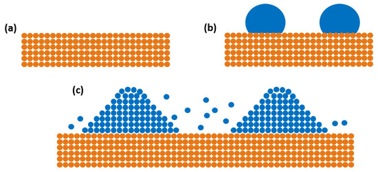
Figure 2. Schematic process showing the formation of DEQDs: (a) buffer layer; (b) deposition of group III droplets on the surface; (c) crystallization of formed droplets in group V rich environment.
3. Cross-sectional Scanning Tunneling Microscopy and Atom Probe Tomography of QDs:
The combination of cross-sectional scanning tunneling microscopy (X-STM) and atom probe tomography (APT) is a very powerful approach to study semiconductor heterostructures with atomic-resolution which provides detailed structural and compositional information on the system. A detailed structural and compositional analysis is crucial to optimize the QDs for various optoelectronic applications. Figure 3 shows a typical topographic filled-state image of a Gaussian-shaped GaAs QD in AlGaAs. One can also observe a GaAs-rich intrusion in the underlying AlGaAs matrix formed as a result of the local etching process at the solid-liquid interface after droplet deposition.
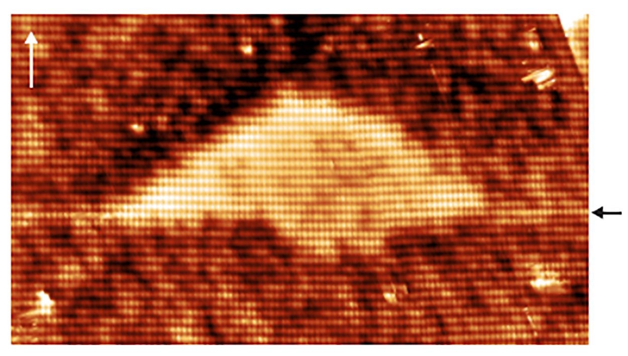
Figure 4 reveals the typical structure of the InAs/InP DEQDs grown by MOVPE. One can clearly observe the truncated pyramid shape of the QDs with well-defined facets. The QD has a base length of 27±0.5 nm with a height of 10.5±0.5 nm (11 BLs). We observed a good agreement in dimensions of QDs measured by both AFM and X-STM, especially the similar height of the QDs, indicating the absence of structural changes after the overgrowth. The color contrast in utoref{fig:topographicimage} represents the relative height of the STM tip from the surface. The brightness in the X-STM topographic image is due to the relaxation of the compressively strained InAs region after cleaving indicating the strained nature of the QD system, unlike the strain-free GaAs/AlGaAs DEQDs.
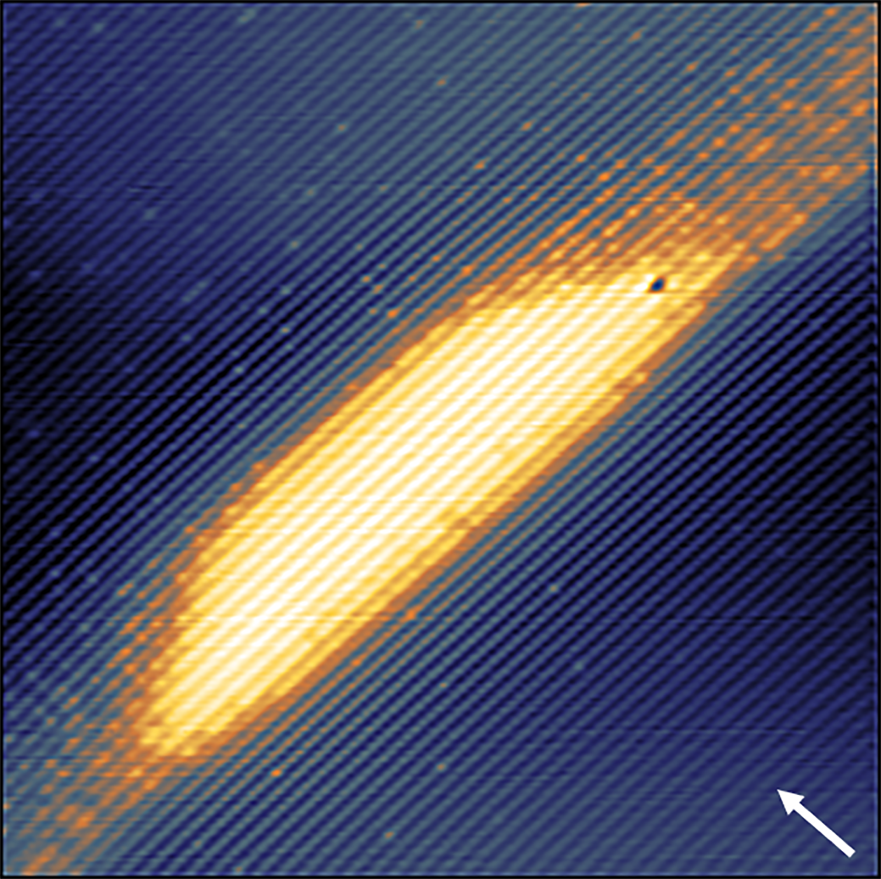
Figure 4. 30×30 nm2 filled-state topographic image of an InAs/InP DEQD (dark to bright contrast represents a height difference of 338 pm) taken at Vb=-3 V and It=50 pA revealing a truncated pyramid shape with well-defined side facets. The arrow indicates the growth direction [001].
On the other hand, APT provides a three-dimensional reconstruction of the nanostructures under-study providing detailed compositional analysis by identifying different chemical species through a mass spectrometer. In the published article, a more detailed analysis of APT of QDs is presented.
In summary, we presented a detailed review of the atomic-scale characterization of droplet epitaxy quantum dots by X-STM and APT. The structure and composition of strain-free GaAs/AlGaAs DEQDs were studied in detail in order to obtain a fundamental understanding of the growth mechanisms involved in droplet epitaxy. This is needed for further optimization of DEQDs for various optoelectronic applications. We presented an X-STM study of MOVPE grown strained InAs/InP DEQDs with atomic resolution. These InAs/InP QDs are considered as potential candidates for quantum communication networks as they emit in the low-loss wavelength region of 1.55 µm. The size, shape, and composition of the QDs were determined along with the presence of InAs etch pits in InP underneath the QDs. Droplet epitaxy is further explored to expand the options to create QDs with different materials where structural characterization techniques such as X-STM and APT are valuable tools to probe the embedded QDs at the atomic level.
This entry is adapted from the peer-reviewed paper 10.3390/nano11010085
References
- Keizer, J.G. Atomic-scale probing of metallic and semiconductor nanostructures. PhD thesis, Technische725Universiteit Eindhoven, 2012. doi:10.6100/IR728790.