Organic-inorganic hybrid perovskite materials have attracted tremendous attention as a key material in various optoelectronic devices. Distinctive optoelectronic properties, such as a tunable energy band position, long carrier diffusion lengths, and high charge carrier mobility, have allowed rapid progress in various perovskite-based optoelectronic devices (solar cells, photodetectors, light emitting diodes (LEDs), and lasers). Interestingly, the developments of each field are based on different characteristics of perovskite materials which are suitable for their own applications.
- peorvksite
- perovskite solar cell
- organic-inorganic halide structure
- perovskite light emitting diode
- perovskite photodetector
1. Introduction
With the expeditious growth of economic development and the demand for optoelectronic devices, organic-inorganic hybrid perovskites have attracted a great amount of attention as key materials in various fields, such as solar cells, light-emitting diodes [1,2,3], laser [4] and photodetectors [5,6]. By exploiting their superior properties, perovskite-based optoelectronic materials have developed at rapid speed [7,8,9,10]. Since the first demonstration was reported for perovskite solar cells (PSCs) in 2009 [11], the power conversion efficiency (PCE) of PSCs has improved considerably reaching ~25.5% within the past several years [12]. Moreover, the external quantum efficiency (EQE) of perovskite-based light-emitting diodes (PeLEDs) has now reached ~20% [13], which is comparable to that of organic light-emitting diodes (OLEDs) or quantum dot light-emitting diodes (QD-LEDs). Perovskite-based optoelectronic applications are now expanding and accomplishing astonishing performance in every field.
Perovskite material has an inorganic and organic hybrid structure with the main formula ABX3. The “A” and “B” denote two cations with different sizes, and “X” is an anion (Figure 1a). The common representative of these cations and anion is A = Cs+, CH3NH3+ (MA+), CH(NH2)2+ (FA+), CH3CH2NH3+, B = Pb2+, Sn2+, Cu2+, and X = Cl−, Br−, and I− (halogens). Based on the various combinations of A, B, and X, the perovskite material shows unique properties: a tunable band gap energy ranging from 1.6 eV (FAPbI3) to 3.1 eV (CsPbCl3) [14,15], long hole–electron diffusion length (>1 µm) [16,17], high charge carrier mobility [15,18], high photoluminescence quantum yields (PLQYs) [19,20] and low electronic trap states [21,22]. Thus, with such desirable features as light weight, flexible form, low cost, and solution-based processability, perovskite-based optoelectronic devices are leading in various fields.
Among various applications, PSCs are most widely being investigated. Most notably, PSCs with a PCE of 25.5% were produced by the Seok et al., which is comparable to the efficiency of commercialized traditional solar cells based on crystalline silicon and other combinations of inorganic semiconductors. In addition, benefitting from the near unity PL QY of perovskite nanocrystals, the EQE of PeLEDs has now reached 20% [13,24]. Since perovskite as emitting layer possesses a high degree of color purity for visible to infrared color ranges [25,26], PeLEDs promise the realization of full color displays with a wide color gamut exceeding the BT2020 standard. In laser and photodetector applications, perovskite also attracts a great deal attention due to its unique optoelectronic properties [27,28].
Halide perovskite crystals require different characteristics according to their applications. For example, in solar cells, low exciton binding energy is needed for efficient generation of electron-hole pairs, while LEDs require a highly radiative recombination process. The perovskite film properties such as layer thickness, surface characteristics, diffusion length, and trap state density largely differ from the chemical structure and film fabrication process. To identify the key issues in each perovskite-based application, we investigated the prerequisite factors in each application based on the representative studies. In this review, we briefly introduce the fundamental structure and characteristics of a halide-based perovskite layer and then highlight the key factors for achieving high performance in each application: solar cells, light-emitting diodes, lasers, and photodetectors. This is followed by a description of the remaining challenges. This review confirms the high potential of perovskite as a universal material solution for a wide range of optoelectronic applications, and enhances the understanding of key properties in each application for their practical commercialization.
3. Perovskite Solar Cells
With continuously increasing population along with high criteria for future renewable energy targets, there is intensive needs for environmental-friendly energies such as solar cells. Exploiting the suitable properties of light absorbing materials, such as large absorption coefficients, long charge diffusion lengths, and high carrier mobility, perovskite-based solar cells (PSCs) have achieved noticeable progress within 10 years and reached a certified efficiency of 25.5% in a single junction and of 29.1% in perovskite/Si multijunction solar cells. Since the PSCs have shown outstanding performance and cost-effective solution processability, the solar cell technology is entering the fourth generation [62,63,64,65,66]. Industrial level research, such as large-scale production, environmental-friendly production, and stable operation, for the practical use of PSCs is also investigated widely in various research institutes (e.g., The Swiss Center for Electronics and Microtechnology (CSEM) and National Institute for Materials Science (NIMS)) [67,68,69,70], which have recently achieved efficiency of 26.5% in perovskite/Si multijunction solar cells in large-area production [71]. In recent, Oxford Photovoltaics (Oxford PV) achieved 29.52% of PCEs with the perovskite on GaAs solar cells which was also certified by the US National Renewable Energy Laboratory (NREL).
Since the first demonstration by T. Miyasaka et al. in 2009 [32,72], there have been intensive studies to improve the performance of PCSs. The structure of PSCs can be separated as a mesoporous n-i-p structure, planar n-i-p (conventional), and planar p-i-n structure (inverted) [72,73]. These structures are meant to improve the charge extraction and transport characteristics, where the perovskite absorption layer is sandwiched between the electron-transport layer (ETL) and hole-transport layer (HTL). These charge transport layers (CTLs, both ETLs and HTLs) play crucial roles in extracting electron and hole charge carriers, which are generated from the perovskite absorption layer, and assisting the formation of a high crystallinity perovskite layer. Therefore, along with the uniform distribution of surface properties, the energy level of CTLs needs to be located at a barrierless position rather than at perovskite absorption layers.
The most critical factor in determining the performance of the PSCs is the perovskite film property. Various studies have been reported regarding the morphological distribution of perovskite films for high uniformity, high crystallinity, and high phase purity of the perovskite structure. Therefore, the perovskite film fabrication process is the most basic and important factor which directly affects the film quality. This section discusses the role of CTLs and the perovskite film fabrication process in the performance of PSCs.
3.1. Key Parameters for Solar Cells
The performances of solar cells are defined by the current density-voltage (J-V) characteristics under illumination. The main parameters, which indicate the performance of the device, are short-circuit current density (Jsc), open-circuit voltage (Voc), fill factor (FF), and most importantly, the power conversion efficiency (PCE). The Jsc is the current density when the devices are in zero bias conditions indicating the exciton dissociation property and charge transport property of the solar cells. Meanwhile, the Voc is the voltage difference measured between two electrodes when no current flows through the devices, indicating the built-in potential of solar cells. The FF and PCE are expressed as the following equations:
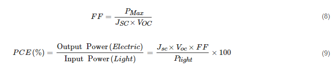
where PMax is the maximum power that the solar cells can produce and Plight is the irradiated solar energy. The FF measures the “squareness” of the J-V characteristics in solar cells, which is directly affected by the series and shunt resistances of the devices. The PCE is measured in standard conditions, which is a temperature of 25 °C and a 1 sun irradiation (100 mW/cm2) with an air mass of 1.5. The traditional silicon-based solar cells have shown an FF between 0.5 to 0.8 and a maximum PCE exceeding 25%.
3.2. Role of Charge Transport Layers
During the developmental progress of PSCs, much attention has focused on the development of the perovskite light harvesting layer. However, the CTLs are also crucial factors that determine both formation of perovskite film and performance of the devices. In the early stage of developing PSCs, H. Kim et al. [75] adopted mesoscopic TiO2 film as ETLs and 2,20,7,70-tetrakis-(N,N-di-4-methoxyphenylamino)-9,90-spirobifluorene (spiro-MeOTAD) as HTLs, achieving high efficiency (PCE ~ 10%) and stable PSCs (long-term stability tests for over 500 h). Their results emphasized the importance of CTLs in determining the performance of a PSC. There are several prerequisite factors [76,77] to function as ideal CTLs in PSCs: no energetic barrier for electrons and holes, high thermal stability, and non-toxicity. Until now, various ETLs (e.g., TiO2, SnO2, and ZnO) and HTLs (e.g., Spiro-OmeTAD, NiO, CuO, and PTAA) have been reported to achieve high performance PSCs.
The most important characteristic of CTLs is the energy level alignment with the perovskite absorption layer. For the energetically barrierless device configuration, the lowest unoccupied molecular orbital (LUMO) of the ETL should be located at a lower energy state than the perovskite layer and the highest occupied molecular orbital (HOMO) of the HTL should be located at a higher energy state than the perovskite layer. Moreover, the transmittance of CTLs in the UV-Vis region should be taken into consideration to maintain the number of photons during light exposure. The bottom layer of perovskite should have a smooth and uniform surface to obtain high crystallinity of the perovskite film, and the upper layer of the perovskite should use non-polar solvent not to damage the perovskite layer.
By taking all these considerations, transition metal oxide TiO2 is the most widely used for high performance PSCs [78]. Since TiO2 shows good chemical stability, a suitable energy level position compared with perovskites, and cost-efficient solution processability, various studies have reported the successful implementation of TiO2 as the ETL in PSCs. Recently, M. J. Paik et al. [79] proposed the high quality TiO2 layer by combining the TiO2 underlayer, which was formed by chemical bath deposition, and sprayed TiO2 colloids (Figure 5b). The dense and uniform TiO2 ETL-based PSCs have shown high performance with a PCE of 22.7%. Various studies have also widely investigated TiO2 with a bilayer ETL (e.g., TiO2/WO3, TiO2/SnO2, and TiO2/ZnO) [79,80,81] or applying metal doped TiO2 ETL (e.g., Li, Al, Nb, and Ni) to improve the optoelectrical property of the TiO2 ETL. Although a high annealing temperature has been raised as a challenging issue in the TiO2 ETL, various low temperature processable TiO2 ETLs with alternative fabrication methods (e.g., atomic layer deposition (ALD) and E-beam) have been reported [82,83,84].
3.3. Deposition Method of Perovskite Film
Two deposition processes have been most widely investigated in perovskite film fabrication: Solution process and thermal evaporation deposition process. In this section, we discuss perovskite film fabrication methods (solution process and evaporation process) and their effect on morphology and performance in PSCs.
3.3.1. Solution Process
In the solution spin coating process, one step and two step spin coating processes are the most commonly used in solution processes of perovskite film fabrication (Figure 6a). The one step spin coating process has the advantages of simplicity and low-cost processability, which is conducted using a perovskite precursor solution which is dissolved in polar solvents (e.g., DMF, DMAc, DMSO, and GBL) [85,86]. During the spin coating process and annealing process, the crystal structure of perovskite is determined by ionic interaction between anions and cations in the precursor. However, due to the slow crystallization process, partial aggregations and pinholes are generated, which results in low reproductivity in the film formation.
To enhance the uniform distribution of the perovskite film quality, a two-step spin coating process was proposed by K. Liang et al. [87] who used a two-step solution deposition method. They successfully fabricated CH3NH3BI3 (B = Pb, Sn) perovskite films by depositing BI2 film in advance and converting the film into a perovskite layer by adopting a CH3NH3I (MAI) solution. These sequential steps of BX2 and AX were investigated. J. Im et al. [88] reported high performance CH3NH3PbI3 PSCs with varying the MAI concentration. The concentration of MAI highly influences the cuboid size of perovskite films, which influences the optoelectronic characteristics of the perovskite absorption layer by altering the packing density of the crystal population and the light harvesting property. Therefore, by optimizing the cuboid size of MAPbI3 perovskite films, the PSCs achieved a high level of light harvesting and charge carrier extraction properties resulting a PCE of 17%. Similar studies have been reported on enhancing the enhancing film morphology. H. Ko et al. [89] and N. Ahn et al. [90] reported the effect of PbI2 concentration and annealing temperature in grain growth of perovskite film, resulting in a PCE of 15.8% and 14.3%, respectively (Figure 6c,d). Later, the crystal growth mechanism of perovskite in two step fabrication was quantitively investigated by Y. Fu et al. [91,92]. By adopting sufficient concentration of MAI in PbI2 films, the interface reaction initially formed a MAPbI3 structure along with producing PbI42−. After the saturation amount in the MAI solution, the PbI42− reacted with CH3NH3+ and slowly recrystallized to form a single crystal MAPbI3 perovskite structure. However, along with incomplete conversion of PbI2 residues, a long reaction time still remained as challenging issues which easily resulted in uneven formation of large crystals.
In both one step and two step processes, controlling the nucleation and crystal growth is highly emphasized for uniform formation of perovskite film morphology. One efficient way to solve this issue is inducing an anti-solvent during the formation of perovskite crystals. M. Xiao et al. [93] deposited chlorobenzene (CBZ) as an anti-solvent solution during one step spin coating of CH3NH3PbI3 (dissolved in DMF solvent) and achieved large crystalline perovskite grains with micron size. Compared to the conventional one step process, the PSCs with that used the anti-solvent process showed 192% enhancement in PCE. The role of the anti-solvent during the spin coating process controls the crystallization process by removing the residual precursor and enhancing uniformity of the perovskite film. Various kinds of solvents are adopted in anti-solvent processes. D. Son et al. [94] and N. J. Jeon et al. [95] used diethyl ether on MAPbI3 and toluene on FAPbI3, respectively, which showed remarkable improvement in performance of PSCs. With a similar principle, a mixture of anti-solvent was also investigated to form high quality perovskite film. J. Liu et al. [96] used a mixture of ethyl acetate (EA) and isopropyl alcohol (IPA) for spin coating a MAPbI3 perovskite precursor and achieved high PCE of 18.9%.
3.3.2. Thermal Evaporation Process
Fabricating a perovskite layer by the solution process inevitably accompanies a thermal annealing process on the substrates. However, the thermal annealing process limits the feasibility of choosing a substrate, which is especially essential in flexible optoelectronic devices. The thermal evaporation process can solve this issue and is also an efficient method to fabricate uniform and smooth perovskite film. Similar to the solution process, two methods are widely used to fabricate perovskite film via thermal evaporation: single source and dual source (or multiple-source) evaporation.
In the thermal evaporation process, the dual source evaporation method was reported earlier by M. Liu et al. [98] They presented CH3NH3PbI3−xClx mixed halide-based PSCs by evaporating MAI and a PbCl2 precursor in dual source simultaneously. The obtained perovskite film had a smooth and uniform morphology and the PSCs achieved a high PCE exceeding 15%. C. Meanwhile, Chen et al. [99] and S. Hsiao et al. [100] proposed CH3NH3PbI3-based PSCs in sequential steps of PbI2 and MAI in the thermal evaporation process, achieving perovskite film with a fine morphology. Since all inorganic perovskite (e.g., CsPbI3 and CsPbIxBr1−x) [101,102,103] has also been demonstrated by utilizing thermal evaporation, the thermal evaporation process attracted strong attention as an alternative method of solution processing.
This entry is adapted from the peer-reviewed paper 10.3390/cryst11010039