Plasmonic photocatalysts combining metallic nanoparticles and semiconductors have been aimed as versatile alternatives to drive light-assisted catalytic chemical reactions beyond the ultraviolet (UV) regions, and overcome one of the major drawbacks of the most exploited photocatalysts (TiO2 or ZnO). The strong size and morphology dependence of metallic nanostructures to tune their visible to near-infrared (vis-NIR) light harvesting capabilities has been combined with the design of a wide variety of architectures for the semiconductor supports to promote the selective activity of specific crystallographic facets. The search for efficient heterojunctions has been subjected to numerous studies, especially those involving gold nanostructures and titania semiconductors. In the present review, we paid special attention to the most recent advances in the design of gold-semiconductor hetero-nanostructures including emerging metal oxides such as cerium oxide or copper oxide (CeO2 or Cu2O) or metal chalcogenides such as copper sulfide or cadmium sulfides (CuS or CdS). These alternative hybrid materials were thoroughly built in past years to target research fields of strong impact, such as solar energy conversion, water splitting, environmental chemistry, or nanomedicine.
- Non-Titania Based Semiconductors
- Gold Plasmonics
- Heteronanostructures
1. Introduction
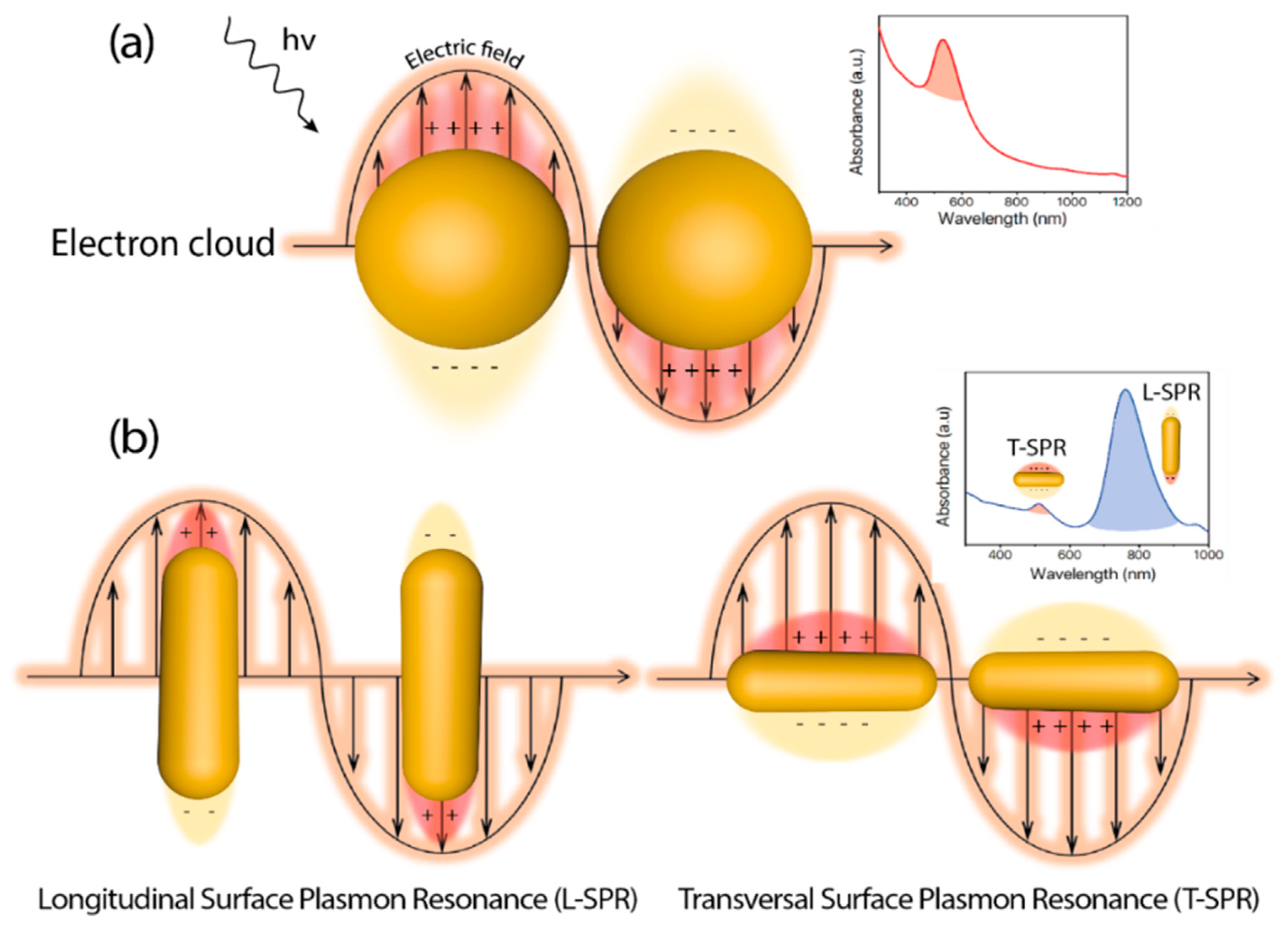
Since the first reported example of heterogeneous photocatalysis in 1911 applied to the degradation of Prussian Blue by ZnO powder and illumination [1], the degree of sophistication and complexity in photocatalyst design has experienced a huge development [2]. In heterogeneous photocatalysis, the process is initiated by the interaction between incident photons and the catalyst. The photon absorption by the catalyst (typically a semiconductor) leads to the promotion of valence band electrons into the conduction band, thereby creating electron-hole pairs. Those carriers can induce the subsequent generation of free radicals (e.g., hydroxyl (OH), superoxide (O2−)) to target specific chemical reactions. As a requirement, the energy of the incident photon (hν) must be equal or higher than the energy band gap (Eg) of the catalyst, meaning that the incident electromagnetic wavelength must be energetic enough to overcome the barrier to excite an electron from the highest occupied energy levels to the lowest unoccupied levels. Well-established semiconductor-based photocatalysts, such as TiO2 or ZnO possess high Eg values (3.05 [3] and 3.3 [4] eV, respectively) and are constrained to the more energetic ranges of the solar spectrum (i.e., UV window representing only up to 5% of the solar radiation) for an effective photoactivation. Abundant efforts have been devoted in the past decades to expand the photocatalytic response of heterogeneous semiconductor photocatalysts towards the visible and infrared ranges in order to maximize the absorption of the solar spectrum [5,6,7,8,9]. One of the most promising and explored strategies has consisted on the combination of semiconductor structures with noble-metal based nanoparticles [10,11,12]. Recent reviews available in the literature have deepened into the synergistic action of small metal nanoparticles decorating semiconductors and on how the controlled architecture of the latter may have a strong influence on the final photocatalytic outcome [13,14,15,16,17,18,19,20]. Another interesting aspect of metallic nanostructures correlates with their unique optical response that can be modulated upon variations of their specific size and morphology [19,20,21,22,23]. At the interface between the metal surface and other medium (with different dielectric properties), exist a phenomenon known as Localized Surface Plasmon (LSP) that consist on a coherent delocalized electron oscillation leading to the generation of an electromagnetic field both outside and inside the metal. An excitation with radiation of the right wavelength causes a resonance interaction and subsequent collective oscillation of conduction electrons, in the case of metallic materials, due to the restoring force between electrons and nuclei through Coulombic attraction (Figure 1). This phenomenon is called Localized Surface Plasmon Resonance (LSPR), and for metals like Au, Ag, or Cu, the LSPR may take place over a wide range of 400–1300 nm [24] as a function of their size and shape (Figure 1). Thus, metallic nanoparticles emerge as perfect candidates as visible near infrared (NIR) light harvesters to combine and improve the efficiency of semiconductor photocatalysts.
So far, TiO2 has been set as one of the most explored semiconductors to form hetero-nanostructures in combination with metals to overcome its limited photo-response beyond UV window [25,26] that can overcome its one of the most widely used semiconductors to carry out photocatalytic reactions. Systematic evaluation of Au-TiO2 hybrid systems exploring the role and influence of shape, specific configuration, heterojunction conformations, and so on, have been developed in the past years. Numerous and varied architecture designs have been successfully reported including core-shell (concentric and eccentric) [27,28], yolk-shell [29], Janus type structures [28], or even multi-component heterostructures [30,31] and their performance successfully tested towards energy and environmental applications [17,18,31,32,33]. The generation and assembly of these hetero-nanostructures offers multiple advantages but the number of alternative candidates to TiO2 still remains as an open challenge. The present review intends to overview the most recent advances described in the literature involving the design of hybrid photocatalysts combining plasmonic Au nanoparticles and non-titania based semiconductor coatings organized in a wide variety of nanoarchitectures (vide infra). Herein, we paid special attention to plasmonic hybrids that involved the selection of anisotropic Au nanostructures (mostly nanorods (AuNRs) and nanostars (AuNSs)) and a controlled growth of semiconductors beyond the most typically studied (i.e., TiO2 [27,34,35] or ZnO [5,36,37]). This approach allows a fine control of sizes for both metal and semiconductor, reduces the probability of recombination of carriers, and maximizes an intimate contact to form efficient heterojunctions [38]. In contrast, other methodologies lack sufficient control on the size and dispersion of metal nanoparticles or the corresponding supports. Furthermore, many times these semiconductor nanoparticle supports require additional tuning or post-treatments to ensure the exposure of preferential facets that do not necessarily prevent numerous bulk recombination events due to their inherent polydispersity [13]. Hence, recent research innovative trends, such as cancer therapy, require more accurate control of the photocatalysts dimension for proper internalization in cells and accurate reproducibility [39]. Therefore, we consider that the efforts made to improve the generation of novel plasmonic photocatalysts with a controlled size and distribution in a core-shell (or analogous nanoarchitecture) and/or semiconductor supports represents a very promising alternative to other metal-semiconductor configurations [13].
2. Metal-Semiconductor Hetero-Nanostructures: Different Configurations and Light-Driven Activation Mechanisms
A key feature of plasmonic photocatalysts is related with the photo-induced generation of highly energetic electrons (hot electrons) generated via LSPR [40]. The distribution of these hot electrons can be described by the Fermi equation using an elevated effective temperature [41]. After light absorption, LSPR decay may occur either radiatively, through re-emitted photons, or non-radiatively, for instance through transfer of hot electrons [42], generally through intraband excitations within the conduction band [40,43] thereby causing electrons from occupied energy levels to be excited above the Fermi energy. Hence, after coupling with metals, typical semiconductors used in photocatalysis can capture these hot electrons and generate reactive species by using visible-NIR light. The formation of metal-semiconductor heterojunctions allows hot electrons to be accepted into semiconductor conduction band and carry on the photocatalytic process (Figure 2a). The energetic barrier formed at the metal-semiconductor interface is called Schottky barrier [44]. Hot electrons are injected into semiconductor conduction band when their energy is superior to Schottky barrier energy (ESB) which is lower than the bandgap of semiconductor (Eg) [45]. After the hot electron generation, holes are also generated in the plasmonic structure as illustrated in Figure 2b. For this mechanism to occur there must be a good interaction between the metal and the support, which make critical the synthesis step of these hybrid materials.
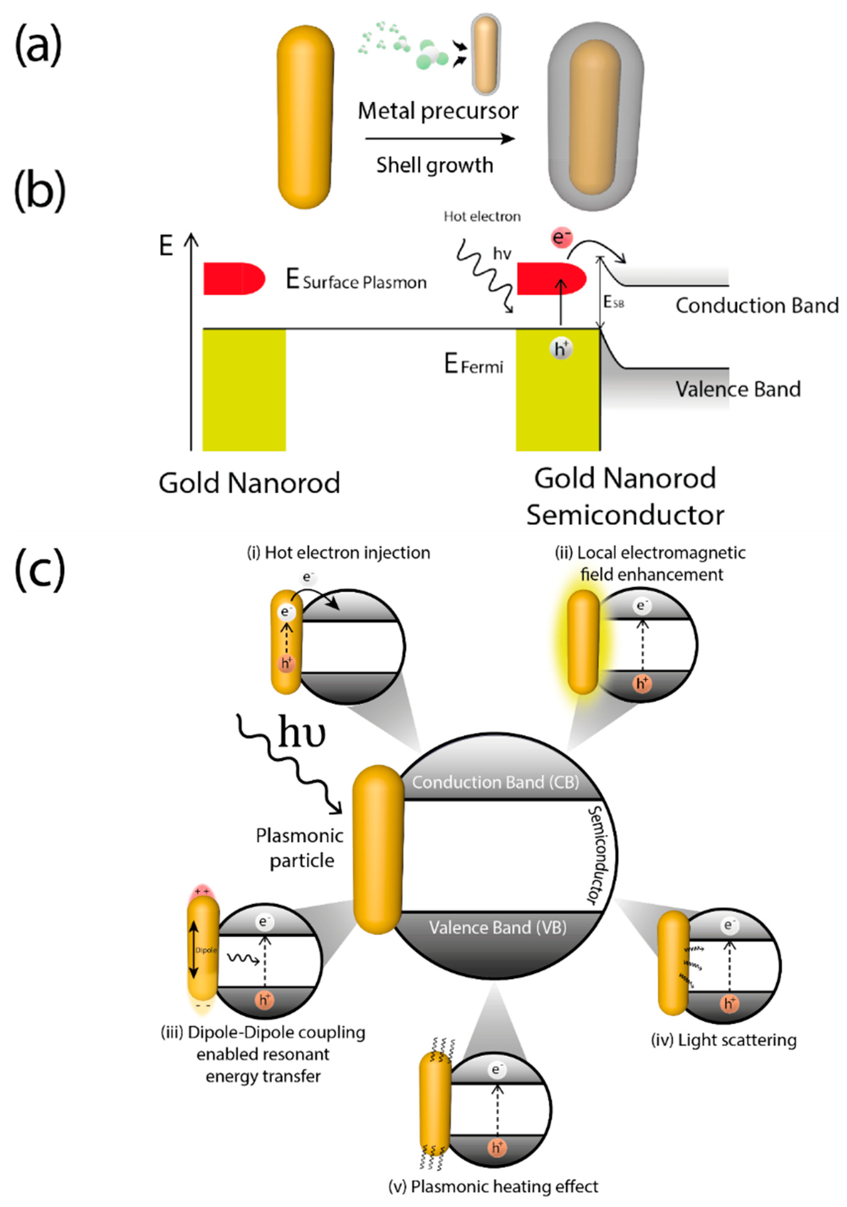
Nevertheless, several mechanisms could be involved independently or, most often, concurrently in photocatalysis using hybrid plasmonic materials [46]. Depending on the interaction of the plasmonic nanoparticle with the support and the electronic characteristic of the latter, plasmonic excitation can improve the photocatalytic properties of materials in several ways: (i) increasing absorption and scattering of light [47]; (ii) enhancing of the localized electric field [48]; (iii) hot charge carriers generation and transfer [49], already mentioned; (iv) dipole induction on non-polar molecules [50]; (v) local heat generation [46,51], depicted in Figure 2c.
Since nature, size, shape, and crystalline structure of the nanoparticle determine the energy of the LSPR [52] and in consequence the wavelength of the light used in photocatalysis, the control of those cited parameters is fundamental for the synthesis of suitable hybrid materials [53,54,55]. Concretely, the introduction of anisotropy in plasmonic-semiconductor systems adds a superior level of performance. Plasmonic Au cores exhibit a wide range of anisotropic nanostructures (nanoshells, nanorods, hollow spheres, nanoprisms, triangles, cubes, nanostars, urchins, etc.) with different LSPR [8,18,24,31,52,56] (Figure 3a). Typically, plasmon energy is concentrated on the sharpest edges of the anisotropic plasmonic nanostructures of high curvature [57,58,59] where light harvesting will take place more efficiently [60].
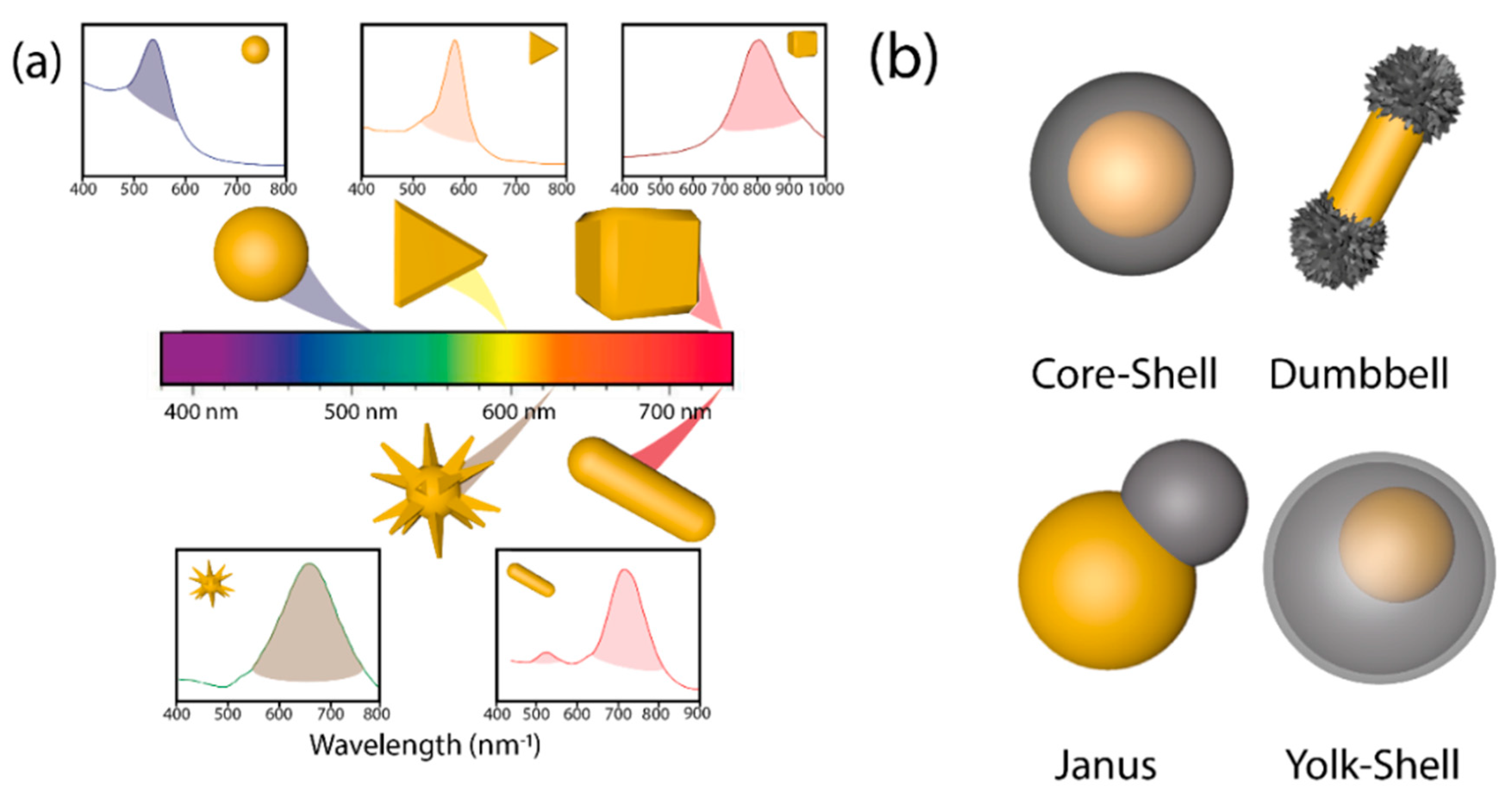
As shown in Figure 3b, it is possible to differentiate between core-shell, dumbbell, Janus, and yolk-shell configurations attending to the semiconductor distribution around the metallic cores [38] with several implications in their photocatalytic activity. Structures with exposed surfaces of both the metal and the semiconductors (i.e., dumbbell and Janus) exhibit a superior photocatalytic performance due to the continuous exposure of the reactants with the generated charge carriers (e−/h+) [27,40,60,61,62,63,64]. Different anisotropic heterostructures have been prepared with SiO2 [65], Pt [66,67], Fe2O3 [68], Cu2O [60], CeO2 [63], and TiO2 [27]. Yolk-shell structures (Figure 3b) are characterized by a hollow shell and an inner plasmonic core with several benefits for the photocatalytic process: (i) the presence of a hollow shell ensures higher specific surface area as it possesses an inner and external part. (ii) The small thickness of shells shortens charge diffusion distance, reducing possible bulk recombination processes, and (iii) void space present allows reflection of light inside the hollow shell, causing light scattering, and boosting the number of available photons [69].
This entry is adapted from the peer-reviewed paper 10.3390/catal10121459