Micro-electro-mechanical-systems (MEMS) acoustic emission (AE) sensors are designed to detect active defects in materials with the transduction mechanisms of piezoresistivity, capacitance or piezoelectricity. The majority of MEMS AE sensors are designed as resonators to improve the signal-to-noise ratio. The fundamental design variables of MEMS AE sensors include resonant frequency, bandwidth/quality factor and sensitivity. Micromachining methods have the flexibility to tune the sensor frequency to a particular range, which is important, as the frequency of AE signal depends on defect modes, constitutive properties and structural composition.
- MEMS
- acoustic emission
- piezoresistive
- capacitive
- piezoelectric
Note: The following contents are extract from your paper. The entry will be online only after author check and submit it.
1. Introduction
Acoustic emission (AE) is based on the detection of propagating elastic waves released by sudden stress-strain change in materials. Since the development of high-resolution instrumentation and data analysis tools, the AE method has been applied as a nondestructive evaluation tool in a variety of applications [1]. AE sensors form the primary link in detecting defects as shown in Figure 1. The energy released by an AE source propagates through the medium and reaches the AE sensor, which converts mechanical signal into electrical signal, defined as AE signal. Conventional AE sensors are made of bulky piezoelectric ceramics. While they have been used successfully in many applications, manual manufacturing, cost and size require moving the technology towards automated mass manufacturing of AE sensors with increased reliability, reduced cost and size.
Micro-electro-mechanical-systems (MEMS) are based on designing and manufacturing sensors and actuators using micromachining techniques (e.g., surface and bulk micromachining) which allow mass manufacturing with repeatable intrinsic characteristics. MEMS have enabled the design of sensors and systems using micromachining techniques since 1990s [2]. The application of the MEMS concept into AE sensing was first introduced by Schoess and Zook in 1998 [3]. Since then, there are several examples of piezoresistive, capacitive and piezoelectric MEMS AE sensors reported in the literature. With the introduction of a thin-film piezoelectric layer into MEMS manufacturing, potential towards to a commercial success for piezoelectric MEMS AE sensors increased. The first example of piezoelectric MEMS AE sensor was reported by Feng and Tsai in 2010 [4].
In this review article, the physical factors inherent to AE sensing and contributing to the design of MEMS AE sensors are discussed. The main characteristics of MEMS AE sensors such as resonant frequency, bandwidth/quality factor, sensitivity and other specifications pertinent to the transduction principles are presented. Transduction principles commonly used in MEMS AE sensing, including piezoresistive, capacitive (i.e., electrostatic) and piezoelectric, are discussed. Common MEMS geometries in the forms of beam or diaphragm and their design equations to tune to different frequencies are discussed. The history of MEMS AE sensors reported in the literature is presented. Conclusions and future outlook are discussed in the final section.
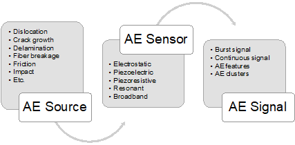
Figure 1. The simplified chain of acoustic emission (AE) sensing—AE sensor bridging AE source and AE signal.
2. Intrinsic Characteristics of AE Method Controlling AE Sensor Design
The AE method is a well-known nondestructive evaluation (NDE) method for (a) detecting the initiation of damage, (b) pinpointing the location of damage site, (c) qualitatively assessing the severity of damage and (d) classifying the damage mode using pattern recognition tools. Typically, resonant type AE sensor with narrowband frequency range is selected for (a), (b) and (c). While there are numerous examples using resonant AE sensors for the classification of damage modes, the proper source classification requires wideband or multifrequency AE sensors.
The AE source (related to energy release) and the structural medium carrying AE source to AE sensor (related to attenuation) control tuning the AE sensor into the right frequency, bandwidth, directional dependence and sensitivity. Once the target AE source and energy release are identified, the AE sensor characteristics can be defined. The AE sources depend on the materials’ composition. For instance, crack growth is a common AE source in metals while fiber breakage, matrix cracking and delamination are common AE sources in composites. Table 1 shows examples of AE sources in solids. As the structural medium and the defect mode are related, AE sensor should be designed by taking their interaction into consideration. As shown in Table 1, when a material has porous, anisotropic and viscoelastic properties, a low-frequency AE sensor is preferred to reduce the influence of attenuation and increase signal-to-noise ratio [5].
Table 1. Common AE sources in solids and typical AE sensors selected.
|
Material |
Common AE Sources |
Common AE Frequencies and Sensor Types |
Reference |
|
Metals |
Plastic deformation, internal friction, tensile crack, shear crack |
Wideband, 100–900 kHz High frequency resonant |
[6–8] |
|
Composites |
Matrix cracking, matrix splitting, matrix crazing, matrix lacerations, delamination, disbonding, fiber fracture, fiber pull-out and fiber/matrix interfacial failure |
Wideband to differentiate damage modes |
[9,10] |
|
Concrete |
Shear crack, tensile crack, corrosion |
Resonant, 40–100 kHz frequency range |
[11] |
|
Wood |
Longitudinal crack, fracture of fibers, inter-annual growth-ring crack |
Less than 100 kHz |
[12] |
|
Granular materials |
Grain-to-grain impact, fracture, solid and liquid bond rupture, grain friction |
Low frequency resonant near 20 kHz |
[13] |
Different defects generate different strain energy releases, which influence the selection of AE sensor sensitivity. Most literature selects the AE sensor based on previous literature, space limitation that controls the size of the specimen and available off-the-shelf sensors. A more physics-based approach is needed for selecting the proper AE sensor for sensing a particular defect in a material and energy release rate. In that aspect, state-of-the-art numerical models are combined with fracture mechanics in recent studies [14–16].
AE sensors are designed as resonant or broadband type. Resonant AE sensors, typically in the range of 20–500 kHz, have high quality (Q) factor (low damping), leading to narrow frequency bandwidth and high sensitivity. As they modify the input signal, they have limited applications for AE source characterization. However, they perform well in localizing AE sources in highly dispersive media (exhibiting frequency-dependent wave velocity) and pinpointing the initiation of the earliest stage of damage before visually seen. As MEMS AE sensors have smaller footprints than conventional AE sensors, they are typically designed as resonators to amplify the signal-to-noise ratio. Broadband AE sensors have a low Q factor, high damping, wide frequency bandwidth and low sensitivity. As they do not disturb the input signal, they are successfully implemented in identifying damage modes and source depth based on modal analyses. Figure 2 shows the comparison of a bulky piezoelectric AE sensor and a piezoelectric MEMS AE sensor. The conventional sensor includes piezoelectric ceramic sandwiched between electrodes and protected with wear plate and protection case. The piezoelectric MEMS AE sensor is made of a resonating silicon microstructure and a thin piezoelectric layer, which is mounted on a ceramic package. There is significant reduction in size and weight of MEMS AE device as compared to the conventional AE sensor.
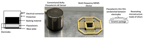
Figure 2. The comparison of conventional piezoelectric bulky AE sensor and piezoelectric micro-electro-mechanical-systems (MEMS) AE sensor designed by Ozevin’s research group.
3. Transduction Principles of MEMS AE Sensors
The dynamic input signal (displacement, velocity or acceleration) at the position of the AE sensor is converted into an electrical signal using three main transduction principles: piezoresistivity, capacitance and piezoelectricity. The geometric configurations can be lumped mass or distributed mass (i.e., diaphragm), as shown in Figure 3.
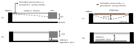
Figure 3. Different geometries and sensing configurations, (a) lumped mass + cantilever beam with piezoelectric or piezoresistive element, (b) lumped mass + cantilever beam with capacitive sensing, (c) distributed mass on a diaphragm with piezoelectric or piezoresistive element, (d) distributed mass on a diaphragm with capacitive sensing.
3.1. Piezoresistive MEMS AE Sensors
Smith [17] demonstrated the piezoresistivity property of silicon, which has been used as a transduction mechanism for mechanical MEMS sensors since then. The change in resistivity is proportionate to stress as follows [18]:
 |
(1) |
where is electrical resistance, is piezoresistivity coefficient, which depends on the crystal orientation and the dopant level, and is stress. The electrical resistance between two ends of a resistor is measured by
 |
(2) |
where is length, is cross-sectional area [19]. The change in resistance is related to
 |
(3) |
Assuming that the resistor is exposed to uniaxial strain, Equation (3) becomes
 |
(4) |
where is longitudinal strain, is Poisson’s ratio. The sensitivity is measured by the gauge factor () as
 |
(5) |
If the strain and the direction of current are both in longitudinal direction on <100> plane, then
 |
(6) |
where is Young’s Modulus of silicon. Here, represents . Combining Equations (5) and (6),
 |
(7) |
The n-type dopant would result in higher gauge factor as value is −102.2 × 10⁻¹¹ Pa−1, while it is 6.6 × 10⁻¹¹ Pa−1 for the p-type dopant. However, the p-type silicon piezoresistor has higher conductivity than the n-type silicon piezoresistor, which reduces the effect of temperature to the output signal [20]. The temperature dependence of piezoresistivity coefficients influences the measurement [21]. Therefore, temperature compensation approaches should be applied [22].
3.2. Capacitive MEMS AE Sensors
A capacitance is made of two conductors with opposite charges. A parallel plate capacitor is the most common configuration for AE sensing. The diaphragm forming the moving electrode of parallel plate capacitor can be built using a hexagonal [23], circular [24], square [25] or rectangular [26] shape.
Capacitance change due to dynamic stimulus is detected via change in capacitance (), which is related to dielectric constant (), overlapping area () or gap () between two capacitive layers. The capacitance between two parallel plates is measured by
 |
(8) |
As shown in Figure 3d, one layer is deposited on the substrate and the other layer is free to vibrate under inertial force. The change in capacitance is related to
 |
(9) |
If the dominant factor to capacitance change is gap change (), the produced displacement current () is calculated as
 |
(10) |
where is DC bias voltage, is time and is dielectric constant of air [25]. The operation of capacitive MEMS sensors requires constant DC bias voltage, which may introduce long-term durability challenges [27] in AE applications.
Figure 4 shows an example of a differential MEMS AE sensor achieved by designing two different gaps between capacitive layers that change due to in-plane excitation. The geometry can be modified to have different mass and spring elements, and multiple individual units can be connected to increase total capacitance and current output, which improves the signal-to-noise ratio. Capacitive MEMS AE sensors have advantages of large bandwidth, sensitivity, efficiency, integrated circuit compatibility and geometry flexibility.
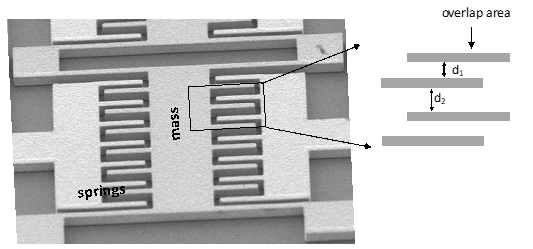
Figure 4. An example of a capacitive MEMS AE sensor for in-plane wave sensing [28].
The important variables for designing capacitive MEMS AE sensors are:
- Fundamental frequency, , which is controlled by stiffness and mass of microstructure. The geometry can be varied to tune to a particular frequency.
- Collapse voltage, which is defined as the bias voltage causing the failure of membrane. The value depends on stiffness, gap and overall area [29]. As the sensitivity increases with higher as shown in Equation (10), the design with higher collapse voltage improves the signal-to-noise ratio.
- Quality factor controls the bandwidth of a capacitive MEMS sensor. Quality factor depends on squeeze film damping between stationary and moving layers. High quality factor improves signal-to-noise ratio while it reduces the bandwidth. Squeeze film damping occurs due to the pressure of thin viscous fluid between two layers. The resonant frequency is also influenced by the damping level in the atmospheric condition [23,30].
- Dielectric charging, which is caused by the accumulation of unwanted charges stored and trapped on the dielectric surface [27]. This can increase the stiction of two layers, leading to permanent device failure. The failure can be prevented by depositing dielectric posts or a layer between two electrodes [21].
Post-manufacturing packaging of capacitive MEMS AE sensors has limited robustness. Wafer-level packaging can be adapted from capacitive MEMS ultrasonic transducers [31].
3.3. Piezoelectric MEMS AE Sensors
Since the development of thin piezoelectric film deposition on a substrate, piezoelectric MEMS sensors have been designed for sensing and actuating [32]. The thin-film piezoelectric layers have size constraints, stress from substrate, epitaxial growth affecting dependence on crystal orientation and substrate preparation to be compatible with piezoelectric thin-film [33]. The most common piezoelectric MEMS are resonating devices made of a piezoelectric layer deposited on a membrane operating at its resonance frequency. The piezoelectric AE sensor operates in the direct effect, which means that a mechanical strain or stress causes an electrical displacement. The coupled mechanical and electrical domains of bulk piezoelectric materials apply to thin piezoelectric films as
 |
(11) |
|
|
(12) |

where and are strain and stress tensors, and are electric field and displacement, represents elastic compliance and are piezoelectric coefficients. For thin-film piezoelectric MEMS devices, the most common coefficients are and , which are related to the electric field in 3 direction to strain, either in the same direction (3) or the orthogonal direction (1 or 2 due to symmetry) [34,35]. The directions 1, 2 and 3 are shown in Figure 5. The most important materials and geometric properties for sensing are piezoelectric coefficients, electromechanical coupling coefficient, mechanical quality factor, resonant frequency and residual stress.
- Piezoelectric coefficient and doping direction depend on ferroelectric (e.g., PZT) or nonferroelectric (e.g., AlN) materials. Ferroelectric materials are doped after deposition, while the doping orientation of nonferroelectric materials is controlled during the deposition [34]. Piezoelectric coefficients of common piezoelectric thin films can be found in [35].
- Electromechanical coupling factor is the ratio of the mechanical energy converted to the input electrical energy of the piezoelectric material. It can be calculated by motional capacitance and passive capacitance.
- Quality factor measures the mechanical damping of a microstructure where a high quality factor is needed for MEMS resonators [35]. Piezoelectric design has a higher quality factor than capacitive design, caused by squeeze film damping. The quality factor can be extracted from the impedance curve and half-power bandwidth formula as
 |
(13) |
where 

- Resonant frequency is controlled by mass and stiffness of microstructure. Further discussion is presented in the next section.
- The residual stress causing pretention to circular plate design can influence the resonant frequency [37]. If a thin diaphragm is selected for designing a low-frequency sensor (less than 200 kHz), geometric nonlinearities should be considered due to high aspect ratio of diameter to thickness [38]. To reduce the aspect ratio for designing low frequency piezoelectric resonators, Kabir et al. [39] designed a membrane connected with four beam elements and a mass made of an entire silicon substrate to reduce the resonant frequency of the microstructure as shown in Figure 5.
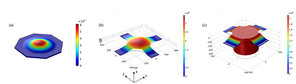
Figure 5. Three configurations to tune the resonant frequency, (a) diaphragm anchored around circumference to tune at MHz range, (b) diaphragm connected with flexible beams to tune the 100–500 kHz range, (c) silicon mass connected with flexible beams to tune less than 100 kHz. The color scale indicates the total displacement in micrometers.
This entry is adapted from the peer-reviewed paper 10.3390/app10248966