Emerging technologies, such as smart wearable devices, augmented reality (AR)/virtual reality (VR) displays, and naked-eye 3D projection, have gradually entered our lives, accompanied by an urgent market demand for high-end display technologies. Ultra-high-resolution displays, flexible displays, and transparent displays are all important types of future display technology, and traditional display technology cannot meet the relevant requirements. Micro-light-emitting diodes (micro-LEDs), which have the advantages of a high contrast, a short response time, a wide color gamut, low power consumption, and a long life, are expected to replace traditional liquid-crystal displays (LCD) and organic light-emitting diodes (OLED) screens and become the leaders in the next generation of display technology. However, there are two major obstacles to moving micro-LEDs from the laboratory to the commercial market. One is improving the yield rate and reducing the cost of the mass transfer of micro-LEDs, and the other is realizing a full-color display using micro-LED chips.
- micro-LED,full-color display,mass transfer,color conversion,monolithic growth
1. Introduction
Augmented reality (AR) and virtual reality (VR) technologies are developing rapidly with the maturity of artificial intelligence and image recognition technology. Among them, near-eye displays (NEDs) and head-mounted displays (HMDs) are key devices for AR/VR products. At present, mainstream near-eye displays are mostly liquid-crystal displays (LCDs) and organic light-emitting diodes (OLEDs) [1]. However, LCDs have a slow response speed, poor conversion efficiency, and low color saturation and are gradually being replaced by OLED displays that have the advantages of self-luminescence, wide viewing angles, high contrast, low power consumption, and fast response speeds. In addition, the excellent flexibility and transparency of OLEDs also provides a broad space for emerging electronic products, such as curved displays, smart watches, and folding displays [2]. However, due to the characteristics of OLED’s organic light-emitting materials, defects, such as their rapid aging, short life span, and low color purity, have been gradually exposed [3]. Therefore, both LCD and OLED technologies have technical limitations and cannot perfectly adapt to the display performance of AR/VR. Mini-LEDs and micro-LEDs, which inherited the characteristics of inorganic LEDs and have micron-level dimensions, have become popular as the next generation of display technology. Micro-LED technology was first proposed by a research team at Texas Tech University in 2000 [3]. The pixel pitch limit to distinguish Mini-LEDs and micro-LEDs is 100 μm, and those smaller than 100 μm are defined as micro-LEDs [4]. With the advancement of the manufacturing process, the pixel size and pixel pitch of micro-LEDs have gradually decreased from 100 μm. In terms of functionality, Mini-LEDs are mainly used as backlight displays [5,6], while micro-LEDs [7], which have the advantages of a high contrast, a high response speed, a wide color gamut, low power consumption, and a long life, are considered to be an ideal display technology for AR/VR. Table 1 provides a comparison of micro-LED with other display technologies.
Table 1. Performance comparison of micro-light-emitting diodes (micro-LEDs) with liquid-crystal displays (LCD) and organic light-emitting diodes (OLED).
| Display Technology | LCD | OLED | Micro-LED |
|---|---|---|---|
| Luminous mode | Backlight module | Self-luminous | Self-luminous |
| Luminous efficiency | Low | Medium | High |
| Brightness (cd/sqm) | 3000 | 1000 | 10,000 |
| Contrast | 5000:1 | 10,000:1 | 1,000,000:1 |
| Life (hours) | 60 K | 20–30 K | 80–100 K |
| Color rendering | 75% NTSC | 124% NTSC | 140% NTSC |
| Response time | Millisecond level | Microsecond level | Nanosecond level |
| Energy consumption | High | About 60–85% of LCD | About 30–40% of LCD |
| Pixels per inch (PPI) | 800 | 500 | >2000 |
NTSC—National Television Standards Committee.
The world’s first micro-LED display was launched by Sony at the 2012 Consumer Electronics Show (CES) exhibition and was called crystal light-emitting diodes (CLED). This display has a size of 55 inches, with unprecedented picture color, response speed, and high contrast. In the following years, Sony officially launched this technology to the market, successfully opening the door to the commercialization of micro-LED display technology. In 2018, Samsung showed off the world’s first spliced 146–inch micro-LED TV, “the Wall”; X-Celeprint also demonstrated their 5.1–inch micro-LED full-color display, and LG introduced a 175–inch micro-LED display in the same year. In 2020, many micro-LED companies, such as Jade Bird Display, Lumiode, Plessey, PlayNitride, etc., have begun to gradually launch their own products, and Vuzix is expected to launch its first micro-LED glasses next year. PlayNiride also plans to build its second micro-LED production line, which will increase its productivity by 2–3 times. It can thus be seen that micro-LED has gradually stepped onto the stage of the display field.
2. Chip Transfer and Bonding
The most direct solution to achieve a full-color micro-LED is to epitaxially grow RGB micro-LED chips on GaN and GaAs wafers. Then, through large-area and high-precision transfer technology, the three-color micro-LEDs are bonded onto the same drive substrate to form an RGB micro-LED display array. Independent addressing and Pulse width modulation (PWM) technology can control the brightness and grayscale of each RGB pixel, which can realize a full-color of the micro-LED display.
2.1. Horisontally and Vertically Stacked Micro-LED Structures
There are two main arrangement structures for obtaining a full-color micro-LED array in this way: a horizontal arrangement structure and a vertical stack structure. In 2016, Deng et al. used chips on board (COB) technology to integrate RGB three-color micro-LEDs on a transparent quartz substrate (LEDoTS) with addressable pixels to form a color display [29]. The display substrate area was 5 × 5 mm2, and the resolution was 5 × 5 × 3. The side length of each RGB pixel was 1 mm, and the emission wavelengths of the RGB three-color LEDs were 450 nm, 565 nm, and 630 nm, respectively. The planar structure is shown in Figure 1a. Field-programmable gate array (FPGA), as the main control unit of a LEDoTS color display, controls the cathode constant current driver and the anode scan driver through dynamic scanning and PWM modulation to realize the independent addressing and dimming of each RGB sub-pixel. Its working principle is shown in Figure 1b. In 2017, the authors used the same technology to develop a smaller 8 × 8 × 4 R-G-B-IR micro-LED array [30]. The dimensions of the blue, green, red, and infrared LEDs were 230 μm × 385 μm, 210 μm × 210 μm, 225 μm × 225 μm, and 285 μm × 285 μm, respectively. The peak wavelengths of the emission spectrum were 460 nm, 572 nm, 630 nm, and 850 nm, and the maximum half-wavelength was less than 30 nm.
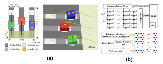
Figure 1. (a) Horizontally arranged red, green, and, blue (RGB) three-color light-emitting diodes (LED) pixel plane structure; (b) horizontally arranged RGB micro-LED array working principle. Reproduced from [29], with permission from Institute of Electrical and Electronics Engineers, 2016.
Vertically stacked LED structures have been studied for a long period of time [31,32]. For micro-LED displays with high resolution on a limited substrate, the area of the substrate occupied by each RGB pixel of the vertically stacked RGB micro-LED array is reduced by 2/3 compared to the horizontal arrangement structure. In 2017, Kang et al. proposed a color-tunable display composed of blue and green passive matrix micro-LED arrays stacked vertically [33]. This display array can independently address each pixel, and, by modulating the PWM duty cycles of the blue or green micro-LED drive voltages, the light-emitting wavelengths of each pixel can be changed from 450 nm to 540 nm, as shown in Figure 2a.
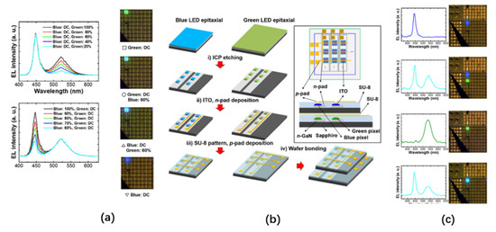
Figure 2. (a) Electroluminescence (EL) spectra measured by changing the Pulse width modulation (PWM) duty ratios of the green sub-pixels and blue sub-pixels, and microscope images at the same pixel positions of the micro-LED array under different PWM duty ratios; (b) manufacturing steps of vertically stacked passive matrix micro-LED arrays; (c) four emission modes of vertically stacked passive matrix micro-LED arrays. Reproduced from [33], The Optical Society, 2017.
2.2. Elastomer Stamp Transfer
Elastomer stamp transfer technology can transfer a large number of microstructures from one substrate to another at high speed [35,36,37,38]. Rogers’ team initially used elastomer stamps for large-scale transfer printing [11]. This technology closely contacts the micro devices on the donor substrate with an elastomer stamp array matching the pitch of the micro devices on the donor substrate. Through the van der Waals force between the elastomer stamp and the latter, the micro device is picked up and transferred to the receptor substrate. The picking and placing of the elastomer stamp on the microstructure are determined by the peeling speed after the two contact each other. By pulling the stamp away from the donor substrate at a sufficiently high peeling speed (usually faster than 10 cm/s), the elastomer stamp can generate strong adhesive force to adhere the microstructure to the surface of the stamp and remove the target device from the donor substrate. When the peeling speed of the stamp is less than 1 mm/s, the microstructure will be separated from the stamp and remain on the receptor substrate instead of being adsorbed by the stamp.
In 2005, Lee et al. proposed two elastomer stamp transfer methods that can realize the selective transfer of thin film transistors (TFT) to rigid or flexible substrates [39]. The transfer processes of these two methods are shown in Figure 3. The first method uses polydimethylsiloxane (PDMS) as an elastomer stamp, which comes into contact with the micro-silicon structure on the silicon-on-insulator (SOI). Due to the strong automatic adhesion of the PDMS, the Si microstructure in the corresponding area of the protruding PDMS part will be selectively detached from the SOI surface. After that, the PDMS part comes into contact with a polyethylene terephthalate (PET) receiving plate coated with polyurethane (PU), and then ultraviolet/ultraviolet ozone (UV/UVO) exposure is performed on the PET side to fully cure the PU and strengthen its bond with the Si microstructure. Lastly, the PDMS is peeled off, and the microstructures are bonded. The second method is to use decal-transfer lithography (DTL) technology based on method one, using a flat, unmolded PDMS plate for selective transfer. The adhesion strength of the plate is enhanced by photochemical treatment. Afterward, selective masking and an UVO treatment are performed on the surface of the PDMS plate. By exposing the plate, the PDMS coating with changed photochemical properties comes into contact with the SOI wafer and is heated to 70 °C for 30 min. Finally, the PDMS is stripped from the SOI, thereby selectively transferring the Si microstructure from the SOI wafer to the plate with the PDMS.
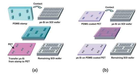
Figure 3. (a) The transfer printing step using polydimethylsiloxane (PDMS) and (b) the elastomer stamp transfer step using decal-transfer lithography (DTL) technology. Reproduced from [39], with permission from John Wiley and Sons, 2005.
2.3. Laser-Induced Transfer
Laser-induced forward transfer (LIFT) is a high-resolution single-step direct printing technology. LIFT can achieve surface micro-patterning or the partial deposition of solid or liquid materials and is widely used in selective printing of electronic devices, such as organic TFT, OLED, Micro-Electro-Mechanical System (MEMS), and sensors [42,43]. The steps for transferring solid-state pixels are shown in Figure 4a. The transfer of solid-state pixels is done to irradiate a thin layer of absorbing material deposited on a transparent substrate with a pulsed laser. After irradiation, light–matter interactions occur at the interface between the substrate and the absorbing material, causing the local pressure of the irradiated area to increase rapidly. In this way, a small pixel on the absorbing material film is separated from the donor substrate and deposited on the opposite receiving substrate. Because the size and shape of the emitted material are controlled by the size and shape of the incident laser spot, LIFT can not only deposit typically sized devices but can also transfer microstructures.
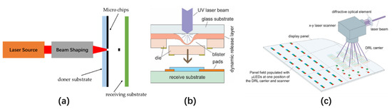
Figure 4. (a) Principle of laser-induced forward transfer technology. Reproduced from [43], with permission from Elsevier, 2016; (b) principle of massively parallel laser transmission technology launched by Uniqarta and (c) Massively Parallel Laser-Enabled Transfer (MPLET) technology that uses diffractive optical elements to transmit multiple pixels in parallel. Reproduced from [44], with permission from John Wiley and Sons, 2018.
3. Color Conversion Technology
Color conversion technology is a method that can realize a full-color micro-LED display without a mass transfer and is utilized in two main ways. One is to use a UV or blue micro-LED array as the excitation light source and place colored phosphors, quantum dots (QDs), or other light-emitting nano organic materials onto an RGB color conversion layer covering the micro-LED light source to achieve multi-wavelength light emissions, as shown in Figure 7. If the UV micro-LED is the light source, it is necessary to use three conversion materials to produce the RGB three-color conversion layers; if the excitation light source is a blue LED, only the corresponding red and green conversion layers are needed to realize the full-color display of the micro-LED.

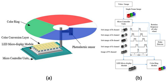
An alternative method of implementing a full-color display is to first convert the blue micro-LED into white light and then cover the RGB filter on the white light source to obtain the RGB tricolor sub-light source. This method does not need to distinguish between the RGB pixels of the micro-LED array but only needs to prepare the corresponding RGB pixel filters, making the preparation simple and low-cost. In 2019, Xu et al. proposed a full-color LED micro-display system based on time division multiplexing with dynamic color filters [52]. The whole system is composed of a micro-LED display module, a color conversion layer, a microcontroller unit (MCU), and a dynamic color filter module, as shown in Figure 8a. The area of the micro-LED display module is 7 mm × 11 mm, the resolution is 920 × 480, and the pixel pitch is 12.8 μm; when constructed, this module can emit 450 nm blue light. The color conversion layer with a thickness of less than 3 μm is composed of QDs, which are coated on the micro-LED array to convert blue light into white light. The core component of this system is the dynamic color filter, which consists of four-color blocks of red, green, blue, and colorless. By rotating the color filter, the MCU outputs a gray-scale image of the corresponding channel according to the duty ratio of the different colors, thus displaying the color image using a time-division multiplexing method. The working process is shown in Figure 8b. However, the filter absorbs 2/3 of the emitted light, which greatly reduces the luminous efficiency of the micro-LED array, so the first method with separate light conversion materials is more suitable for the development of color conversion micro-LED displays.
The material of the color conversion layer is generally phosphors or QDs. The phosphor is composed of some wide band gap materials (such as oxides, nitrides, and sulfides) and a small number of doping ions (transition metals or rare earth compounds). Although phosphors have mature preparation technology, high thermal and chemical stability, and a good quantum yield [53], their particle size is in the micron level, making them difficult to uniformly coat on micro-LED pixels at the same size level, which will affect the color conversion efficiency and uniformity of the micro-LED display. In contrast, the rapidly developed QDs of recent years have a nanometer size, a narrow emission spectrum, a wide absorption spectrum, higher luminous efficiency, etc. Therefore, QDs are more suitable for full-color micro-LED displays. This section will introduce the methods used for achieving full-color micro-LED displays through the phosphor color conversion layer, the QD color conversion layer, and other color conversion technologies over the past ten years.
This entry is adapted from the peer-reviewed paper 10.3390/nano10122482