Electroplating has been favored to date as a surface treatment technology in various industries in the development of semiconductors, automobiles, ships, and steel due to its advantages of being a simple, solution-based process, with low cost and high throughput. Recently, classical electroplating has been reborn as an advanced manufacturing process for functional materials by combining it with unconventional optical three-dimensional (3D) nanofabrication techniques capable of generating polymer templates with high-resolution 3D periodic nanostructures.
- electroplating
- nanostructure
- nanofabrication
Note:All the information in this draft can be edited by authors. And the entry will be online only after authors edit and submit it.
1. Introduction
Around the 2000s, with the explosive increase in interest in the experimental realization of three-dimensional (3D) photonic crystals in the academic world, various unconventional techniques optimized to manufacture nanostructured materials with 3D structural periodicity at the sub-micron level were developed. The proposed 3D nanofabrication techniques can be broadly classified into two types, non-optical and optical approaches. Non-optical approaches include colloidal self-assembly [1–6], block copolymer lithography [7,8], direct ink writing [9], and layer-by-layer transfer printing [10,11]. These methods have the advantage of being able to easily create 3D periodic nanostructures with a simple experimental setup, but they inherently have limitations in industrial aspects such as patterning resolution, defect control, and mass production. On the other hand, optical approaches derived from photolithography, which is a mature technology in the semiconductor industry, can precisely control 3D periodic nanostructures with high resolution and have great potential to advance into industrial technologies. The high resolution of optical manufacturing technologies is due to the nature of light that can be highly focused and precisely controlled through delicate optical components. Various interesting approaches such as direct laser writing (DLW) [12–21], multi-beam interference lithography (MBIL) [22–27], and proximity field nanopatterning (PnP) [28–41] have emerged as optical 3D nanofabrication techniques and have successfully demonstrated their ability to implement different classes of 3D periodic nanostructures.
Recently, the research trend related to 3D nanofabrication and nanostructures has started to change slightly. The mainstream of previous research has focused on optical applications including 3D photonic crystals based on the structural periodicity of 3D nanostructures fabricated through 3D nanofabrication techniques. In addition to the unique optical properties that stem from structural periodicity, many scientists and engineers have begun to pay attention to the porous nature of structures created through 3D nanofabrication techniques. In particular, optical approaches such as DLW, MBIL, and PnP have a differentiated ability to precisely control pore size at the nanoscale and to align sub-micron pores three-dimensionally. Through this, it is possible to design the porosity of the material and to control the microscopic flow of liquid/gaseous substances or electron/phonon, which may have a profound impact on the overall performance of the electronic and electrochemical systems [42–44]. Many existing electrochemical devices facing the limit of performance improvement seek to employ such well-designed porous materials with large surface-to-volume ratio (SVR) because their performance is primarily dependent on the degree of surface chemical reaction. Moreover, the porous network of a 3D periodic nanostructure allows it to serve as a matrix capable of continuously carrying heterogeneous materials to realize multifunctional materials [31,38,45,46]. Such types of bicontinuous nanocomposites have the advantage of being able to independently control heterogeneous physical functions that cannot be achieved through traditional mixture-based nanocomposite systems [45].
In response to these technical demands, research on the development of functional materials with 3D periodic nanostructures for non-photonic applications is actively progressing by combining unconventional optical 3D lithography with conventional thin film deposition techniques such as chemical vapor deposition (CVD), physical vapor deposition (PVD), atomic layer deposition (ALD), sol–gel reaction, and electrochemical deposition. Since most 3D periodic nanostructures created through optical 3D nanofabrication techniques are inevitably composed of photoreactive polymer-based dielectrics, a material conversion step is required to convert them into functional inorganics or composites that can be used for electronic or electrochemical devices. Among various infiltration systems, electroplating, which can grow an inorganic thin film on a conductive substrate through a reduction reaction using electrical energy, has already been widely used for industry because of its advantages in terms of process simplicity, chemical diversity, low cost, and high throughput [47]. In particular, a bottom-up growth behavior from a seed layer makes electroplating very well suited for densely filling 3D nanostructured porous templates with functional inorganics. In addition, unlike other infiltration techniques that generally require a high-temperature environment [48], electroplating, which is based on a solution process near room temperature, can transform the constituent materials of 3D nanostructures without causing heat-induced structural collapse to the polymer template, with a relatively low melting point generally below 200 °C.
Through this strategy, several research groups have successfully reported a new class of functional materials produced by the combination of optical 3D nanofabrication and electroplating. The form of the proposed materials can be divided into two types: 1) 3D bicontinuous organic–inorganic composites and 2) porous inorganics. The former is generated when the porous network of the polymer template is filled with a heterogeneous material, and in this state, the latter may be generated when the polymer template is completely removed through a chemical or physical process [49]. These two types of 3D nanostructured materials are contributing to the innovation of existing electrochemical or energy-related device architectures, including batteries, catalysts, and thermoelectric devices, and fundamentally improve their performance limits imposed by planar architectures. As such, research on the development of functional materials with 3D periodic nanostructures through the combination of optical 3D nanofabrication and electroplating is gradually maturing, but the latest research cases have not been organized yet. In this mini review, we would like to introduce the recent achievements related to 3D functional nanostructures generated by combining advanced optical 3D lithography and electroplating and discuss in-depth important technical issues that should be considered critical in the fabrication process [50–52].
2. Fabrication Strategy for Functional Materials with 3D Periodic Nanostructures
The manufacturing of functional materials with 3D periodic nanostructures covered in this review is essentially based on a template-assisted synthesis that utilizes a porous template with interconnected open pores. This template-assisted synthesis consists of two major steps: 1) preparing a porous polymer template with 3D periodic nanostructure via optical 3D lithography (Figures 1a to 1c) and 2) bottom-up filling the porous template with a heterogeneous inorganic material via electroplating (Figure 1d). If a porous inorganic material with high SVR is required, removal of the polymer template can optionally be performed as a third step. In the following, we discuss the technical issues that need to be considered significantly in the process, along with a detailed description of each step.
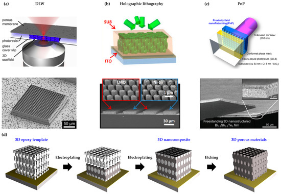
Figure 1. (a) Schematic illustration (top) and SEM image (bottom) of a 3D scaffold synthesized by DLW (direct laser writing) (reprinted with permission from [21]. Copyright 2014 Elsevier); (b) Schematic illustration (top) and SEM image (bottom) of 3D nanostructured anodes and cathode produced by holographic lithography (reprinted with permission from [53]. Copyright 2015 The National Academy of Science); (c) Schematic illustration (top) and SEM image (bottom) of 3D nanostructured thermoelectric materials fabricated by PnP (proximity field nanopatterning) (reprinted with permission from [38]. Copyright 2017 The Royal Society of Chemistry); (d) Schematic illustration of the fabrication process of 3D functional nanostructured materials.
2.1. Preparation of 3D Nanostructured Polymer Templates via Optical 3D Lithography
Since the early 2000s, various optical 3D nanofabrication techniques have been developed to experimentally implement 3D photonic crystals requiring precise structure control at the nanoscale. In principle, optical 3D lithography techniques are originated from photolithography in semiconductor processes and treat photoreactive polymers in different ways. Essentially, the resolution and reproducibility of 3D nanostructures formed by optical 3D lithography are superior compared to other self-assembly-based 3D nanofabrication techniques. In addition, optical 3D lithography has a high degree of freedom of 3D nanostructures that can be produced and has the potential to advance into mass production technology. Such optical 3D lithography techniques can be largely divided into two types: 1) serial process and 2) parallel process. One of the serial processes is DLW, which uses a highly focused laser beam to draw a 3D feature in photoresist. Interference-based lithography is a representative parallel process that generates multilayered, complex 3D nanostructures in a single exposure.
First, DLW is also called two-photon lithography or stereolithography. In principle, DLW can be regarded as a type of 3D printing technology capable of constructing 3D nanostructures with sub-100 nm resolution [16]. An ultrafast, high-power laser beam is tightly focused through a high-magnification objective lens within the volume of a transparent photoreactive polymer, and the exposed region is locally polymerized as a result of absorbing two photons simultaneously. Based on drawings designed through computer-aided design (CAD) or computer-aided manufacturing (CAM), the laser beam can travel along a given path to create a continuous 3D networked polymer. Unpolymerized residues can be removed by a developing solvent. DLW is very advantageous when arbitrary 3D nanostructures with high resolution are required. However, since DLW is based on a serial process, it inherently has a fatal disadvantage in that the production speed becomes extremely slow as the overall volume of the product increases or the size of the unit structure decreases [54]. It takes approximately several days to fabricate a 3D periodic nanostructure with a unit cell of several hundred nanometers in cm size. The development of photoresist capable of absorbing two photons is challenged, and the power threshold for causing two-photon polymerization is very high as well.
On the other hand, MBIL, also called holographic lithography, which uses 3D interference patterns of light generated by overlapping multiple coherent beams at one point, can produce 3D periodic nanostructures in mm or cm size with a single, short exposure [55–58]. The exposure time depends on the sensitivity of the photoreactive polymer and the intensity of the laser, which is within a few seconds. In order to create 3D periodic nanostructures, interference of at least four beams is required, and various symmetric structures can be generated by controlling the intensity, incident angle, or polarization of each beam. In comparison with DLW, although the resolution of MBIL is slightly lower, it definitely has improved productivity. However, MBIL requires a very complex configuration of expensive optical components because at least four coherent beams have to be superimposed, and the reproducibility is extremely poor due to low vibration tolerance. To solve these issues, a single beam-based interference lithography using a well-designed microprism has been developed, but the degree of structural freedom is still somewhat inferior [59].
PnP, also called phase-mask interference lithography, which uses diffraction and interference generated from a transparent phase mask, can be regarded as a high-resolution interference lithography technique that has evolved to be closer to a mass production process [29–32,34–36,60,61]. The phase mask used for PnP contains a relief grating structure on its surface whose grating periodicity is close to the wavelength of incident light to generate far-field diffraction. Near the mask surface, a 3D periodic intensity distribution of light can occur as a result of interference of diffraction orders. This unique optical phenomenon is called the Talbot effect, discovered by Henry F. Talbot in 1836, and was reborn in 2004 as a key technical principle of PnP, which is an advanced type of 3D optical lithography. In order to capture the Talbot interference within a photoresist layer, the phase mask has to self-adhere to the photoresist surface and be able to separate from it without causing any damage. Thus, the phase mask is generally made of an elastomer or soft polymers such as poly(dimethylsiloxane) (PDMS), perfluoropolyether (PFPE), modulus-controlled polyurethane acrylate (PUA), and ultrathin poly(vinyl alcohol) (PVA) [35,36,62,63]. The Talbot interference pattern can be diversified by adjusting the wavelength of the incident light and the grating structure of the phase mask and can be designed or analyzed through optical simulations such as finite difference time domain (FDTD), finite element modeling (FEM), or rigorous coupled wave analysis (RCWA) [28,64]. Because all complex interference optics are integrated into the phase mask, the exposure configuration is very simple and the reproducibility is greatly improved compared to MBIL. In addition, since exposure proceeds with the phase mask and photoresist in conformal contact, the PnP process is insensitive to vibration and shows excellent resolution. Above all, the size of the product can be simply enlarged to several inches by increasing the size of the incident beam and phase mask, since the size of the patterned 3D nanostructure matches the size of the phase mask one-to-one [46].
The key technical features of DLW, MBIL, and PnP introduced above are briefly summarized in Table 1. The methods can be combined with each other and used complementarily as needed [65–67]. Additional information regarding these techniques can be explored in more detail in other literature [48,54,68–74].
Table 1. Technical comparison of unconventional optical 3D lithography.
|
|
Materials |
Product area |
Speed |
Resolution |
Structures |
Remarks |
|
DLW |
Photosensitive polymer or hybrid material |
< several mm2 |
~250 μm/s |
~100 nm |
Arbitrary |
Low throughput |
|
MBIL |
Photosensitive polymer or hybrid materials |
< several cm2 |
μs to seconds |
~300 nm |
Periodic (FCC, BCC, woodpile, etc.) |
Sensitive to environment |
|
PnP |
Photosensitive polymer or hybrid materials |
< several in2 |
μs to seconds |
<250 nm |
Periodic, aperiodic, quasi-periodic |
Dependent on phase mask design |
2.2. Infiltration of Functional Inorganics into 3D Nanostructured Polymer Templates via Electroplating
Electroplating, also called electrodeposition, is a conventional thin film deposition process in which a thin film is grown on a conductive substrate using electrical energy through reduction reaction. Electroplating requires a simple experimental setup consisting of an electrochemical cell and accessories for applying current at a certain voltage. The cell generally contains an electrolyte, a working electrode (cathode), and a counter electrode (anode) (Figure 2a). As necessary, a three-electrode system with a reference electrode made of Ag/AgCl or Pt can be used to improve the stability of electroplating by compensating the ohmic potential (iR) drop accompanying the passage of current through the electrolyte [75]. Depending on the electrolyte recipe, a variety of metals, semiconductors, and dielectrics composed of a single element or compound can be deposited [76,77]. When an optimal potential is applied to the cell, the alignment of water molecules occurs in a diffusion layer and the source cations dissolved in the electrolyte are reduced on the conductive substrate, which acts as the cathode, forming a thin solid film (Figure 2b) [78,79]. At this time, the deposition rate and morphology of the thin film can be controlled by the atmosphere (e.g., pH and temperature of the bath), additives, a current density, a type of current waveform, etc. Optimization of these process parameters is even more important when there are structures on the substrate surface. In particular, when template-assisted electroplating is performed using a high-aspect-ratio microstructure, defects such as voids or seams can easily occur if the process parameters are not optimized (Figure 2c–e).
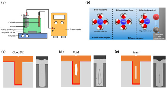
Figure 2. (a) Schematic illustration of an electroplating apparatus (reprinted with permission from [78]. Copyright 2016 The Multidisciplinary Digital Publishing Institute); (b) Schematic diagram of steps in electrodeposition as a function of the distance from the electrode (reprinted with permission from [79]. Copyright 2018 The Multidisciplinary Digital Publishing Institute); Schematic representation and SEM images of possible scenarios during electroplating such as (c) defect-free deposition and formation of the (d) void and (e) seam (reprinted with permission from [50]. Copyright 2017 Springer Nature).
There are four main reasons that electroplating is suitable when filling a nanoporous polymer template with heterogeneous materials. First, since solution-based electroplating is performed near room temperature, the thermal damage to nanostructure composed of polymer with a low glass transition temperature or melting point is negligible. Second, since electroplating exhibits a bottom-up growth behavior from the seed layer, templates with 3D nanoporous networks can be completely filled with heterogeneous materials to be electroplated. Third, since electroplating is a mature industrial technology, chemical recipes capable of electrodepositing various inorganic substances have been well developed and a batch process is available for mass production. Based on these good compatibilities between optical 3D lithography and electroplating, various 3D nanostructured inorganic materials have emerged. Figure 3 summarizes representative examples of the 3D nanostructured metals and semiconductors produced by template-assisted electroplating.
Various metals and alloys (Au, Cu, Ni, Ni-Sn, etc.) with 3D nanostructures have been successfully demonstrated. Gansel et al. reported the successful fabrication of a periodic array of tapered Au helix structures through the combination of DLW and electroplating (Figure 3a) [80]. Electroplating conditions with a constant electrical current of 0.6 μA were used to completely fill Au in a template with inverse helical structures. The polymer template was subsequently removed by air plasma treatment. Gu et al. created 3D meso-lattices made of Cu and Ni through electroplating using porous templates formed by DLW (Figure 3b) [81]. An indium tin oxide (ITO)-deposited glass cover slip was used as a conductive substrate for electroplating. A three-electrode electroplating system with a Pt counter electrode and an Ag/AgCl reference electrode was used to ensure the stability of the electroplating. To electroplate Cu and Ni into the templates, a Cu bath containing 125 g/L CuSO4·5H2O and 50 g/L H2SO4 and a Ni bath containing 240 g/L NiSO4·5H2O and 45 g/L NiCl2·6H2O and 40 g/L H3BO3·2H2O were used, respectively. The applied potential to the electrochemical cells was 2 V. After electroplating, the polymer template made of positive-tone photoresist (AZ4620, Microchem) was gently removed through a solution process with N-methylpyrrolidone (NMP), yielding metallic porous meso-lattices. Ning et al. reported the successful fabrication of 3D mesoporous Ni-Sn through the combination of MBIL and electroplating (Figure 3c) [53]. To achieve this, a mesoporous Ni scaffold was first prepared by 3D nanostructured template-assisted electroplating and subsequent template removal. Ni-Sn was then conformally grown on the mesoporous Ni scaffold through pulsed electroplating (0.2 s on and 10 s off) at –0.22 V by using an electrolyte composed of 0.06 M NiCl2, 0.2 M SnCl2, 1 M K4P2O7, 0.04 M potassium sodium tartrate, and 0.04 M glycine. The mesoporous MnO2 also can be produced in a similar way by using an electrolyte that contains 0.1 M Na2SO4, 0.1 M CH3COONa, and 0.1 M MnSO4. Kim et al. recently reported a large-scale 3D nanostructured Ni produced by template-assisted electroplating (Figure 3d) [82]. An inch-sized polymer template with 3D periodic nanostructure was first prepared by PnP. Then, Ni was bottom-up grown from the seed layer, which was pre-deposited on the substrate, through pulsed electroplating (5 s on and 5 s off) at 2 mA/cm2 to completely fill the 3D nanostructured template with Ni. The template was carefully removed by an ashier to yield porous Ni. In a similar way, Hyun et al. reported a 3D nanostructured Au with hierarchically arranged pores (Figure 3e) [83]. To achieve hierarchical porous structures, Au-Ag alloy was grown in the 3D nanostructured template by pulsed electrodeposition (5 s on and 5 s off) at an applied potential of -1.1 V. After template removal and selective etching of Ag through a dealloying procedure, a large-scale mesopore-in-macropore Au structure was produced.
This approach allows not only metals and alloys but also semiconductors to be 3D nanostructured materials. Xu et al. produced a 3D nanostructured titania (TiO2) by combining MBIL and electroplating (Figure 3f) [84]. To electroplate TiO2 on the template with a periodic 3D nanostructure defined by MBIL, electroplating was performed using a three-electrode system with a H2SO4-based aqueous solution of crystalline Ti powder with high purity (5N). The applied potential was controlled from 1.0 to 1.3 V and the constant current was 10 mA. Through optimization of the calcination process, the generation of thermal-induced defects in the 3D nanostructure during the template removal was significantly suppressed. In a similar way, Miyake et al. and Park et al. successfully developed 3D nanostructured Cu2O with face-centered cubic (FCC)-like and woodpile symmetries (Figure 3g) [22,23]. The polymer templates were patterned on ITO substrates via MBIL. A three-electrode electroplating system with an aqueous electrolyte containing 0.2 M cupric sulfate and 1.6 M lactic acid was used to deposit Cu2O on the templates. The pH of the solution was adjusted to ~9 by adding sodium hydroxide, and the temperature of the solution was kept constant at 65 °C during electroplating. To ensure complete filling of Cu2O in templates, a potentiostatic condition at -0.55 V was used. Through the template removal by reactive ion etching (RIE) under O2 and CF4 flows, highly symmetric inverse Cu2O structures were obtained.
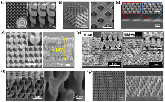
Figure 3. Various inorganic materials with 3D periodic nanostructures formed by template-assisted electroplating. (a) SEM images of Au helix structures formed by the combination of DLW and electroplating (Reprinted with permission from [80]. Copyright 2012 American Institute of Physics); (b) SEM images of a Cu meso-lattice formed by the combination of MBIL and electroplating (Reprinted with permission from [81]. Copyright 2015 Elsevier); (c) SEM images of mesoporous Ni-Sn electrodes formed by the combination of MBIL and electroplating (Reprinted with permission from [53]. Copyright 2015 The National Academy of Science); (d) SEM images of 3D nanostructured Ni formed by the combination of PnP and electroplating (Reprinted with permission from [82]. Copyright 2018 Elsevier); (e) SEM images of hierarchically porous Au nanostructures formed by PnP and electroplating (Reprinted with permission from [83]. Copyright 2020 The National Academy of Science); (f) SEM images of 3D nanostructured TiO2 formed by MBIL and electroplating (Reprinted with permission from [84]. Copyright 2005 The American Chemical Society); (g) SEM images of 3D nanostructured Cu2O formed by MBIL and electroplating (Reprinted with permission from [22]. Copyright 2009 WILEY-VCH).
2.3. Key Considerations for 3D Nanostructured Template-Assisted Electroplating
There are some special considerations needed when filling inorganic materials inside the polymer template with a 3D periodic nanostructure through electroplating. First, since the 3D nanostructured template to be formed on the substrate is a polymer-based insulator, optical 3D lithography introduced in the previous chapter must be preceded on a conductive substrate to enable electroplating. Second, plating conditions must be precisely controlled to ensure the complete filling of the material to be deposited in the 3D nanoporous network without voids or seams. Third, in order to extend the utility of the 3D nanostructured materials, it is desirable to be able to form a freestanding membrane separated from the substrate as needed.
Regarding the first issue, the most preferred approach is to perform optical 3D lithography (e.g., DLW, MBIL, or PnP) on a transparent and conductive substrate such as ITO or fluorine-doped tin oxide (FTO) glass coated with photoresist. At this time, it is very important to clean the substrate to improve the adhesion between the conductive substrate and the photoresist. Despite meticulous pretreatment of the substrate, 3D nanostructured films with high SVR formed by optical 3D lithography can be easily peeled off from ITO or FTO substrates. The reason is that the area of the surface structure formed by optical 3D lithography in contact with the substrate is small, so inherently poor adhesion between the substrate and the 3D nanostructured film cannot withstand the large swelling and shrinkage of the photoresist. The SU-8, which is a well-known epoxy-based negative-tone photoresist for the micro-electromechanical system (MEMS), generally suffers from 20~30% shrinkage during the development, rinsing, and drying steps. In particular, this problem often occurs as the result of MBIL and PnP. The resulting surface geometry of 3D periodic nanostructures generally consists of sharp and high-aspect-ratio nanopillars that form point contact rather than surface contact with the substrate, resulting in very poor adhesion with the substrate [85]. For this reason, in most cases, a hard-baked relatively thin (<2 μm) homogeneous photoresist film (e.g., SU-8) is pre-coated on the conductive seed layer-deposited substrate as an adhesive layer to maximize the bonding force between the substrate and the 3D nanostructured film with a thickness of 10 μm or more. The seed layer usually consists of highly conductive Cr/Au or Cu formed by sputtering or thermal evaporation. However, in template-assisted electroplating, the adhesive layer, which is a solid insulator, impedes the flow of current from the electrolyte to the seed layer (cathode) and does not allow electroplating. This is a significant practical concern that has not been dealt with so far. To solve this, a “window” process was developed and used (Figure 4). This process consists of three steps. 1) Through traditional photolithography, the adhesive layer is patterned to create an exposed part of the conductive seed layer. 2) Next, the entire substrate area is coated with photoresist and optical 3D lithography is performed. At this time, since the adhesive layer outside the “window” tightly holds the 3D nanostructured film well, delamination from the substrate does not occur. 3) Through electroplating, thin film growth occurs only in the area where the seed layer is exposed, filling the 3D nanostructured template with inorganic materials. This strategy makes it possible to perform the template-assisted electroplating with 3D nanostructured templates prepared by optical 3D lithography on an ad hoc basis [38,82,86]. However, the effect of light reflection from the metal seed layer on the formation of the 3D nanostructure has not yet been significantly considered. Ultimately, the development of an approach that fundamentally solves the problem of adhesion between the substrate and the 3D nanostructure is required. For example, a study to increase the contact area between the substrate and the 3D nanostructure through control of the surface roughness of the substrate, or to optimize the interfacial energy between the substrate and the 3D nanostructure through component control of the photoreactive polymer, may be considered as a follow-up study.
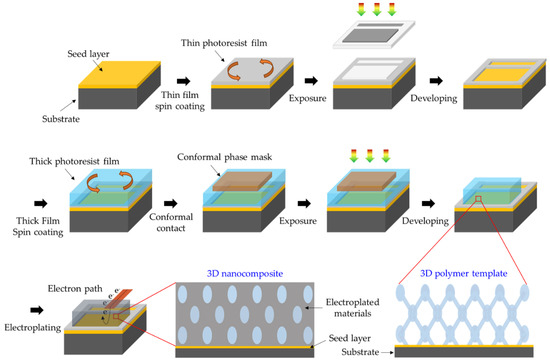
Figure 4. Schematic illustration of “window” process for electroplating inorganic materials into 3D porous templates.
Next, the complete filling of 3D nanostructured templates with inorganic materials without defects such as voids or seams is a very important issue as well in the electroplating step in relation to the quality and functionality of the resultant materials. When depositing a material by electroplating on a template with a nanoconfined structure rather than an open structure, this is more likely to result in non-uniform deposition that can cause voids or seams. One of the main reasons for non-uniform deposition is the lack of interaction between the hydrophilic components of the electrolyte solution and the hydrophobic polymer template. There are several ways to improve the uniformity of the filling while reducing defects, one of which is by adding surfactants to the solution (Figure 5a) [87–90]. For example, Shin et al. reported complete filling of Cu in a deep etched Si hole pattern by adding poly(ethylene glycol) (PEG), bis-(3-sodiumsulfopropyl disulfide) (SPS), and Janus Green B (JGB) [51]. PEG, SPS, and JGB act as a suppressor, an accelerator, and a leveler, respectively, during electroplating. PEG and JGB contributed to reducing the plating rate at the edges and surfaces of the hole pattern, while SPS contributed to increasing the plating rate inside the hole. Through the optimization of the concentration of each surfactant, void-free dense filling was achieved by compensating for the plating rate that varies locally across the hole pattern.
The current density is also an important variable that must be optimized for the defect-free filling of inorganics in the nanostructured templates. Essentially, as the current density increases, the plating rate or productivity increases. However, if the current density is too high, dendritic or tree-like structure growth is preferred, resulting in imperfect filling of the nanostructured templates. In addition, the current density tends to be maximized at the interface between the conductive part (seed layer) and the insulating part, so a thicker layer is generally formed at the edge of the substrate. This phenomenon is called as the edge effect. In the case of 3D nanostructured templates, this non-uniformity of the current density becomes more problematic since localized electrical interfaces are distributed over the entire area of the substrate and are continuously generated in volume as plating proceeds. To ensure the complete filling of the electroplated materials in the nanostructured templates, it is desirable to lower the current density to an optimum level for precisely controlling the plating rate. Such a strategy can be easily found in the case of the 3D packaging process, in which a metal should be completely filled in through silicon vias (TSVs) through electroplating for electrical interconnection [50]. When the high current density is applied, the outside of the hole is easily blocked with an electroplated film before even filling the inside of the hole. This is a highly fatal defect in the electrical interconnection that reduces the reliability of the device. On the other hand, if the current density is too low, the plating rate or productivity significantly decreases. The impurity level of the electroplated film may increase as well. Therefore, the current density should be maintained at an optimal level to ensure super-conformal deposition, which is closely related to the defect density of the nanostructured templates (Figure 5b).
The waveform of the current applied to the electrochemical cell is also an important variable in determining the quality of the filling in template-assisted electroplating. When a continuous current is applied, a negatively charged layer gradually covers the cathode surface during electroplating. This unwanted layer prevents further ions from reaching the cathode surface and causes non-uniform ion distribution. Pulse electroplating, in which the current is turned on and off periodically, can solve this problem by temporarily discharging the negatively charged inhibition layer (Figure 5c). More specifically, the non-uniform distribution of current density that occurs during electroplating can be compensated for by the redistribution of ions during the off state of repetitive pulsed cycles, which leads to homogeneous electroplating. Sometimes, pulse-reverse electroplating is used to improve the quality of the filling in the nanostructured template [91]. In this case, the stripping time with reverse current is introduced into the electroplating cycle. This allows the ion concentration to be replenished by convective diffusion toward the cathode surface and selectively dissolves protruding electroplated regions in the nanoconfined structure, resulting in much more homogeneous filling in the template. In addition, the use of additives resulting in complex process control can be neglected in pulse-reverse electroplating [91–93].
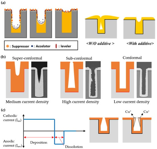
Figure 5. Schematic illustration of electroplating results corresponding to its parameters: (a) Additive (reprinted with permission from [51]. Copyright 2018 The Multidisciplinary Digital Publishing Institute); (b) Current density (reprinted with permission from [50]. Copyright 2017 Springer Nature); (c) Current waveform.
Lastly, most of the proposed functional materials with 3D periodic nanostructures, which have been manufactured by template-assisted electroplating, have served as a coating layer on the substrate. In order to maximize the utility of such a useful structure, it can be peeled off from the substrate and utilized as a freestanding and monolithic membrane as necessary. However, it is not easy to separate a highly porous thin film (depending on the photoresist thickness and generally less than tens of micrometers) from the substrate and handle it without destruction. Recently, Hong et al. reported a method of fabricating a 3D nanostructured composite membrane made of Bi-Sb-Te and epoxy by combining dry and wet etching processes (Figure 6) [38]. To briefly describe the process, first, a 3D nanostructured polymer template was formed on an SOI wafer with a thin Au seed layer through PnP, and Bi-SbTe, which is a useful thermoelectric material at room temperature, was electroplated into the template. The membranization process consists of two sequential steps. 1) The SiO2 layer is wet-etched by hydrogen fluoride (HF) solution to float the membrane; 2) the thin Au seed layer at the bottom of the membrane is carefully dry-etched by ion milling. In the process of selectively removing the sacrificial layer, it is very important to select the appropriate etching solution and precisely control the ion milling conditions to reduce damage to the electroplated material. The 3D nanostructured freestanding membrane implemented through this approach can be used in various ways such as flexible electronic devices. In the future, there is a need to develop a variety of membrane manufacturing methods optimized according to target applications.
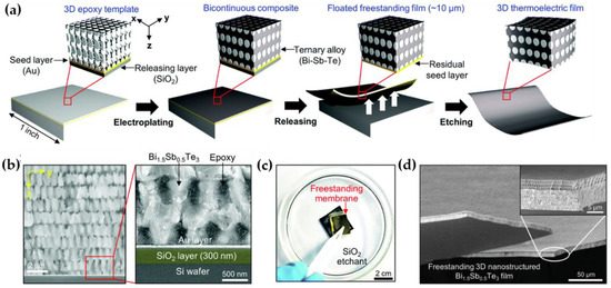
Figure 6. Fabrication process of a freestanding membrane: (a) Schematic illustration of fabricating a freestanding membrane; (b) SEM image of cross-sectional view of 3D nanostructured Bi-Sb-Te showing SiO2 layer as a sacrificial layer; (c) Digital image of a delaminated 3D sample from the Si substrate after wet etching process and (d) SEM image of a freestanding 3D nanostructured Bi-Sb-Te after dry etching process (reprinted with permission from [38]. Copyright 2017 The Royal Society of Chemistry).
References
- Velev, D.; Jede, T.A.; Lobo, R.F.; Lenhoff, A.M. Porous silica via colloidal crystallization. Nature 1997, 389, 447–448, doi:10.1038/38921.
- Shen, ; Zhang, L.; Chen, X.; Liu, L.; Zhang, D.; Han, Y.; Chen, J.; Long, J.; Luque, R.; Li, Y.; et al. Ordered macro-microporous metal-organic framework single crystals. Science 2018, 359, 206–210, doi:10.1126/science.aao3403.
- Dinsmore, D.; Hsu, M.F.; Nikolaides, M.G.; Marquez, M.; Bausch, A.R.; Weitz, D.A. Colloidosomes: Selectively Permeable Capsules Composed of Colloidal Particles. Science 2002, 298, 1006–1009, doi:10.1126/science.1074868.
- Vlasov, A.; Bo, X.-Z.; Sturm, J.C.; Norris, D.J. On-chip natural assembly of silicon photonic bandgap crystals. Nature 2001, 414, 289–293, doi:10.1038/35104529.
- Jiang, ; Cizeron, J.; Bertone, J.F.; Colvin, V.L. Preparation of Macroporous Metal Films from Colloidal Crystals. J. Am. Chem. Soc. 1999, 121, 7957–7958, doi:10.1021/ja991321h.
- Arpin, A.; Losego, M.D.; Cloud, A.N.; Ning, H.; Mallek, J.; Sergeant, N.P.; Zhu, L.; Yu, Z.; Kalanyan, B.; Parsons, G.N.; et al. Three-dimensional self-assembled photonic crystals with high temperature stability for thermal emission modification. Nat. Commun. 2013, 4, 2630, doi:10.1038/ncomms3630.
- Chan, Z.-H.; Hoffman, J.; Lee, V.Y.; Iatrou, H.; Avgeropoulos, A.; Hadjichristidis, N.; Miller, R.D.; Thomas, E.L. Ordered Bicontinuous Nanoporous and Nanorelief Ceramic Films from Self Assembling Polymer Precursors. Science 1999, 286, 1716–1719, doi:10.1126/science.286.5445.1716.
- Dolan, A.; Wilts, B.D.; Vignolini, S.; Baumberg, J.J.; Steiner, U.; Wilkinson, T.D. Optical Properties of Gyroid Structured Materials: From Photonic Crystals to Metamaterials. Adv. Opt. Mater. 2015, 3, 12–32, doi:10.1002/adom.201400333.
- Gratson, M.; Xu, M.; Lewis, J.A. Direct writing of three-dimensional webs. Nature 2004, 428, 386–386, doi:10.1038/428386a.
- Zaumseil, ; Meitl, M.A.; Hsu, J.W.P.; Acharya, B.R.; Baldwin, K.W.; Loo, Y.-L.; Rogers, J.A. Three-Dimensional and Multilayer Nanostructures Formed by Nanotransfer Printing. Nano Lett. 2003, 3, 1223–1227, doi:10.1021/nl0344007.
- Jeong, W.; Yang, S.R.; Hur, Y.H.; Kim, S.W.; Baek, K.M.; Yim, S.; Jang, H.-I.; Park, J.H.; Lee, S.Y.; Park, C.-O.; et al. High-resolution nanotransfer printing applicable to diverse surfaces via interface-targeted adhesion switching. Nat. Commun. 2014, 5, 5387, doi:10.1038/ncomms6387.
- Gansel, K.; Thiel, M.; Rill, M.S.; Decker, M.; Bade, K.; Saile, V.; Freymann, G.v.; Linden, S.; Wegener, M. Gold Helix Photonic Metamaterial as Broadband Circular Polarizer. Science 2009, 325, 1513–1515.
- Kawata, ; Sun, H.-B.; Tanaka, T.; Takada, K. Finer features for functional microdevices. Nature 2001, 412, 697–698.
- Peng, ; Zhang, R.; Chen, V.H.; Khabiboulline, E.T.; Braun, P.; Atwater, H.A. Three-dimensional single gyroid photonic crystals with a mid-infrared bandgap. ACS Photonics 2016, 3, 1131–1137.
- Radke, ; Gissibl, T.; Klotzbücher, T.; Braun, P.V.; Giessen, H. Three‐dimensional bichiral plasmonic crystals fabricated by direct laser writing and electroless silver plating. Adv. Mater. 2011, 23, 3018–3021.
- Deubel, ; von Freymann, G.; Wegener, M.; Pereira, S.; Busch, K.; Soukoulis, C.M. Direct laser writing of three-dimensional photonic-crystal templates for telecommunications. Nat. Mater. 2004, 3, 444–447.
- Rill, S.; Plet, C.; Thiel, M.; Staude, I.; Freymann, G.V.; Linden, S.; Wegener, M. Photonic metamaterials by direct laser writing and silver chemical vapour deposition. Nat. Mater. 2008, 7, 543–546.
- Bückmann, ; Stenger, N.; Kadic, M.; Kaschke, J.; Frölich, A.; Kennerknecht, T.; Eberl, C.; Thiel, M.; Wegener, M. Tailored 3D Mechanical Metamaterials Made by Dip‐in Direct‐Laser‐Writing Optical Lithography. Adv. Mater. 2012, 24, 2710–2714.
- Seet, K.; Mizeikis, V.; Matsuo, S.; Juodkazis, S.; Misawa, H. Three‐Dimensional Spiral‐Architecture Photonic Crystals Obtained By Direct Laser Writing. Adv. Mater. 2005, 17, 541–545.
- Wong, ; Deubel, M.; Pérez‐Willard, F.; John, S.; Ozin, G.A.; Wegener, M.; Freymann, G.v. Direct Laser Writing of Three‐Dimensional Photonic Crystals with a Complete Photonic Bandgap in Chalcogenide Glasses. Adv. Mater. 2006, 18, 265–269.
- Greiner, M.; Jäckel, M.; Scheiwe, A.C.; Stamow, D.R.; Autenrieth, T.J.; Lahann, J.; Franz, C.M.; Bastmeyer, M. Multifunctional polymer scaffolds with adjustable pore size and chemoattractant gradients for studying cell matrix invasion. Biomaterials 2014, 35, 611–619.
- Miyake, ; Chen, Y.C.; Braun, P.V.; Wiltzius, P. Fabrication of Three‐Dimensional Photonic Crystals Using Multibeam Interference Lithography and Electrodeposition. Adv. Mater. 2009, 21, 3012–3015.
- Park, G.; Miyake, M.; Yang, S.M.; Braun, P.V. Cu2O inverse Woodpile Photonic Crystals by Prism Holographic Lithography and Electrodeposition. Adv. Mater. 2011, 23, 2749–2752.
- Xia, ; Ku, Z.; Lee, S.C.; Brueck, S.R.J. Nanostructures and Functional Materials Fabricated by Interferometric Lithography. Adv. Mater. 2011, 23, 147–179.
- Moon, H.; Ford, J.; Yang, S. Fabricating three‐dimensional polymeric photonic structures by multi‐beam interference lithography. Polym. Adv. Technol. 2006, 17, 83–93.
- Yang, ; Megens, M.; Aizenberg, J.; Wiltzius, P.; Chaikin, P.M.; Russel, W.B. Creating Periodic Three-Dimensional Structures by Multibeam Interference of Visible Laser. Chem. Mater. 2002, 14, 2831–2833.
- Kang, -Y.; Lee, W.; Kim, D.; Moon, J.H. Three-Dimensional Polymeric Mechanical Metamaterials Fabricated by Multibeam Interference Lithography with the Assistance of Plasma Etching. Langmuir 2016, 32, 8436–8441.
- Hyun, K.; Park, J.; Kim, E.; Lauhon, L.J.; Jeon, S. Rational Control of Diffraction and Interference from Conformal Phase Gratings: Toward High‐Resolution 3D Nanopatterning. Adv. Opt. Mater. 2014, 2, 1213–1220.
- Park, ; Kim, K.I.; Kim, K.; Kim, D.C.; Cho, D.; Lee, J.H.; Jeon, S. Rapid, High‐Resolution 3D Interference Printing of Multilevel Ultralong Nanochannel Arrays for High‐Throughput Nanofluidic Transport. Adv. Mater. 2015, 27, 8000–8006.
- Park, ; Seo, J.; Jung, H.K.; Hyun, G.; Park, S.Y.; Jeon, S. Direct Optical Fabrication of Fluorescent, Multilevel 3D Nanostructures for Highly Efficient Chemosensing Platforms. Adv. Funct. Mater. 2016, 26, 7170–7177, doi:10.1002/adfm.201602601.
- Park, ; Wang, S.; Li, M.; Ahn, C.; Hyun, J.K.; Kim, D.S.; Kim, D.K.; Rogers, J.A.; Huang, Y.; Jeon, S. Three-dimensional nanonetworks for giant stretchability in dielectrics and conductors. Nat. Commun. 2012, 3, 916.
- Park, ; Yoon, S.; Kang, K.; Jeon, S. Antireflection behavior of multidimensional nanostructures patterned using a conformable elastomeric phase mask in a single exposure step. Small 2010, 6, 1981–1985.
- Nam, H.; Park, J.; Jeon, S. Rapid and Large‐Scale Fabrication of Full Color Woodpile Photonic Crystals via Interference from a Conformal Multilevel Phase Mask. Adv. Funct. Mater. 2019, 29, 1904971.
- Jeon, ; Park, J.-U.; Cirelli, R.; Yang, S.; Heitzman, C.E.; Braun, P.V.; Kenis, P.J.A.; Rogers, J.A. Fabricating complex three-dimensional nanostructures with high-resolution conformable phase masks. Proc. Natl. Acad. Sci. USA 2004, 101, 12428, doi:10.1073/pnas.0403048101.
- Park, ; Park, J.H.; Kim, E.; Ahn, C.W.; Jang, H.I.; Rogers, J.A.; Jeon, S. Conformable Solid-Index Phase Masks Composed of High-Aspect-Ratio Micropillar Arrays and Their Application to 3D Nanopatterning. Adv. Mater. 2011, 23, 860–864, doi:10.1002/adma.201003885.
- Park, ; Tahk, D.; Ahn, C.; Im, S.G.; Choi, S.-J.; Suh, K.-Y.; Jeon, S. Conformal phase masks made of polyurethane acrylate with optimized elastic modulus for 3D nanopatterning. J. Mater. Chem. C 2014, 2, 2316–2322, doi:10.1039/C3TC32194K.
- Cho, ; Ahn, C.; Park, J.; Jeon, S. 3D nanostructured N-doped TiO2 photocatalysts with enhanced visible absorption. Nanoscale 2018, 10, 9747–9751, doi:10.1039/C8NR02330A.
- Hong, ; Park, J.; Jeon, S.G.; Kim, K.; Park, S.H.; Shin, H.S.; Kim, B.; Jeon, S.; Song, J.Y. Monolithic Bi1.5Sb0.5Te3 ternary alloys with a periodic 3D nanostructure for enhancing thermoelectric performance. J. Mater. Chem. C 2017, 5, 8974–8980, doi:10.1039/C7TC02717F.
- George, C.; Nelson, E.C.; Rogers, J.A.; Braun, P.V. Direct Fabrication of 3D Periodic Inorganic Microstructures using Conformal Phase Masks. Angew. Chem. Int. Ed. 2009, 48, 144–148, doi:10.1002/anie.200804171.
- Chang, H.; Tian, L.; Hesse, W.R.; Gao, H.; Choi, H.J.; Kim, J.G.; Siddiqui, M.; Barbastathis, G. From Two-Dimensional Colloidal Self-Assembly to Three-Dimensional Nanolithography. Nano Lett. 2011, 11, 2533–2537, doi:10.1021/nl2011824.
- Jeon, Y.; Jeon, H.C.; Lee, S.Y.; Shim, T.S.; Kwon, J.-D.; Park, S.-G.; Yang, S.-M. 3D Hierarchical Architectures Prepared by Single Exposure Through a Highly Durable Colloidal Phase Mask. Adv. Mater. 2014, 26, 1422–1426, doi:10.1002/adma.201304317.
- Zhang, ; Yu, X.; Braun, P.V. Three-dimensional bicontinuous ultrafast-charge and -discharge bulk battery electrodes. Nat. Nanotechnol. 2011, 6, 277–281, doi:10.1038/nnano.2011.38.
- Long, W.; Dunn, B.; Rolison, D.R.; White, H.S. Three-Dimensional Battery Architectures. Chem. Rev. 2004, 104, 4463–4492, doi:10.1021/cr020740l.
- Novak, G.; Kim, K.; Jeon, S. 2D and 3D nanostructuring strategies for thermoelectric materials. Nanoscale 2019, 11, 19684–19699, doi:10.1039/C9NR07406F.
- Ahn, ; Kim, S.-M.; Jung, J.-W.; Park, J.; Kim, T.; Lee, S.E.; Jang, D.; Hong, J.-W.; Han, S.M.; Jeon, S. Multifunctional Polymer Nanocomposites Reinforced by 3D Continuous Ceramic Nanofillers. ACS Nano 2018, 12, 9126–9133, doi:10.1021/acsnano.8b03264.
- Cho, ; Shim, Y.-S.; Jung, J.-W.; Nam, S.-H.; Min, S.; Lee, S.-E.; Ham, Y.; Lee, K.; Park, J.; Shin, J.; et al. High-Contrast Optical Modulation from Strain-Induced Nanogaps at 3D Heterogeneous Interfaces. Adv. Sci. 2020, 7, 1903708, doi:10.1002/advs.201903708.
- Abbott, P.; Frisch, G.; Ryder, K.S. Electroplating using Ionic Liquids. Annu. Rev. Mater. Res. 2013, 43, 335–358.
- Moon, H.; Yang, S. Chemical Aspects of Three-Dimensional Photonic Crystals. Chem. Rev. 2010, 110, 547–574.
- Kuk, K.; Ham, Y.; Gopinath, K.; Boonmongkolras, P.; Lee, Y.; Lee, Y.W.; Kondaveeti, S.; Ahn, C.; Shin, B.; Lee, J.K.; et al. Continuous 3D Titanium Nitride Nanoshell Structure for Solar‐Driven Unbiased Biocatalytic CO2 Reduction. Adv. Energy Mater. 2019, 9, 1900029.
- Wang, ; Zhao, Z.; Nie, N.; Wang, F.; Zhu, W. Dynamic through-silicon-via filling process using copper electrochemical deposition at different current densities. Sci. Rep. 2017, 7, 46639.
- Shin, -H.; Kim, T.-Y.; Park, J.-H.; Suh, S.-J. Optimization of Additive and Current Conditions for Void-Free Filled Through-Silicon Via. Appl. Sci. 2018, 8, 2135.
- Shi, ; Wang, X.; Xu, C.; Yuan, J.; Fang, J.; Liu, S. Simulation and fabrication of two Cu TSV electroplating methods for wafer-level 3D integrated circuits packaging. Sens. Actuators A Phys. 2013, 203, 52–61.
- Ning, H.; Pikul, J.H.; Zhang, R.; Li, X.; Xu, S.; Wang, J.; Rogers, J.A.; King, W.P.; Braun, P.V. Holographic patterning of high-performance on-chip 3D lithium-ion microbatteries. Natl. Acad. Sci. USA 2015, 112, 6573-6578.
- Ahn, ; Park, J.; Cho, D.; Hyun, G.; Ham, Y.; Kim, K.; Nam, S.-H.; Bae, G.; Lee, K.; Shim, Y.-S.; et al. High-performance functional nanocomposites using 3D ordered and continuous nanostructures generated from proximity-field nanopatterning. Funct. Compos. Struct. 2019, 1, 032002, doi:10.1088/2631-6331/ab3692.
- Campbell, ; Sharp, D.N.; Harrison, M.T.; Denning, R.G.; Turberfield, A.J. Fabrication of photonic crystals for the visible spectrum by holographic lithography. Nature 2000, 404, 53, doi:10.1038/35003523.
- Kondo, ; Juodkazis, S.; Mizeikis, V.; Misawa, H.; Matsuo, S. Holographic lithography of periodic two-and three-dimensional microstructures in photoresist SU-8. Opt. Express 2006, 14, 7943–7953, doi:10.1364/OE.14.007943.
- Jeon, ; Kim, D.-H.; Park, S.-G. Holographic Fabrication of 3D Nanostructures. Adv. Mater. Interfaces 2018, 5, 1800330, doi:doi:10.1002/admi.201800330.
- Ullal, K.; Maldovan, M.; Thomas, E.L.; Chen, G.; Han, Y.-J.; Yang, S. Photonic crystals through holographic lithography: Simple cubic, diamond-like, and gyroid-like structures. Appl. Phys. Lett. 2004, 84, 5434–5436, doi:10.1063/1.1765734.
- Lee, -K.; Park, H.S.; Yi, G.-R.; Moon, J.H.; Yang, S.-M. Holographic Fabrication of Microstructures with Internal Nanopatterns Using Microprism Arrays. Angew. Chem. Int. Ed. 2009, 48, 7000–7005, doi:10.1002/anie.200901166.
- Shir, J.; Jeon, S.; Liao, H.; Highland, M.; Cahill, D.G.; Su, M.F.; El-Kady, I.F.; Christodoulou, C.G.; Bogart, G.R.; Hamza, A.V.; et al. Three-Dimensional Nanofabrication with Elastomeric Phase Masks. J. Phys. Chem. B 2007, 111, 12945–12958, doi:10.1021/jp074093j.
- Jeon, ; Malyarchuk, V.; Rogers, J.A.; Wiederrecht, G.P. Fabricating three dimensional nanostructures using two photon lithography in a single exposure step. Opt. Express 2006, 14, 2300–2308, doi:10.1364/OE.14.002300.
- Truong, T.; Lin, R.; Jeon, S.; Lee, H.H.; Maria, J.; Gaur, A.; Hua, F.; Meinel, I.; Rogers, J.A. Soft Lithography Using Acryloxy Perfluoropolyether Composite Stamps. Langmuir 2007, 23, 2898–2905, doi:10.1021/la062981k.
- Kwon, W.; Park, J.; Kim, T.; Kang, S.H.; Kim, H.; Shin, J.; Jeon, S.; Hong, S.W. Flexible Near-Field Nanopatterning with Ultrathin, Conformal Phase Masks on Nonplanar Substrates for Biomimetic Hierarchical Photonic Structures. ACS Nano 2016, 10, 4609–4617, doi:10.1021/acsnano.6b00816.
- Maria, ; Malyarchuk, V.; White, J.; Rogers, J.A. Experimental and computational studies of phase shift lithography with binary elastomeric masks. J. Vac. Sci. Technol. B Microelectron. Nanometer Struct. Process. Meas. Phenom. 2006, 24, 828–835, doi:10.1116/1.2184321.
- Sun, -B.; Nakamura, A.; Kaneko, K.; Shoji, S.; Kawata, S. Direct laser writing defects in holographic lithography-created photonic lattices. Opt. Lett. 2005, 30, 881–883, doi:10.1364/OL.30.000881.
- Braun, V.; Rinne, S.A.; García-Santamaría, F. Introducing Defects in 3D Photonic Crystals: State of the Art. Adv. Mater. 2006, 18, 2665–2678, doi:10.1002/adma.200600769.
- Singer, P.; Kooi, S.E.; Thomas, E.L. Focused laser spike (FLaSk) annealing of photoactivated chemically amplified resists for rapid hierarchical patterning. Nanoscale 2011, 3, 2730–2738, doi:10.1039/C1NR10050E.
- Wegener, 3-D Photonic Metamaterials Made by Direct Laser Writing. In Proceedings of Advanced Photonics & Renewable Energy, Karlsruhe, Germany, 21 June 2010; p. JMA1.
- Selimis, ; Mironov, V.; Farsari, M. Direct laser writing: Principles and materials for scaffold 3D printing. Microelectron. Eng. 2015, 132, 83–89, doi:10.1016/j.mee.2014.10.001.
- Sun, -B.; Kawata, S. Two-Photon Laser Precision Microfabrication and Its Applications to Micro-Nano Devices and Systems. J. Lightwave Technol. 2003, 21, 624.
- Jeon, ; Menard, E.; Park, J.-U.; Maria, J.; Meitl, M.; Zaumseil, J.; Rogers, J.A. Three-Dimensional Nanofabrication with Rubber Stamps and Conformable Photomasks. Adv. Mater. 2004, 16, 1369–1373, doi:10.1002/adma.200400593.
- Lee, -H.; Koh, C.Y.; Singer, J.P.; Jeon, S.-J.; Maldovan, M.; Stein, O.; Thomas, E.L. 25th Anniversary Article: Ordered Polymer Structures for the Engineering of Photons and Phonons. Adv. Mater. 2014, 26, 532–569, doi:10.1002/adma.201303456.
- Zhang, -L.; Chen, Q.-D.; Xia, H.; Sun, H.-B. Designable 3D nanofabrication by femtosecond laser direct writing. Nano Today 2010, 5, 435–448, doi:10.1016/j.nantod.2010.08.007.
- Sekkat, ; Kawata, S. Laser nanofabrication in photoresists and azopolymers. Laser Photonics Rev. 2014, 8, 1–26, doi:10.1002/lpor.201200081.
- Yarnitzky, ; Friedman, Y. Dynamic compensation of the over all and uncompensated cell resistance in a two-or three-electrode system. Steady state techniques. Anal. Chem. 1975, 47, 876–880.
- Prida, M.; Vega, V.; García, J.; Iglesias, L.; Hernando, B.; Minguez-Bacho, I. 1-Electrochemical methods for template-assisted synthesis of nanostructured materials. In Magnetic Nano- and Microwires; Vázquez, M., Ed.; Woodhead Publishing: Cambridge, UK, 2015; pp. 3–39, doi:10.1016/B978-0-08-100164-6.00001-1.
- Bera, ; Kuiry, S.C.; Seal, S. Synthesis of nanostructured materials using template-assisted electrodeposition. JOM 2004, 56, 49–53, doi:10.1007/s11837-004-0273-5.
- Tam, ; Palumbo, G.; Erb, U. Recent Advances in Superhydrophobic Electrodeposits. Materials 2016, 9, 151.
- Giurlani, ; Zangari, G.; Gambinossi, F.; Passaponti, M.; Salvietti, E.; Di Benedetto, F.; Caporali, S.; Innocenti, M. Electroplating for Decorative Applications: Recent Trends in Research and Development. Coatings 2018, 8, 260.
- Gansel, K.; Latzel, M.; Frölich, A.; Kaschke, J.; Thiel, M.; Wegener, M. Tapered gold-helix metamaterials as improved circular polarizers. Appl. Phys. Lett. 2012, 100, 101109.
- Wendy Gu, ; Greer, J.R. Ultra-strong architected Cu meso-lattices. Extrem. Mech. Lett. 2015, 2, 7–14, doi:10.1016/j.eml.2015.01.006.
- Kim, ; Ahn, C.; Cho, Y.; Hyun, G.; Jeon, S.; Park, J.H. Suppressing buoyant force: New avenue for long-term durability of oxygen evolution catalysts. Nano Energy 2018, 54, 184–191.
- Hyun, ; Song, J.T.; Ahn, C.; Ham, Y.; Cho, D.; Oh, J.; Jeon, S. Hierarchically porous Au nanostructures with interconnected channels for efficient mass transport in electrocatalytic CO2 reduction. Proc. Natl. Acad. Sci. USA 2020, 117, 5680–5685.
- Xu, ; Zhu, X.; Dan, Y.; Moon, J.H.; Chen, V.W.; Johnson, A.T.; Perry, J.W.; Yang, S. Electrodeposition of three-dimensional titania photonic crystals from holographically patterned microporous polymer templates. Chem. Mater. 2008, 20, 1816–1823.
- Ramanan, Fabrication of Novel Three-Dimensional Photonic Crystals Using Multi-Beam Interference Lithography; University of Illinois at Urbana-Champaign: Champaign, IL, USA, 2009.
- Kim, ; Tiwari, A.P.; Hyun, G.; Novak, T.G.; Jeon, S. Improving electrochemical active area of MoS2 via attached on 3D-ordered structures for hydrogen evolution reaction. Int. J. Hydrogen Energy 2019, 44, 28143–28150.
- Tang, ; Zhang, S.; Qiang, Y.; Chen, S.; Luo, L.; Gao, J.; Feng, L.; Qin, Z. 4, 6-Dimethyl-2-mercaptopyrimidine as a potential leveler for microvia filling with electroplating copper. RSC Adv. 2017, 7, 40342–40353.
- Xiao, ; Li, N.; Cui, G.; Tian, D.; Yu, S.; Li, Q.; Wu, G. Triblock Copolymers as Suppressors for Microvia Filling via Copper Electroplating. J. Electrochem. Soc. 2013, 160, D188–D195.
- Chrzanowska, ; Mroczka, R.; Florek, M. Effect of interaction between dodecyltrimethylammonium chloride (DTAC) and bis(3-sulphopropyl) disulphide (SPS) on the morphology of electrodeposited copper. Electrochim. Acta 2013, 106, 49–62.
- Ren, ; Lei, Z.; Wang, Z. Investigation of Nitrogen Heterocyclic Compounds as Levelers for Electroplating Cu Filling by Electrochemical Method and Quantum Chemical Calculation. J. Electrochem. Soc. 2015, 162, D509–D514.
- Zhu, S.; Toda, A.; Zhang, Y.; Itoh, T.; Maeda, R. Void-Free Copper Filling of Through Silicon Via by Periodic Pulse Reverse Electrodeposition. J. Electrochem. Soc. 2014, 161, D263–D268.
- Zhu, S.; Zhang, X.; Liu, C.Z.; Liu, H.Y. Effect of Reverse Pulse on Additives Adsorption and Copper Filling for Through Silicon Via. J. Electrochem. Soc. 2019, 166, D3006–D3012.
- Lin, ; Miao, J.; Dixit, P. Void formation over limiting current density and impurity analysis of TSV fabricated by constant-current pulse-reverse modulation. Microelectron. Reliab. 2013, 53, 1943–1953.
This entry is adapted from the peer-reviewed paper 10.3390/app10248780